CN1237654C - Two-port isolators and communicators - Google Patents
Two-port isolators and communicators Download PDFInfo
- Publication number
- CN1237654C CN1237654C CN 03145274 CN03145274A CN1237654C CN 1237654 C CN1237654 C CN 1237654C CN 03145274 CN03145274 CN 03145274 CN 03145274 A CN03145274 A CN 03145274A CN 1237654 C CN1237654 C CN 1237654C
- Authority
- CN
- China
- Prior art keywords
- electrode
- input
- central electrode
- port
- shape
- Prior art date
- Legal status (The legal status is an assumption and is not a legal conclusion. Google has not performed a legal analysis and makes no representation as to the accuracy of the status listed.)
- Expired - Fee Related
Links
- 229910000859 α-Fe Inorganic materials 0.000 claims abstract description 34
- 230000005291 magnetic effect Effects 0.000 claims description 12
- 238000012856 packing Methods 0.000 claims description 2
- 238000009413 insulation Methods 0.000 claims 2
- 230000001815 facial effect Effects 0.000 claims 1
- 238000002955 isolation Methods 0.000 abstract description 44
- 238000003780 insertion Methods 0.000 abstract description 43
- 230000037431 insertion Effects 0.000 abstract description 43
- 239000000758 substrate Substances 0.000 abstract description 42
- 238000004891 communication Methods 0.000 abstract description 12
- 239000003990 capacitor Substances 0.000 description 45
- 229910052751 metal Inorganic materials 0.000 description 25
- 239000002184 metal Substances 0.000 description 25
- 239000010410 layer Substances 0.000 description 7
- 230000003068 static effect Effects 0.000 description 6
- 239000000463 material Substances 0.000 description 5
- 238000010295 mobile communication Methods 0.000 description 5
- 238000007747 plating Methods 0.000 description 5
- 238000009966 trimming Methods 0.000 description 5
- 230000005540 biological transmission Effects 0.000 description 4
- 230000000052 comparative effect Effects 0.000 description 4
- 238000010586 diagram Methods 0.000 description 4
- 238000010304 firing Methods 0.000 description 4
- 238000000034 method Methods 0.000 description 4
- 230000035699 permeability Effects 0.000 description 4
- 229910052709 silver Inorganic materials 0.000 description 4
- 229910000679 solder Inorganic materials 0.000 description 4
- 230000000694 effects Effects 0.000 description 3
- 238000012545 processing Methods 0.000 description 3
- XEEYBQQBJWHFJM-UHFFFAOYSA-N Iron Chemical compound [Fe] XEEYBQQBJWHFJM-UHFFFAOYSA-N 0.000 description 2
- 230000000712 assembly Effects 0.000 description 2
- 238000000429 assembly Methods 0.000 description 2
- 229910052802 copper Inorganic materials 0.000 description 2
- 239000010949 copper Substances 0.000 description 2
- 238000011156 evaluation Methods 0.000 description 2
- 238000004519 manufacturing process Methods 0.000 description 2
- 239000000843 powder Substances 0.000 description 2
- 230000001629 suppression Effects 0.000 description 2
- 239000002344 surface layer Substances 0.000 description 2
- 229910018072 Al 2 O 3 Inorganic materials 0.000 description 1
- OKTJSMMVPCPJKN-UHFFFAOYSA-N Carbon Chemical compound [C] OKTJSMMVPCPJKN-UHFFFAOYSA-N 0.000 description 1
- RYGMFSIKBFXOCR-UHFFFAOYSA-N Copper Chemical compound [Cu] RYGMFSIKBFXOCR-UHFFFAOYSA-N 0.000 description 1
- KJTLSVCANCCWHF-UHFFFAOYSA-N Ruthenium Chemical compound [Ru] KJTLSVCANCCWHF-UHFFFAOYSA-N 0.000 description 1
- 229910004298 SiO 2 Inorganic materials 0.000 description 1
- BQCADISMDOOEFD-UHFFFAOYSA-N Silver Chemical compound [Ag] BQCADISMDOOEFD-UHFFFAOYSA-N 0.000 description 1
- 229910004116 SrO 2 Inorganic materials 0.000 description 1
- 239000000853 adhesive Substances 0.000 description 1
- 230000001070 adhesive effect Effects 0.000 description 1
- PNEYBMLMFCGWSK-UHFFFAOYSA-N aluminium oxide Inorganic materials [O-2].[O-2].[O-2].[Al+3].[Al+3] PNEYBMLMFCGWSK-UHFFFAOYSA-N 0.000 description 1
- 230000000903 blocking effect Effects 0.000 description 1
- ODINCKMPIJJUCX-UHFFFAOYSA-N calcium oxide Inorganic materials [Ca]=O ODINCKMPIJJUCX-UHFFFAOYSA-N 0.000 description 1
- 229910052799 carbon Inorganic materials 0.000 description 1
- 239000011195 cermet Substances 0.000 description 1
- 239000000470 constituent Substances 0.000 description 1
- 239000011889 copper foil Substances 0.000 description 1
- 238000005520 cutting process Methods 0.000 description 1
- 238000013461 design Methods 0.000 description 1
- 239000003989 dielectric material Substances 0.000 description 1
- 238000006073 displacement reaction Methods 0.000 description 1
- 239000003302 ferromagnetic material Substances 0.000 description 1
- 229910052737 gold Inorganic materials 0.000 description 1
- 229910052742 iron Inorganic materials 0.000 description 1
- 238000005304 joining Methods 0.000 description 1
- YEXPOXQUZXUXJW-UHFFFAOYSA-N lead(II) oxide Inorganic materials [Pb]=O YEXPOXQUZXUXJW-UHFFFAOYSA-N 0.000 description 1
- 229910052707 ruthenium Inorganic materials 0.000 description 1
- 239000004332 silver Substances 0.000 description 1
- 238000005476 soldering Methods 0.000 description 1
- 229910002076 stabilized zirconia Inorganic materials 0.000 description 1
- 238000004506 ultrasonic cleaning Methods 0.000 description 1
Images


Landscapes
- Non-Reversible Transmitting Devices (AREA)
Abstract
Description
技术领域technical field
本发明涉及两端口型隔离器,尤其涉及微波波段中使用的两端口型隔离器和通信装置。The invention relates to a two-port isolator, in particular to a two-port isolator and a communication device used in microwave bands.
背景技术Background technique
隔离器一般具有使信号仅在传送方向通过而反向传送受阻的功能,用于汽车电话、手机等移动通信设备的发送电路部。Isolators generally have the function of allowing signals to pass only in the transmission direction and blocking the reverse transmission, and are used in the transmission circuit of mobile communication devices such as car phones and mobile phones.
例如,作为这种隔离器,历来已公知两端口型隔离器(具有第一中心电极和第二中心电极的两个中心电极的隔离器)。该两端口型隔离器在将金属制下盒和金属制上盒接合而构成的金属盒内收装永久磁铁、铁氧体、配置在铁氧体主面的第一中心电极和第二中心电极、两个匹配电容以及电阻。通常第一中心电极和第二中心电极的形状相同,两个匹配电容的静电容也相同。For example, as such an isolator, a two-port type isolator (an isolator having two center electrodes of a first center electrode and a second center electrode) has been conventionally known. This two-port type isolator accommodates a permanent magnet, a ferrite, and a first center electrode and a second center electrode arranged on the main surface of the ferrite in a metal case formed by joining a metal lower case and a metal upper case. , two matching capacitors and resistors. Usually, the shape of the first center electrode and the second center electrode are the same, and the capacitances of the two matching capacitors are also the same.
配合通信系统决定移动通信设备所用两端口型隔离器要求的插入损耗特性和隔离特性。因此,对实际两端口型隔离器具有的插入损耗特性和隔离特性与通信系统的要求规格进行比较时,有时虽然隔离特性足够宽裕,满足要求规格,却插入损耗特性达不到要求规格。反之,插入损耗特性足够宽裕,满足要求规格,隔离特性却达不到要求规格。The insertion loss characteristics and isolation characteristics required for two-port isolators used in mobile communication equipment are determined in conjunction with the communication system. Therefore, when comparing the insertion loss characteristics and isolation characteristics of an actual two-port type isolator with the required specifications of a communication system, there may be cases where the insertion loss characteristics do not meet the required specifications although the isolation characteristics are sufficient to meet the required specifications. Conversely, the insertion loss characteristic is sufficient to meet the required specification, but the isolation characteristic cannot meet the required specification.
另一方面,移动通信设备中,为了抑制发送电路部耗电,增加连续通话时间,强烈希望即使让隔离特性有些劣化,也要降低插入损耗。然而,已有技术没有满足这种希望的手段,不能调整两端口型隔离器的插入损耗特性和隔离特性。On the other hand, in mobile communication equipment, in order to reduce the power consumption of the transmission circuit and increase the continuous call time, it is strongly desired to reduce the insertion loss even if the isolation characteristics are slightly deteriorated. However, the prior art has no means to satisfy this desire, and cannot adjust the insertion loss characteristics and isolation characteristics of the two-port type isolator.
因此,本发明的目的在于提供能调整插入损耗特性和隔离特性的两端口型隔离器和通信装置。Therefore, an object of the present invention is to provide a two-port type isolator and a communication device capable of adjusting insertion loss characteristics and isolation characteristics.
发明内容Contents of the invention
为了达到上述目的,本发明的两端口型隔离器,包括In order to achieve the above object, the two-port isolator of the present invention comprises
(a)永久磁铁、(a) Permanent magnets,
(b)由永久磁铁施加直流磁场的铁氧体、(b) Ferrite to which a DC magnetic field is applied by a permanent magnet,
(c)配置在铁氧体的主面或内部并且一端电连接第一输入输出端口而另一端电连接第二输入输出端口的第一中心电极、(c) a first central electrode arranged on the main surface or inside of the ferrite and one end electrically connected to the first input and output port and the other end electrically connected to the second input and output port,
(d)与第一中心电极在电绝缘的状态下交叉配置在铁氧体的主面或内部并且一端电连接第二输入输出端口而另一端电连接第三端口的第二中心电极、(d) a second central electrode that is electrically insulated from the first central electrode and is arranged on the main surface or inside of the ferrite and that has one end electrically connected to the second input-output port and the other end electrically connected to the third port,
(e)电连接在第一输入输出端口与第二输入输出端口之间的第一匹配电容、(e) a first matching capacitor electrically connected between the first input and output port and the second input and output port,
(f)电连接在第一输入输出端口与第二输入输出端口之间的电阻、和(f) a resistor electrically connected between the first input-output port and the second input-output port, and
(g)电连接在第二输入输出端口与第三端口之间的第二匹配电容,(g) a second matching capacitor electrically connected between the second input and output port and the third port,
(h)其中第三端口电接地,而且第一中心电极的电感L1与第二中心电极的电感L2不同。(h) The third port is electrically grounded, and the inductance L1 of the first center electrode is different from the inductance L2 of the second center electrode.
此外,本发明的两端口型隔离器,包括In addition, the two-port type isolator of the present invention includes
(i)永久磁铁、(i) permanent magnets,
(j)由永久磁铁施加直流磁场的铁氧体、(j) Ferrite to which a DC magnetic field is applied by a permanent magnet,
(k)配置在铁氧体的主面或内部并且一端电连接第一输入输出端口而另一端电连接第二输入输出端口的第一中心电极、(k) a first central electrode arranged on the main surface or inside of the ferrite and one end electrically connected to the first input and output port and the other end electrically connected to the second input and output port,
(l)与第一中心电极在电绝缘的状态下交叉配置在铁氧体的主面或内部并且一端电连接第二输入输出端口而另一端电连接第三端口的第二中心电极、(1) The first central electrode is electrically insulated from the second central electrode disposed on the main surface or inside of the ferrite and one end is electrically connected to the second input and output port and the other end is electrically connected to the third port,
(m)电连接在第一输入输出端口与第二输入输出端口之间的第一匹配电容、(m) a first matching capacitor electrically connected between the first input and output port and the second input and output port,
(n)电连接在第二输入输出端口与第三端口之间的第二匹配电容、和(n) a second matching capacitor electrically connected between the second input and output port and the third port, and
(o)电连接在第三端口与地之间的电阻,(o) a resistor electrically connected between the third port and ground,
(p)其中第一中心电极的电感L1与第二中心电极的电感L2不同。(p) wherein the inductance L1 of the first center electrode is different from the inductance L2 of the second center electrode.
为了使第一中心电极的电感L1与第二中心电极的电感L2不同,例如可使两者的电极宽度、电极厚度、电极长度、电极根数、电极间隔等不同。又,铁氧体俯视可为矩形或圆形。而且,配合第一和第二中心电极的电感L1、L2将第一和第二匹配电容的静电容C1、C2分别设定为最佳值。In order to make the inductance L1 of the first center electrode different from the inductance L2 of the second center electrode, for example, the electrode width, electrode thickness, electrode length, electrode number, electrode interval, etc. of the two may be different. Also, the ferrite can be rectangular or circular in plan view. Moreover, the electrostatic capacitances C1 and C2 of the first and second matching capacitors are respectively set to optimum values in conjunction with the inductances L1 and L2 of the first and second center electrodes.
根据以上结构,第一中心电极的电感L1小于第二中心电极的电感L2时(L1<L2时),随着L1与L2的差增大,隔离的带宽变窄,插入损耗的带宽变置。反之,第一中心电极的电感L1大于第二中心电极的电感L2时(L1>L2时),随着L1与L2的差增大,隔离的带宽变置,插入损耗的带宽变窄。According to the above structure, when the inductance L1 of the first center electrode is smaller than the inductance L2 of the second center electrode (when L1<L2), as the difference between L1 and L2 increases, the isolation bandwidth narrows and the insertion loss bandwidth changes. Conversely, when the inductance L1 of the first center electrode is greater than the inductance L2 of the second center electrode (L1>L2), as the difference between L1 and L2 increases, the isolation bandwidth changes and the insertion loss bandwidth narrows.
本发明的两端口型隔离器,具有包装永久磁铁、铁氧体、第一和第二中心电极的金属盒,金属盒具有上面部、底面部以及连接该上面部和底面部的一对相互对置的侧面部,第一中心电极和第二中心电极的任一个配置在对于侧面部大致垂直的方向,另一中心电极配置在对于侧面部大致平行的方向。The two-port isolator of the present invention has a metal case for packing permanent magnets, ferrite, and first and second center electrodes, and the metal case has an upper portion, a bottom portion, and a pair of opposite sides connecting the upper portion and the bottom portion. Either one of the first center electrode and the second center electrode is arranged in a direction substantially perpendicular to the side surface, and the other center electrode is arranged in a direction substantially parallel to the side surface.
根据以上的结构,配置成对金属盒中连接上面部和底面部的侧面部大致垂直的中心电极容易在上面部和底面部流过接地电流,配置成对所述侧面部大致平行的中心电极不容易在上面部和底面部流过接地电流。因此,即使第一中心电极和第二中心电极形状相同,也能使两者的电感L1和L2不同。According to the above structure, the center electrode arranged so as to be substantially perpendicular to the side surface connecting the upper part and the bottom part of the metal box is likely to have a ground current flow through the upper part and the bottom part, and the center electrode arranged so as to be substantially parallel to the side part is not. A ground current tends to flow through the upper surface and the bottom surface. Therefore, even if the first center electrode and the second center electrode have the same shape, the inductances L1 and L2 of the two can be made different.
而且,电连接第一输入输出端口的第一输入输出外部电极和电连接第二输入输出端口的第二输入输出外部电极可分别设置在两端口型隔离器的一对相互对置侧面的中央位置。由此,在手机等的印刷电路板上安装两端口型隔离器时只要使该隔离器旋转180度,就能安装在将输入信号线路和输出信号线路设定成左右相反的印刷电路板上。因而,不需要配合印刷电路板输入信号线路和输出信号线路的方向制作2种两端口型隔离器。Also, a first input-output external electrode electrically connected to the first input-output port and a second input-output external electrode electrically connected to the second input-output port may be respectively provided at a central position of a pair of side faces of the two-port type isolator. . As a result, when mounting a two-port isolator on a printed circuit board such as a mobile phone, the isolator can be mounted on a printed circuit board in which input signal lines and output signal lines are set to the left and right by rotating the isolator 180 degrees. Therefore, there is no need to make two types of two-port type isolators according to the direction of the input signal line and the output signal line of the printed circuit board.
又,本发明的通信装置具有上述两端口型隔离器,因而特性提高。Furthermore, since the communication device of the present invention includes the above-mentioned two-port isolator, its characteristics are improved.
附图说明Description of drawings
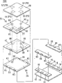
图1是示出本发明所涉及两端口型隔离器一实施形态的分解立体图。FIG. 1 is an exploded perspective view showing an embodiment of a two-port isolator according to the present invention.
图2是图1所示中心电极组装体的俯视图。FIG. 2 is a top view of the center electrode assembly shown in FIG. 1 .
图3是图1所示叠层基板的分解立体图。FIG. 3 is an exploded perspective view of the laminated substrate shown in FIG. 1 .
图4是图1所示两端口型隔离器的外观立体图。Fig. 4 is an external perspective view of the two-port isolator shown in Fig. 1 .
图5是图1所示两端口型隔离器的电等效电路图。FIG. 5 is an electrical equivalent circuit diagram of the two-port isolator shown in FIG. 1 .
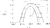
图6是示出隔离特性的曲线。Fig. 6 is a graph showing isolation characteristics.
图7是示出插入损耗特性的曲线。Fig. 7 is a graph showing insertion loss characteristics.
图8是示出输入反射损耗特性的曲线。FIG. 8 is a graph showing input return loss characteristics.
图9是示出输出反射损耗特性的曲线。FIG. 9 is a graph showing output reflection loss characteristics.
图10是示出C1/C2的比率与隔离度的关系的曲线。FIG. 10 is a graph showing the relationship between the ratio of C1/C2 and the degree of isolation.
图11是示出C1/C2的比率与插入损耗的关系的曲线。FIG. 11 is a graph showing the relationship between the ratio of C1/C2 and insertion loss.
图12是示出C1/C2的比率与输出反射损耗的关系的曲线。FIG. 12 is a graph showing the relationship between the ratio of C1/C2 and the output reflection loss.
图13是示出本发明所涉及两端口型隔离器另一实施形态的分解立体图。Fig. 13 is an exploded perspective view showing another embodiment of the two-port isolator according to the present invention.
图14是图13所示叠层基板的分解立体图。FIG. 14 is an exploded perspective view of the laminated substrate shown in FIG. 13 .
图15是示出本发明所涉及两端口型隔离器又一实施形态的分解立体图。Fig. 15 is an exploded perspective view showing still another embodiment of the two-port isolator according to the present invention.
图16是图15所示叠层基板的分解立体图。Fig. 16 is an exploded perspective view of the laminated substrate shown in Fig. 15 .
图17是图15所示两端口型隔离器的电等效电路图。FIG. 17 is an electrical equivalent circuit diagram of the two-port isolator shown in FIG. 15 .
图18是示出隔离特性的曲线。Fig. 18 is a graph showing isolation characteristics.
图19是示出插入损耗特性的曲线。Fig. 19 is a graph showing insertion loss characteristics.
图20是示出输入反射损耗特性的曲线。Fig. 20 is a graph showing input return loss characteristics.
图21是示出输出反射损耗特性的曲线。Fig. 21 is a graph showing output reflection loss characteristics.
图22是示出C1/C2的比率与隔离度的关系的曲线。FIG. 22 is a graph showing the relationship between the ratio of C1/C2 and the degree of isolation.
图23是示出C1/C2的比率与插入损耗的关系的曲线。FIG. 23 is a graph showing the relationship between the ratio of C1/C2 and insertion loss.
图24是示出C1/C2的比率与输入反射损耗的关系的曲线。FIG. 24 is a graph showing the relationship between the ratio of C1/C2 and the input return loss.
图25是本发明所涉及通信装置的电路框图。Fig. 25 is a circuit block diagram of a communication device according to the present invention.
图26是示出中心电极组装体变换例的仰视图。Fig. 26 is a bottom view showing a modified example of the center electrode assembly.
图27是示出中心电极组装体另一变换例的仰视图。Fig. 27 is a bottom view showing another modified example of the center electrode assembly.
图28是示出中心电极组装体又一变换例的俯视图。Fig. 28 is a plan view showing still another modified example of the center electrode assembly.
图29是示出中心电极组装体又一变换例的俯视图。Fig. 29 is a plan view showing still another modified example of the center electrode assembly.
图30是示出中心电极组装体又一变换例的俯视图。Fig. 30 is a plan view showing still another modified example of the center electrode assembly.
图31是示出中心电极组装体又一变换例的俯视图。Fig. 31 is a plan view showing still another modified example of the center electrode assembly.
附图中,1、1A、1B为集中常数型隔离器,4为金属制上盒,8为金属制下盒,9为永久磁铁,13、13A~13H为中心电极组装体,14为输入外部电极,15为输出外部电极,16为接地外部电极,20为铁氧体,21为第一中心电极,22为第二中心电极,21a、21b、22a、22b为端部,30、30A、30B为叠层基板,41~45为介电片,55、56、57为电容电极,58为接地电极,220为手机,25、26为匹配电容,27为电阻,P1为输入端口(第一输入输出端口),P2为输出端口(第二输入输出端口),P3为接地端口(第三端口)。In the accompanying drawings, 1, 1A, 1B are lumped constant type isolators, 4 is a metal upper case, 8 is a metal lower case, 9 is a permanent magnet, 13, 13A~13H are center electrode assemblies, and 14 is an input external Electrode, 15 is output external electrode, 16 is ground external electrode, 20 is ferrite, 21 is first center electrode, 22 is second center electrode, 21a, 21b, 22a, 22b are ends, 30, 30A, 30B 41 to 45 are dielectric sheets, 55, 56, and 57 are capacitor electrodes, 58 is a ground electrode, 220 is a mobile phone, 25 and 26 are matching capacitors, 27 is a resistor, and P1 is an input port (the first input output port), P2 is the output port (the second input and output port), and P3 is the ground port (the third port).
具体实施方式Detailed ways
下面,参照附图说明本发明所涉及两端口型隔离器和通信装置的实施形态。Embodiments of a two-port isolator and a communication device according to the present invention will be described below with reference to the drawings.
实施形态1(图1~图12)Embodiment 1 (Fig. 1 to Fig. 12)
图1示出本发明所涉及两端口型隔离器一实施形态的分解立体图。该两端口型隔离器1是集中常数型隔离器。如图1所示,两端口型隔离器1大致具有由金属上盒4和金属下盒8组成的金属盒、永久磁铁9、由铁氧体20和中心电极21与22组成的电极组装体13以及叠层基板30。FIG. 1 shows an exploded perspective view of an embodiment of a two-port isolator according to the present invention. This two-
金属上盒4大致为箱状,由上面部4a和4个侧面部4b组成。金属下盒8由底面部8a和左右的侧面部8b组成。金属上盒4和金属下盒8形成磁路,因而用例如软铁等强磁性体构成的材料形成,并且其表面镀Ag或Cu。The metal
中心电极组装体13在圆板状微波铁氧体20的上表面将2组第一和第二中心电极21、22配置成以绝缘层(未示出)为中介相互垂直交叉。在实施形态1中,按两行组成中心电极21、22。第一中心电极21和第二中心电极22各自的两个端部21a、21b、22a、22b在铁氧体20的下表面延伸,各端部21a~22b相互分离。In the
如图2所示,第一中心电极21的电极宽度W1与第二中心电极22的电极宽度不同。由此,使第一中心电极21的电感L1与第二中心电极22的电感L2不同。本实施形态1通过使电极宽度W1和W2不同,让电感L1和L2不同,但未必限于此,例如使第一中心电极21的电极厚度t1和第二中心电极22的电极厚度t2不同,使第一中心电极的电极长度11和第二中心电极长度12不同,使第一中心电极的电极间隔S1和第二中心电极22的电极间隔S2不同,或者上述各点的组合,也可让电感L1和L2不同。As shown in FIG. 2 , the electrode width W1 of the first
这里,中心电极21、22的电极宽度W1、W2越窄,电感L1、L2越大。电极厚度t1、t2越薄,电感L1、L2越大。电极长度11、12越长,电感L1、L2越大。电极间隔S1、S2越窄,电感L1、L2越大。Here, the narrower the electrode widths W1, W2 of the
中心电极21、22可用铜箔卷绕在铁氧体20上,也可用银糊印制到铁氧体20上或其内部而形成。或者,也可如特开平9-232818号公报记载的那样,用叠层基板形成。但是,印制的方法使中心电极21、22的位置精度高,因而与叠层基板30的连接稳定。尤其本案,在用微小的中心电极用连接电极51~54(后文说明)进行连接时,印制形成中心电极21、22的方法可靠性、操作性良好。The
如图3所示,叠层基板30由中心电极用连接电极51~54、在背面设置电容电极55和56与电阻27的介电片41、在背面设置电容电极57的介电片42、在背面设置接地电极58的介电片43、设置输入外部电极14和输出外部电极15和接地外部电极16的介电片45等构成。中心电极用连接电极51作为输入端口P1,中心电极用连接电极53、54作为输出端口P2,中心电极用连接电极52作为第三端口P3。As shown in FIG. 3 , the
此叠层基板30制作如下。即,用低温烧结介电材料制作介电片41~45,该介电材料包含Al2O3作为主成分,SiO2、SrO2、CaO、PbO、Na2O、K2O、MgO、BaO、CeO2、B2O3中的一种或多种作为副成分。This
制作抑制叠层基板30在基板平面方向(X-Y方向)烧固收缩的收缩抑制片46、47,使其在叠层基板30的烧固条件下(尤其在烧固温度1000℃以下)不烧固。该收缩抑制片46、47的材料是氧化铝粉末和稳定的氧化锆粉末的混合材料。片41~47的厚度为10μm~200μm左右。Make
在片41~43、46的背面利用图案印刷等方法形成电极51~58。作为电极51~58的材料,可用电阻率低且能与介电片41~45同时烧固的Ag、Cu、Ag-Pd等。电极51~58的厚度为2μm~20μm左右。电极51~58等的厚度通常设定为表皮厚度的2倍以上。
在介电片41的背面利用图案印刷等方法形成电阻27。作为电阻27的材料,使用金属陶瓷、碳、钌等。电阻27也可印刷在叠层基板30的上表面形成,还可用片状电阻形成。The
通过利用激光加工或冲压加工等预先在介电片41~45形成通路的用的孔后,在该孔填充导电糊,形成通路孔60、侧面通路孔65和外部电极14~16。Via holes 60 , side via
使电容电极57与电容电极45对置,将介电片42夹在其中间,以构成匹配电容25。进而,使电容电极57与电容电极56和接地电极58对置,将介电片42、43夹在其中间,以构成匹配电容26。这些匹配电容25、26和电阻27与电极51~54、外部电极14~16和通路孔60、65一起在叠层基板30的内部构成电路。The matching
将以上的介电片41~45叠层,进而从介电片41~45的叠层体上下两侧用收缩抑制片46、47夹入后,进行烧固。由此,得到烧结体后,利用超声波清洁法或湿式珩磨法去除未烧结的收缩抑制材料,就成为图1所示的叠层基板30。The above-mentioned dielectric sheets 41 to 45 are laminated, and the laminated body of the dielectric sheets 41 to 45 is sandwiched by the
叠层基板30的两端部分别设置输入外部电极14、输出外部电极所15和接地外部电极16。输入外部电极14电连接电容电极55,输出外部电极15电连接电容电极57。接地外部电极16电连接接地电极58。然后,将Ni镀层作为基底,进行镀Au。Ni镀层增强电极的Ag与Au镀层的粘接强度。Au镀层使软钎料的浸润性良好,同时导电率高,因而使隔离器1损耗小。The input
该叠层基板30通常按母板状态制成。该母板以规定的间距形成半切断的槽,沿该槽折断,就从母板得到所希望的尺寸的叠层基板30。或者,也可用切片机或激光切断母板,以切出所希望尺寸的叠层基片30。The
这样得到的叠层基片30内部具有匹配电容25、26和电阻27。按所需静电容值精度制作匹配电容25、26。然而,进行修整时,在对匹配电容25、26和中心电极21、22进行连接前进行。即,叠层基板30在单体的状态下,将内部(第二层)的电容电极55、56与表层的介电体一起修整(切边)。修整中采用切削机或YAG的基波、2次谐波、3次谐波激光。采用激光,则可锝速度快且精度高的加工。也可对母板状态的叠层基波30高效进行修整。The
这样,将叠层基板30接近上表面的电容电极55、56作为修整用电容电极,因而能使修整时去除的介电层的厚度最小。又由于成为修整障碍的电极减少(实施形态1时仅为连接电极51~54),可修整的电容电极区扩大,使静电容调整范围可加大。In this way, since the
叠层基板30还内置电阻37,并且与匹配电容25、26相同,电阻27也与表层介电体一起进行修整,因而能调整电阻值R。电阻27即使在~处宽度变细时,电阻值R也升高,因而切削到宽度方向的中部。The
以上的组成部件组装如下。即,如图1所示,在金属制上盒4的顶部用粘接剂固定永久磁铁9。用软钎料80将中心电极组装体13的中心电极21、23各自的端部21a~22b电连接到叠层基板30表面形成的中心电极用连接电极51~54,在叠层基板30上安装中心电极组装体13。对母板状态的叠层基板30也可高效进行中心电极21、22与中心电极用连接电极51~54的软钎焊。The above constituent parts are assembled as follows. That is, as shown in FIG. 1 , the
叠层基板30装在金属制下盒8的底面部8a上,用软钎料80将叠层基板30下表面配置的接地电极58连接并固定到底面部8a。由此,接地端口16便于电连接底面部8a。The
然后,金属制下盒8与金属制上盒4用软钎料等接合各自的侧面部8b与4b,以构成金属盒,并且也作为磁轭起作用。即,该金属盒形成包围永久磁铁9、中心电极组装体13和叠层基板30的磁路。永久磁铁9还对铁氧体20施加直流磁场。Then, the metal
这样,就得到图4所示的两端口型隔离器1。图5是隔离器1的电等效电路。第一中心电极21的一个端部21a通过输入端口(中心电极用连接电极51)电连接输入外部电极14。第一中心电极21的另一端部21b通过输出端口P2(中心电极用连接电极54)电连接输出外部电极15。第二中心电极22的一个端部22a通过输出端口P2(中心电极用连接电极53)电连接输出外部电极15。第二中心电极22的另一端部22b通过第三端口P3(中心电极用连接电极52)电连接到接地外部电极16。由匹配电容25和电阻27组成的并联RC电路电连接在输入端口In this way, the two-
P1与输出端口P2之间。匹配电容26连接在输出端口P2与第三端口P3之间。第三端口P电连接接地。Between P1 and output port P2. The matching
以上组成部分构成的两端口型隔离器1使第一中心电极21的电感L1与第二中心电极22的电感L2不同,并且L1<L2时,随着L1与L2的差变大,隔离的带宽变窄,插入损耗的带宽变宽。反之,L1>L2时,随着L1与L2的差变大,隔离的带宽变宽,插入损耗的带宽变窄。即,通过调整L1和L2的值,可根据通信系统的要求规格调整隔离的带宽和插入损耗的带宽。The two-
另一方面,随着使中心电极21、22的电感L1、L2相互不同,也需要使匹配电容25、26的静电容C1、C2不同(设定为最佳静电容C1、C2)。即,需要使L1和C1以及L2和C2的并联谐振电路统一为相同的谐振频率。因此,本发明用叠层基板30内配置的电极55~58形成匹配电容25、26。由此,借助使电极55~58的对置面积和间隔不同,能方便地使匹配电容25、26的静电容C1、C2不同。On the other hand, as the inductances L1 and L2 of the
图6、图7、图8和图9各曲线分别示出如表1一1所示那样对两端口型隔离器1中第一和第二中心电极21、22的电感L1、L2和匹配电容25、26的静电容C1、C2作种种改变时的隔离特性、插入损耗特性、输入反射损耗特性和输出反射损耗特性。The curves of Fig. 6, Fig. 7, Fig. 8 and Fig. 9 respectively show the inductance L1, L2 and matching capacitance of the first and second
这里,作为铁氧体20,采用直径2.0mm、厚度0.4mm的铁氧体。而且,取中心电极21、22的电极宽度W为0.2mm,电极间隔S为0.2mm,电极长度1为2mm,将自感设定为0.7nH。又取中心电极21、22的电极宽度W为0.5mm,电极间隔S为0.2mm,电极长度1为2mm,将自感设定为0.5nH。再取中心电极21、22的电极宽度W为0.1mm,电极间隔S为0.1mm,电极长度1为2mm,将自感设定为1.0nH。电阻27的电阻值R均为60Ω。表1-1中的电感是假设相对导磁率为1时的中心电极21、22的自感,实际上该值乘以铁氧体20等的有效导磁率所得的值才等于电感L1、L2。表1-2归纳893MHz~960MHz频带内最坏值。Here, as the
【表1】【Table 1】
(表1-1)
(表1-2)
从图6~图9和表1-2可知,如实施例1那样,使第一中心电极21的自感小于第二中心电极22的自感,虽然隔离度变差,但插入损耗和反射损耗改善。From Figures 6 to 9 and Tables 1-2, it can be seen that, as in Example 1, the self-inductance of the
反之,可知:如实施例2那样,使第一中心电极21的自感大于第二中心电极22的自感,虽然插入损耗和反射损耗变差,但隔离度提高。On the contrary, it can be seen that if the self-inductance of the
这样使两个中心电极21、22的自感为不同的值,能优化插入损耗和隔离度,可提供特性优良的隔离器1。In this way, the self-inductances of the two
移动通信设备用的的两端口型隔离器通常要求的插入损耗为1.2dB以下,隔离度为8.0dB以上,因此,通过对匹配电容25、26的静电容比率C1/C2作种种改变,研究出满足此条件的两端口型隔离器1。表2是其评价结果,图10、图11和图12的曲线分别示出隔离特性、插入损耗特性和输出反射损耗特性。The two-port type isolator used in mobile communication equipment usually requires an insertion loss of 1.2dB or less and an isolation of 8.0dB or more. Therefore, by making various changes to the electrostatic capacitance ratio C1/C2 of the matching
【表2】【Table 2】
(表2)
从表2和图10、图11可见,在希望插入损耗为1.2dB以下且隔离度为8.0dB以上的范围内隔离优良的两端口型隔离器1时,设计成C1/C2的值满足关系式0.5≤C1/C2≤0.9为佳。其原因在于C1/C2为0.9以下,则隔离度可改善0.5dB,而C1/C2小于0.5时,隔离度进一步改善,但插入损耗超过1.2dB,变坏到不能实用。It can be seen from Table 2 and Figures 10 and 11 that when a two-
在希望插入损耗为1.2dB以下且隔离度为8.0dB以上的范围内隔离优良的两端口型隔离器1时,设计成C1/C2的值满足关系式1.1≤C1/C2≤3.0为佳。其原因在于C1/C2为1.1以上,则插入损耗可改善0.05dB,而C1/C2~超过3.0时,插入损耗进一步改善,但隔离度超过8.0dB,变坏到不能实用。When a two-
在3端口型隔离器(具有第一~第三中心电极等3个中心电极的隔离器)的情况下,如特开2001-185914号公报、特开2001-203007号公报和特开2001-203508号公报所记载,已公知使中心电极电感不同的结构。然而,这些3端口型隔离器用电极宽度等调整结构上为非对称的部分。In the case of a 3-port type isolator (an isolator having three center electrodes such as the first to third center electrodes), such as JP-A-2001-185914, JP-A-2001-203007, and JP-A-2001-203508 As described in the Publication No. 1, a structure in which the inductance of the center electrodes is made different is known. However, in these 3-port type isolators, the structurally asymmetric part is adjusted by electrode width and the like.
与此相反,本发明积极地做成非对称结构,将隔离度和插入损耗设定为所希望的特性。而且,3端口型隔离器虽然使中心电极电感不同,但不能对隔离的带宽和插入损耗的带宽作折衷调整。只有中心电极21的两个端部21a、21b连接输入输出端口P1、P2的本发明两端口型隔离器才能得到这种作用的效果。On the contrary, the present invention positively makes an asymmetric structure, and sets isolation and insertion loss to desired characteristics. Furthermore, although the 3-port type isolator makes the inductance of the center electrodes different, it cannot make a trade-off adjustment between the isolation bandwidth and the insertion loss bandwidth. Only the two-port type isolator of the present invention in which the two
实施形态2(图13和图14)Embodiment 2 (Figure 13 and Figure 14)
图13所示的两端口型隔离器1A除中心电极组装体13A和叠层基板30A外,其余与所述实施形态1的两端口型隔离器1相同。A two-port isolator 1A shown in FIG. 13 is the same as the two-
中心电极组装体13A配置成使第一和第二中心电极21、22以绝缘层(未示出)为中介在铁氧体20的上表面相互交叉。第一和第二中心电极21、22的形状(电极宽度、电极厚度、电极长度、电极间隔等)相同。The
如图14所示,叠层基板30A的组成部分包含中心电极用连接电极51~54、背面设置电容电极55和电阻27的介电片41、背面设置电容电极57的介电片42、背面设置接地电极58的介电片43、设置输入外部电极14、输出外部电极15和接地外部电极16的介电片45等。利用与所述实施形态1的叠层基板30相同的方法制作该叠层基板30A。As shown in FIG. 14 , the components of the
电容电极57与电容电极55对置,将介电片42夹在其中间,以构成匹配电容25。电容电极57又与接地电极58对置,将介电片43夹在其中间,以构成匹配电容26。The
中心电极用连接电极51~54配置在叠层基板30A的4个边各自的中央部附近。输入外部电极14和输出外部电极15配置在叠层基板30A上2条对置边的中央部。中心电极用连接电极51成为输入端口P1,中心电极用连接电极53、54成为输出端口P2,中心电极用连接电极52成为第三端口P3。The
以上结构组成的中心电极组装体13A在叠层基板30A上安装,2组中心电极21、22的某一个,使其对与金属制上盒4接合的金属制下盒8的侧面部8b垂直。配置在对侧面部8b垂直的方向的中心电极22容易使接地电流流到金属盒的上面部4a和底面部8a,配置在对侧面部8b平行的方向的中心电极21使接地电流难以流到金属盒的上面部4a和底面部8a。因此,即使中心电极21和22的形状相同,其电感L1和L2也不同。
于是,两端口型隔离器1A得到与所述实施形态1的隔离器1相同的作用效果。接地电流由输入输出外部电极14、15连接的电源装置(未示出)产生,并且流过隔离器1A内各种路径。例如,接地电流按输入外部电极14-中心电极21-中心电极22-接地外部电极16的路径顺序流通,或按输入外部电极14-中心电极21-匹配电容C2(位移电流)-接地外部电极16和路径顺序流通。Accordingly, the two-port isolator 1A obtains the same effect as the
本实施形态2将输入外部电极14和输出外部电极15设置在隔离器1A的一对相互对置侧面的中央位置。由此,在手机等的印刷电路板上安装隔离器1A时,将隔离器1A旋转180度,就可装在输入信号线路与输出信号线路配置成左右相反的印刷电路板上。因此,不需要配合印刷电路板输入信号线路和输出信号线路的方向制作2种隔离器1A,能使隔离器1A成本降低。In the second embodiment, the input
尤其该两端口型隔离器1A在将端口P1作为输入端口时和将端口P2作为输入端口时,反射损耗频率特性大为不同,不需要制作不仅磁场方向相反(永久磁铁9的NS方向相反)而且内部结构改变的2中隔离器1A,因而降低成本的效果大。In particular, in this two-port isolator 1A, when the port P1 is used as the input port and the port P2 is used as the input port, the return loss frequency characteristics are greatly different, and it is not necessary to manufacture not only the direction of the magnetic field (the NS direction of the
实施形态3(图15~图24)Embodiment 3 (Fig. 15 to Fig. 24)
图15所示的两端口型隔离器1B除中心电极组装体13B和叠层基板30B外,其余与所述实施形态1的两端口型隔离器1相同。The two-
中心电极组装体13B配置成使第一和第二中心电极21、22以绝缘层(未示出)为中介在铁氧体20的上表面相互交叉。第一和第二中心电极21、22的形状(电极宽度、电极厚度、电极长度、电极间隔等)相同。The
如图16所示,叠层基板30B的组成部分包含中心电极用连接电极51~53、背面设置电容电极55、59和电阻27的介电片41、背面设置电容电极57的介电片42、背面设置接地电极58的介电片43、设置输入外部电极14、输出外部电极15和接地外部电极16的介电片45等。As shown in FIG. 16 , the components of the
电容电极57与电容电极55、59对置,将介电片42夹在其中间,以分别构成匹配电容25、26。The
中心电极用连接电极53为长带状,其一个端部53b侧通过介电片41、42上设置的通路孔60电连接电容电极57。由此,第一中心电极21的实际电极长度,其尺寸为第中心电极21本身的长度加上从中心电极用连接电极53的端部53a(焊接中心电极21侧的端部)到连接通路孔60的位置的长度。改变通路孔60的位置,就能调整第一中心电极21和第二中心电极22的实际电极长度。The connecting
结果,能使第一中心电极21的实际电感L1与第二中心电极22的实际电感L2不同,可根据通信系统的要求规格调整两端口型隔离器1B的隔离带宽和插入损耗带宽。这时,中心电极用连接电极53与通路孔60连接的位置成为输出端口P2的位置。而且,中心电极用连接电极51为输入端口P1,中心电极用连接电极52为第三端口P3。As a result, the actual inductance L1 of the
还能减少叠层基板30B上形成的通路孔60的数量和连接部位,可降低制造成本。而且,利用减少通路孔60的数量可扩大一张片子内能形成的电极面积,能加大匹配电容25、26的静电容。It is also possible to reduce the number of via
图27是上述那样取得的两端口型隔离器1B的电等效电路。在输入端口P1与输出端口P2之间连接由第一中心电极21和第一匹配电容25组成的LC并联谐振电路。在输出端口P2与第三端口P3之间连接第二中心电极22和第二匹配电容26组成的LC并联谐振电路。还在第三端口P3与接地外部电极16之间连接终端电阻27。FIG. 27 is an electrical equivalent circuit of the two-
图18、图19、图20和图21的曲线分别示出如表3-1那样对两端口型隔离器1B的第一和第二中心电极21、22的实际电感L1、L2和匹配电容25、26的静电容C1、C2作种种改变时的隔离特性、插入损耗特性、输入反射特性和输出反射损耗特性。电阻27的电阻值R均为60Ω。表3-1中的电感是假设相对导磁率为1时的中心电极21、22的实际自感,实际上该电感乘以铁氧体20的有效导磁率所得的值才等于电感L1、L2。表3-2归纳893MHz~960MHz频带内最坏值。The curves of Fig. 18, Fig. 19, Fig. 20 and Fig. 21 respectively show the actual inductance L1, L2 and matching
【表3】【table 3】
(表3-1)
(表3-2)
从图18~图21和表3-2可知,如实施例3那样,使第一中心电极21的自感小于第二中心电极22的自感,虽然隔离度变差,但插入损耗和反射损耗改善。From Figures 18 to 21 and Table 3-2, it can be seen that, as in Example 3, the self-inductance of the
反之,可知:如实施例4那样,使第一中心电极21的自感大于第二中心电极22的自感,虽然插入损耗和反射损耗变差,但隔离度提高。On the contrary, it can be seen that, as in Example 4, if the self-inductance of the
这样使两个中心电极21、22的自感为不同的值,能优化插入损耗和隔离度,可提供特性优良的隔离器1B。In this way, the self-inductances of the two
移动通信设备用的的两端口型隔离器通常要求的插入损耗为1.2dB以下,隔离度为8.0dB以上,因此,通过对匹配电容25、26的静电容比率C1/C2作种种改变,研究出满足此条件的两端口型隔离器1B。表4是其评价结果,图22、图23和图24的曲线分别示出隔离特性、插入损耗特性和输入反射损耗特性。The two-port type isolator used in mobile communication equipment usually requires an insertion loss of 1.2dB or less and an isolation of 8.0dB or more. Therefore, by making various changes to the electrostatic capacitance ratio C1/C2 of the matching
【表4】【Table 4】
(表4)
从表4和图22、图23可见,设计成C1/C2的值满足关系式1.1≤C1/C2≤2.0,能得到插入损耗为1.2dB以下且隔离度为8.0dB以上的两端口型隔离器1B。It can be seen from Table 4 and Figure 22 and Figure 23 that the value of C1/C2 is designed to satisfy the relationship 1.1≤C1/C2≤2.0, and a two-port isolator with an insertion loss of less than 1.2dB and an isolation of more than 8.0dB can be obtained 1B.
实施形态4(图25)Embodiment 4 (Figure 25)
实施形态4将便携电话作为例子说明本发明的通信装置。
图25是手机220中RF(射频)部分的电路框图。图25中,222是天线元件,223是双工器,231是发送侧隔离器,232是发送侧放大器,233是发送侧级间带通滤波器,234是发送侧混频器,235是接收侧放大器,236是接收侧级间带通滤波器,237是接收侧混频器,238是压控振荡器,239是本机带通滤波器。FIG. 25 is a circuit block diagram of the RF (radio frequency) part of the mobile phone 220. As shown in FIG. In Fig. 25, 222 is an antenna element, 223 is a duplexer, 231 is a transmitting side isolator, 232 is a transmitting side amplifier, 233 is a transmitting side interstage bandpass filter, 234 is a transmitting side mixer, 235 is a receiving side Side amplifier, 236 is the receiving side interstage bandpass filter, 237 is the receiving side mixer, 238 is the voltage controlled oscillator, 239 is the local bandpass filter.
这里,作为发送侧隔离器231,可用所述实施形态1~3的两端口型隔离器1、1A、1B。安装这些隔离器,能实现电特性改善且可靠性高的便携电话。Here, as the transmission-side isolator 231, the two-
其他实施形态Other implementation forms
本发明不限于上述实施形态,在其要旨的范围内能作种种变换。例如,使永久磁铁9的N极和S极颠倒,则能调换输入端口P1和输出端口P2。The present invention is not limited to the above-described embodiments, and various changes can be made within the scope of the gist. For example, by reversing the N pole and S pole of the
中心电极组装体也能作种种变换。例如,图26所示中心电极组装体13C那样,可将铁氧体20背面设置的中心电极21的长度分别在纵向延长13,使中心电极21和22的长度不同。这时,将叠层基板30的中心电极用连接电极51、54的位置移动到内侧。还可如图27所示中心电极组装体13D那样,将铁氧体20背面配置的中心电极21和22的端部21b和22a加以电连接。这时,能省略叠层基板30的中心电极用连接电极53和54中的某一个,可减少通路孔数量。The center electrode assembly can also be changed in various ways. For example, as in the center electrode assembly 13C shown in FIG. 26 , the lengths of the
或者,如图28~图30分别示出的中心电极组装体13E、13F、13G那样,中心电极21和22可不相互平行,也可弯曲,还可电极根数不同。而且,如图31所示中心电极组装体13H那样,可用矩形的铁氧体20。这时,第一中心电极21配置成与铁氧体20的短边平行,第二中心电极22配置成与铁氧体20的长边平行。Alternatively, as in the
以上说明中可知,根据本发明,通过使第一中心电极和第二中心电极的电感为不同的值,能优化插入损耗和隔离度,可提供特性优良的两端口型隔离器。因而,能得到高性能、高可靠性且体积小的两端口型隔离器和通信装置。As can be seen from the above description, according to the present invention, by setting the inductances of the first center electrode and the second center electrode to different values, insertion loss and isolation can be optimized, and a two-port isolator having excellent characteristics can be provided. Therefore, a high-performance, high-reliability, and small-sized two-port type isolator and communication device can be obtained.
Claims (15)
Applications Claiming Priority (2)
| Application Number | Priority Date | Filing Date | Title |
|---|---|---|---|
| JP2002188516 | 2002-06-27 | ||
| JP2002188516 | 2002-06-27 |
Publications (2)
| Publication Number | Publication Date |
|---|---|
| CN1471193A CN1471193A (en) | 2004-01-28 |
| CN1237654C true CN1237654C (en) | 2006-01-18 |
Family
ID=34179451
Family Applications (1)
| Application Number | Title | Priority Date | Filing Date |
|---|---|---|---|
| CN 03145274 Expired - Fee Related CN1237654C (en) | 2002-06-27 | 2003-06-27 | Two-port isolators and communicators |
Country Status (1)
| Country | Link |
|---|---|
| CN (1) | CN1237654C (en) |
Families Citing this family (7)
| Publication number | Priority date | Publication date | Assignee | Title |
|---|---|---|---|---|
| CN100492758C (en) * | 2004-07-30 | 2009-05-27 | 株式会社村田制作所 | Dual-port isolator and communication device |
| WO2006013865A1 (en) * | 2004-08-03 | 2006-02-09 | Hitachi Metals, Ltd. | Non-reciprocal circuit element |
| WO2007013253A1 (en) * | 2005-07-28 | 2007-02-01 | Murata Manufacturing Co., Ltd. | Irreversible circuit element, composite electronic parts, and communication device |
| WO2007013252A1 (en) * | 2005-07-28 | 2007-02-01 | Murata Manufacturing Co., Ltd. | Irreversible circuit element, composite electronic parts, and communication device |
| JP4858542B2 (en) * | 2007-01-18 | 2012-01-18 | 株式会社村田製作所 | Non-reciprocal circuit element |
| JP5170139B2 (en) * | 2010-03-23 | 2013-03-27 | 株式会社村田製作所 | Circuit module |
| JP7170685B2 (en) * | 2020-03-19 | 2022-11-14 | 株式会社東芝 | isolator |
-
2003
- 2003-06-27 CN CN 03145274 patent/CN1237654C/en not_active Expired - Fee Related
Also Published As
| Publication number | Publication date |
|---|---|
| CN1471193A (en) | 2004-01-28 |
Similar Documents
| Publication | Publication Date | Title |
|---|---|---|
| CN1254161C (en) | Circuit board and circuit device and manufacturing method thereof | |
| CN1248355C (en) | Low-pass filter | |
| EP1094538A2 (en) | Multilayered ceramic RF device | |
| CN1402426A (en) | Multi-layer LC composite element and mfg. method thereof | |
| CN1625845A (en) | Switching circuits and composite high-frequency devices | |
| CN105122443A (en) | High-frequency components and high-frequency modules equipped with them | |
| US6765460B2 (en) | Dielectric laminated device including a buried electric conductive member to form a strip line and its method of manufacture | |
| CN1460397A (en) | High-frequency module | |
| CN1148091C (en) | Non-reciprocal circuit devices and communication devices incorporating such devices | |
| CN101080843A (en) | Non-reciprocal circuit element, method for manufacturing the same, and communication device | |
| CN1472841A (en) | Two port isolator and communication device | |
| CN1237654C (en) | Two-port isolators and communicators | |
| CN1295885C (en) | High frequency switch, radio communication apparatus, and high frequency switching method | |
| CN1324760C (en) | Three-port irreversible circuit element, composite electronic component, and communication device | |
| CN1149705C (en) | non-reciprocal circuit device | |
| CN1330375A (en) | Wave filter | |
| JP3835437B2 (en) | 2-port isolator and communication device | |
| CN1233064C (en) | Three-port nonreciprocal circuit device and communication apparatus | |
| US6900704B2 (en) | Two-port isolator and communication device | |
| CN1950972A (en) | Two-port nonreciprocal circuit device and communication device | |
| CN1257574C (en) | Irreversible Circuit Module | |
| JP3858852B2 (en) | 2-port isolator and communication device | |
| CN1591966A (en) | Two-port isolator, characteristic adjusting method therefor, and communication apparatus | |
| CN1728447A (en) | High frequency circuit module having non-reciprocal circuit element | |
| CN1270404C (en) | Non-reversable circuit element and its producing method |
Legal Events
| Date | Code | Title | Description |
|---|---|---|---|
| C06 | Publication | ||
| PB01 | Publication | ||
| C10 | Entry into substantive examination | ||
| SE01 | Entry into force of request for substantive examination | ||
| C14 | Grant of patent or utility model | ||
| GR01 | Patent grant | ||
| CF01 | Termination of patent right due to non-payment of annual fee |
Granted publication date: 20060118 |
|
| CF01 | Termination of patent right due to non-payment of annual fee |