CN1248552C - Printed circuit board with improved pad structure - Google Patents
Printed circuit board with improved pad structure Download PDFInfo
- Publication number
- CN1248552C CN1248552C CNB021222908A CN02122290A CN1248552C CN 1248552 C CN1248552 C CN 1248552C CN B021222908 A CNB021222908 A CN B021222908A CN 02122290 A CN02122290 A CN 02122290A CN 1248552 C CN1248552 C CN 1248552C
- Authority
- CN
- China
- Prior art keywords
- pads
- printed circuit
- circuit board
- edge
- rectangular
- Prior art date
- Legal status (The legal status is an assumption and is not a legal conclusion. Google has not performed a legal analysis and makes no representation as to the accuracy of the status listed.)
- Expired - Fee Related
Links
Images


Classifications
-
- H—ELECTRICITY
- H05—ELECTRIC TECHNIQUES NOT OTHERWISE PROVIDED FOR
- H05K—PRINTED CIRCUITS; CASINGS OR CONSTRUCTIONAL DETAILS OF ELECTRIC APPARATUS; MANUFACTURE OF ASSEMBLAGES OF ELECTRICAL COMPONENTS
- H05K3/00—Apparatus or processes for manufacturing printed circuits
- H05K3/30—Assembling printed circuits with electric components, e.g. with resistors
- H05K3/32—Assembling printed circuits with electric components, e.g. with resistors electrically connecting electric components or wires to printed circuits
-
- H—ELECTRICITY
- H05—ELECTRIC TECHNIQUES NOT OTHERWISE PROVIDED FOR
- H05K—PRINTED CIRCUITS; CASINGS OR CONSTRUCTIONAL DETAILS OF ELECTRIC APPARATUS; MANUFACTURE OF ASSEMBLAGES OF ELECTRICAL COMPONENTS
- H05K3/00—Apparatus or processes for manufacturing printed circuits
- H05K3/30—Assembling printed circuits with electric components, e.g. with resistors
- H05K3/32—Assembling printed circuits with electric components, e.g. with resistors electrically connecting electric components or wires to printed circuits
- H05K3/34—Assembling printed circuits with electric components, e.g. with resistors electrically connecting electric components or wires to printed circuits by soldering
- H05K3/341—Surface mounted components
- H05K3/3431—Leadless components
- H05K3/3436—Leadless components having an array of bottom contacts, e.g. pad grid array or ball grid array components
-
- H—ELECTRICITY
- H05—ELECTRIC TECHNIQUES NOT OTHERWISE PROVIDED FOR
- H05K—PRINTED CIRCUITS; CASINGS OR CONSTRUCTIONAL DETAILS OF ELECTRIC APPARATUS; MANUFACTURE OF ASSEMBLAGES OF ELECTRICAL COMPONENTS
- H05K1/00—Printed circuits
- H05K1/02—Details
- H05K1/11—Printed elements for providing electric connections to or between printed circuits
- H05K1/111—Pads for surface mounting, e.g. lay-out
-
- H—ELECTRICITY
- H10—SEMICONDUCTOR DEVICES; ELECTRIC SOLID-STATE DEVICES NOT OTHERWISE PROVIDED FOR
- H10W—GENERIC PACKAGES, INTERCONNECTIONS, CONNECTORS OR OTHER CONSTRUCTIONAL DETAILS OF DEVICES COVERED BY CLASS H10
- H10W70/00—Package substrates; Interposers; Redistribution layers [RDL]
- H10W70/60—Insulating or insulated package substrates; Interposers; Redistribution layers
- H10W70/62—Insulating or insulated package substrates; Interposers; Redistribution layers characterised by their interconnections
- H10W70/65—Shapes or dispositions of interconnections
-
- H—ELECTRICITY
- H05—ELECTRIC TECHNIQUES NOT OTHERWISE PROVIDED FOR
- H05K—PRINTED CIRCUITS; CASINGS OR CONSTRUCTIONAL DETAILS OF ELECTRIC APPARATUS; MANUFACTURE OF ASSEMBLAGES OF ELECTRICAL COMPONENTS
- H05K2201/00—Indexing scheme relating to printed circuits covered by H05K1/00
- H05K2201/09—Shape and layout
- H05K2201/09209—Shape and layout details of conductors
- H05K2201/09218—Conductive traces
- H05K2201/09227—Layout details of a plurality of traces, e.g. escape layout for Ball Grid Array [BGA] mounting
-
- H—ELECTRICITY
- H05—ELECTRIC TECHNIQUES NOT OTHERWISE PROVIDED FOR
- H05K—PRINTED CIRCUITS; CASINGS OR CONSTRUCTIONAL DETAILS OF ELECTRIC APPARATUS; MANUFACTURE OF ASSEMBLAGES OF ELECTRICAL COMPONENTS
- H05K2201/00—Indexing scheme relating to printed circuits covered by H05K1/00
- H05K2201/09—Shape and layout
- H05K2201/09209—Shape and layout details of conductors
- H05K2201/09372—Pads and lands
- H05K2201/094—Array of pads or lands differing from one another, e.g. in size, pitch or thickness; Using different connections on the pads
-
- H—ELECTRICITY
- H05—ELECTRIC TECHNIQUES NOT OTHERWISE PROVIDED FOR
- H05K—PRINTED CIRCUITS; CASINGS OR CONSTRUCTIONAL DETAILS OF ELECTRIC APPARATUS; MANUFACTURE OF ASSEMBLAGES OF ELECTRICAL COMPONENTS
- H05K2201/00—Indexing scheme relating to printed circuits covered by H05K1/00
- H05K2201/09—Shape and layout
- H05K2201/09209—Shape and layout details of conductors
- H05K2201/09372—Pads and lands
- H05K2201/09409—Multiple rows of pads, lands, terminals or dummy patterns; Multiple rows of mounted components
-
- H—ELECTRICITY
- H05—ELECTRIC TECHNIQUES NOT OTHERWISE PROVIDED FOR
- H05K—PRINTED CIRCUITS; CASINGS OR CONSTRUCTIONAL DETAILS OF ELECTRIC APPARATUS; MANUFACTURE OF ASSEMBLAGES OF ELECTRICAL COMPONENTS
- H05K2201/00—Indexing scheme relating to printed circuits covered by H05K1/00
- H05K2201/09—Shape and layout
- H05K2201/09209—Shape and layout details of conductors
- H05K2201/09372—Pads and lands
- H05K2201/09418—Special orientation of pads, lands or terminals of component, e.g. radial or polygonal orientation
-
- H—ELECTRICITY
- H05—ELECTRIC TECHNIQUES NOT OTHERWISE PROVIDED FOR
- H05K—PRINTED CIRCUITS; CASINGS OR CONSTRUCTIONAL DETAILS OF ELECTRIC APPARATUS; MANUFACTURE OF ASSEMBLAGES OF ELECTRICAL COMPONENTS
- H05K2201/00—Indexing scheme relating to printed circuits covered by H05K1/00
- H05K2201/10—Details of components or other objects attached to or integrated in a printed circuit board
- H05K2201/10613—Details of electrical connections of non-printed components, e.g. special leads
- H05K2201/10621—Components characterised by their electrical contacts
- H05K2201/10734—Ball grid array [BGA]; Bump grid array
-
- H—ELECTRICITY
- H10—SEMICONDUCTOR DEVICES; ELECTRIC SOLID-STATE DEVICES NOT OTHERWISE PROVIDED FOR
- H10W—GENERIC PACKAGES, INTERCONNECTIONS, CONNECTORS OR OTHER CONSTRUCTIONAL DETAILS OF DEVICES COVERED BY CLASS H10
- H10W72/00—Interconnections or connectors in packages
- H10W72/071—Connecting or disconnecting
- H10W72/075—Connecting or disconnecting of bond wires
-
- H—ELECTRICITY
- H10—SEMICONDUCTOR DEVICES; ELECTRIC SOLID-STATE DEVICES NOT OTHERWISE PROVIDED FOR
- H10W—GENERIC PACKAGES, INTERCONNECTIONS, CONNECTORS OR OTHER CONSTRUCTIONAL DETAILS OF DEVICES COVERED BY CLASS H10
- H10W72/00—Interconnections or connectors in packages
- H10W72/50—Bond wires
- H10W72/551—Materials of bond wires
-
- H—ELECTRICITY
- H10—SEMICONDUCTOR DEVICES; ELECTRIC SOLID-STATE DEVICES NOT OTHERWISE PROVIDED FOR
- H10W—GENERIC PACKAGES, INTERCONNECTIONS, CONNECTORS OR OTHER CONSTRUCTIONAL DETAILS OF DEVICES COVERED BY CLASS H10
- H10W72/00—Interconnections or connectors in packages
- H10W72/851—Dispositions of multiple connectors or interconnections
- H10W72/874—On different surfaces
- H10W72/884—Die-attach connectors and bond wires
-
- H—ELECTRICITY
- H10—SEMICONDUCTOR DEVICES; ELECTRIC SOLID-STATE DEVICES NOT OTHERWISE PROVIDED FOR
- H10W—GENERIC PACKAGES, INTERCONNECTIONS, CONNECTORS OR OTHER CONSTRUCTIONAL DETAILS OF DEVICES COVERED BY CLASS H10
- H10W72/00—Interconnections or connectors in packages
- H10W72/90—Bond pads, in general
- H10W72/951—Materials of bond pads
-
- H—ELECTRICITY
- H10—SEMICONDUCTOR DEVICES; ELECTRIC SOLID-STATE DEVICES NOT OTHERWISE PROVIDED FOR
- H10W—GENERIC PACKAGES, INTERCONNECTIONS, CONNECTORS OR OTHER CONSTRUCTIONAL DETAILS OF DEVICES COVERED BY CLASS H10
- H10W74/00—Encapsulations, e.g. protective coatings
-
- H—ELECTRICITY
- H10—SEMICONDUCTOR DEVICES; ELECTRIC SOLID-STATE DEVICES NOT OTHERWISE PROVIDED FOR
- H10W—GENERIC PACKAGES, INTERCONNECTIONS, CONNECTORS OR OTHER CONSTRUCTIONAL DETAILS OF DEVICES COVERED BY CLASS H10
- H10W90/00—Package configurations
- H10W90/701—Package configurations characterised by the relative positions of pads or connectors relative to package parts
- H10W90/751—Package configurations characterised by the relative positions of pads or connectors relative to package parts of bond wires
- H10W90/754—Package configurations characterised by the relative positions of pads or connectors relative to package parts of bond wires between a chip and a stacked insulating package substrate, interposer or RDL
-
- Y—GENERAL TAGGING OF NEW TECHNOLOGICAL DEVELOPMENTS; GENERAL TAGGING OF CROSS-SECTIONAL TECHNOLOGIES SPANNING OVER SEVERAL SECTIONS OF THE IPC; TECHNICAL SUBJECTS COVERED BY FORMER USPC CROSS-REFERENCE ART COLLECTIONS [XRACs] AND DIGESTS
- Y02—TECHNOLOGIES OR APPLICATIONS FOR MITIGATION OR ADAPTATION AGAINST CLIMATE CHANGE
- Y02P—CLIMATE CHANGE MITIGATION TECHNOLOGIES IN THE PRODUCTION OR PROCESSING OF GOODS
- Y02P70/00—Climate change mitigation technologies in the production process for final industrial or consumer products
- Y02P70/50—Manufacturing or production processes characterised by the final manufactured product
Landscapes
- Engineering & Computer Science (AREA)
- Microelectronics & Electronic Packaging (AREA)
- Manufacturing & Machinery (AREA)
- Electric Connection Of Electric Components To Printed Circuits (AREA)
- Structures For Mounting Electric Components On Printed Circuit Boards (AREA)
Abstract
一种具有多个对应在半导体芯片封装上的焊接引脚的焊盘的印刷电路板(PCB),该位于邻近所述的印刷电路板的边缘的焊盘具有沿朝向边缘的方向延伸的矩形形状,因此提供了一种印刷电路板,它能够简化设计,提高其上安装的外围芯片的集成度,并确保良好的焊接状态。
A printed circuit board (PCB) having a plurality of pads corresponding to solder pins on a semiconductor chip package, the pads located adjacent to an edge of said printed circuit board having a rectangular shape extending in a direction towards the edge , thus providing a printed circuit board capable of simplifying the design, increasing the degree of integration of peripheral chips mounted thereon, and ensuring a good soldering state.
Description
发明领域field of invention
本发明一般涉及一种印刷电路板(PCB),特别涉及一种在与半导体芯片封装的焊球连接的焊盘的结构上进行了改进的印刷电路板。The present invention relates generally to a printed circuit board (PCB), and more particularly to a printed circuit board with an improvement in the configuration of pads connected to solder balls of a semiconductor chip package.
背景技术Background technique
通常,半导体芯片封装被分为双列直插式(DIP或IMT)类型封装和表面安装(SMT)类型的封装。最近,与IMT封装相比,SMT封装得到了广泛的应用以加强符合小型化的电器设备上的封装到PCB的安装效率。作为SMT封装的例子,有QFP(四线扁平封装)、PLCC(塑料引线芯片载体)、CLCC(陶瓷引线芯片载体)、BGA(网格焊球阵列),等。Generally, semiconductor chip packages are classified into dual in-line (DIP or IMT) type packages and surface mount (SMT) type packages. Recently, SMT packages are widely used to enhance package-to-PCB mounting efficiency on electrical equipment conforming to miniaturization, compared with IMT packages. As examples of the SMT package, there are QFP (Quad Flat Package), PLCC (Plastic Leaded Chip Carrier), CLCC (Ceramic Leaded Chip Carrier), BGA (Ball Grid Array), and the like.
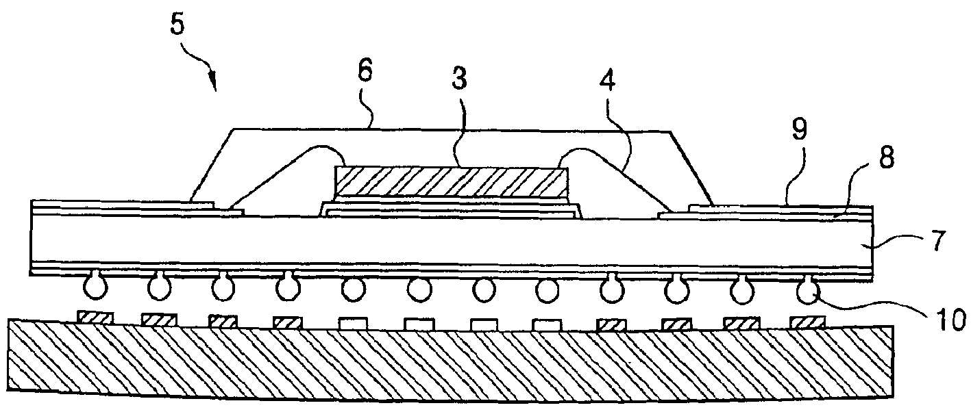
如图1所示,BGA封装5,作为SMT封装的例子,其组成为,陶瓷制成的或环氧树脂制成的衬底7,在衬底7上形成的电路图案8,涂在电路图案8上的焊接掩模9,装在衬底7中心的半导体芯片3,和将电路图案8和该半导体芯片3电连接的导线4。该半导体芯片3和导线4被覆盖有一层树脂层6以防止氧化和腐蚀。在面对印刷电路板51的衬底7的下表面具有多个焊球10与该衬底7电连接。该BGA封装5通过焊球10装在印刷电路板51上。As shown in Figure 1, the
在BGA封装5中,来自半导体芯片3的信号输出通过导线4传送给电路图案8。来自该电路图案8的信号通过焊球10传送到印刷电路板51,随后该信号传送给外围芯片(未示出)。另一方面,当信号从外围芯片传送到该半导体芯片3时,信号按逆向顺序传送。In the
如图3所示,焊球10提供在衬底7的下表面中心区以外的区域,具有固定间隔,而且每一个焊球10有着与其他焊球一样的尺寸。As shown in FIG. 3,
在印刷电路板51上具有多个对应焊球的位置的焊盘65以安装该BFA封装5,该焊盘65具有与焊球10的尺寸对应的统一尺寸。There are a plurality of
此外,在印刷电路板51上有迹线70,即,布线图,以便将BGA或CSP(芯片规模封装)电连接到装在印刷电路板51上的外围芯片。但是,很难将该迹线70与位于印刷电路板51内侧区域的焊盘65连接,因为焊盘65间的宽度非常窄,多条迹线70不易通过。因此,在多层印刷电路板51的情况下,建议在印刷电路板51的焊盘65内制作通孔的办法,这样,经通孔来连接迹线70和内侧焊盘65。In addition, on the printed
但是,因为印刷电路板51应具有通孔,并且随后形成有通孔的层的布线图案应该连接到装有该BGA封装5或CSP的层的布线图案,这样,印刷电路板的设计就变得复杂了。此外,如果该通孔不适合安放迹线70,焊盘65间的空间可以通过减小每一个焊盘65的尺寸来确保,以便在该空间内安放迹线70,但是在这种情况下,有一个问题,焊球10和焊盘65间的焊接状态就很糟糕了,因为用于连接焊盘65和焊球10的焊料减少了。However, since the printed
因此,在装有多个BGA或CSP的印刷电路板51的情况下,有必要在焊盘65间确保预定的空间。但是这降低了在印刷电路板51上安装外围芯片的整体水平。Therefore, in the case of the printed
发明内容Contents of the invention
因此,本发明的一个目的是提供一种印刷电路板,使其设计简单,提高外围芯片集成的数量,并保持良好的焊接状态。Therefore, an object of the present invention is to provide a printed circuit board which is simple in design, increases the number of peripheral chip integrations, and maintains a good soldering state.
本发明的另外一些目的和优点将在下面分部分进行说明,并且,有些部分通过说明变的很明显,或可以通过实施该发明来了解。Additional objects and advantages of the present invention will be described in sections below, and some parts will become obvious through the description, or can be learned by practicing the invention.
本发明的这些和其他的目的,可以通过提供具有多个对应做在半导体芯片封装上的焊接引脚的焊盘的印刷电路板来实现,该焊盘做在邻近印刷电路板的边缘的地方并具有朝向边缘方向延长的矩形形状。These and other objects of the present invention can be achieved by providing a printed circuit board having a plurality of pads corresponding to solder pins formed on a semiconductor chip package, the pads being made adjacent to the edge of the printed circuit board and Has a rectangular shape elongated toward the edges.
本发明的一个实施例中,邻近印刷电路板的中心区域的焊盘做成了圆形。In one embodiment of the present invention, the pads adjacent to the central area of the printed circuit board are formed in a circular shape.
本发明的一个实施例还具有,矩形焊盘的面积与圆形焊盘面积大致相同。An embodiment of the present invention also has that the area of the rectangular pad is approximately the same as that of the circular pad.
附图说明Description of drawings
本发明的这些和其他的目的和优势将通过结合附图进行的对于实施例的说明而变的明了和容易理解。These and other objects and advantages of the present invention will become clear and easy to understand through the description of the embodiments taken in conjunction with the accompanying drawings.
图1是具有多个引脚的芯片的示意截面图;Figure 1 is a schematic cross-sectional view of a chip with multiple pins;
图2是根据本发明的实施例的印刷电路板的平面图;和2 is a plan view of a printed circuit board according to an embodiment of the present invention; and
图3是传统的印刷电路板的平面图。Fig. 3 is a plan view of a conventional printed circuit board.
具体实施方式Detailed ways
下面将详细参考本发明的结合附图的详细的实施例,其中相同元件的标号是一致的。下述的实施例是为了结合附图解释本发明的。Reference will now be made in detail to the detailed embodiments of the present invention in conjunction with the accompanying drawings, wherein like elements are numbered identically. The following embodiments are for explaining the present invention with reference to the figures.
如图1所示,BGA(网格焊球阵列)封装,作为半导体芯片封装的例子被安装在根据本发明的印刷电路板上,该印刷电路板的组成为,环氧树脂制成的衬底7,在衬底7上形成的电路图案8,涂在电路图案8上的焊接掩模9,装在衬底7中心的半导体芯片3,和将电路图案8和该半导体芯片3电连接的导线4。该半导体芯片3和导线4被覆盖有一层树脂层6以防止氧化和腐蚀。As shown in FIG. 1, a BGA (Ball Grid Array) package, as an example of a semiconductor chip package, is mounted on a printed circuit board according to the present invention, which is composed of a substrate made of
在面对印刷电路板1(参照图2)的衬底7的下表面具有多个焊球10作为焊接引脚,它们与该衬底7电连接。焊球10以预定的间隔被做在衬底7的下表面上的中心区域以外的区域上以形成多个行和列。在此,每一个焊球10是半球状并彼此具有相同的尺寸。On the lower surface of the
如图2所示,在印刷电路板1上具有多个焊盘15以安装BGA封装5并与焊球10的位置对应。和焊球10一样,焊盘15以预定的间隔被安放在印刷电路板1上位于中心区域以外的区域上以形成多个行和列。As shown in FIG. 2 , there are a plurality of
在焊盘15中,邻近印刷电路板1的中心区的焊盘16为与传统的焊盘65类似的圆形,而邻近印刷电路板1的边缘的焊盘17为矩形。该矩形焊盘17从该印刷电路板1的中心向边缘延伸,最好是分别与圆形焊盘16的总面积相同。因此,该矩形焊盘17之间的宽度大于圆形焊盘16间的宽度。Among the
因此,由于焊盘17之间的宽度在该印刷电路板的边缘区域增加了,在矩形焊盘17间保证了安放迹线20的足够的空间。在此,迹线20通过连接到各自的焊盘15将该印刷电路板1与外围芯片连接在一起。此外,由于该矩形焊盘17在面积上等于圆形焊盘16,焊球10在每个矩形焊盘17的焊接状态与在每个圆形焊盘16的焊接状态等效。Therefore, since the width between the
另一方面,在该矩形焊盘17的各自的行在角区相遇时,由于安放迹线20有足够的空间,所以仍可以提供圆形焊盘16。On the other hand, when the respective rows of
如前所述,根据本发明,在安装了具有多个引脚例如焊球10的BGA封装或CSP的印刷电路板1上,邻近板的中心区域的焊盘16具有类似传统焊盘65的圆形,而邻近板的边缘的焊盘17为矩形。因此,安放连接邻近中心区域的焊盘16的迹线20的空间得到了保证,而不用形成通孔,这样就实现了对于印刷电路板的简单设计,并提高了在该印刷电路板1上对外围芯片的集成度。As previously described, according to the present invention, on a printed
在上述实施例中,邻近板的中心区域的焊盘16为圆形,但是也可以为邻近板的边缘的焊盘17的矩形,或其他具有本发明的功能的形状。In the above embodiments, the
如前所述,根据本发明,提供了一种印刷电路板,能够达到简单设计、提高安装外围芯片的集成度,并确保焊接状态。As mentioned above, according to the present invention, there is provided a printed circuit board capable of achieving a simple design, improving the integration of mounting peripheral chips, and ensuring a soldering state.
尽管揭示并描述了本发明的一些实施例,在不脱离本发明的原理和精神的条件下,该技术领域的技术人员可以对本发明的实施例进行修改。Although some embodiments of the present invention have been disclosed and described, those skilled in the art can make modifications to the embodiments of the present invention without departing from the principles and spirit of the present invention.
Claims (13)
Applications Claiming Priority (2)
| Application Number | Priority Date | Filing Date | Title |
|---|---|---|---|
| KR41547/2001 | 2001-07-11 | ||
| KR10-2001-0041547A KR100416000B1 (en) | 2001-07-11 | 2001-07-11 | Pcb mounting chip having plural pins |
Publications (2)
| Publication Number | Publication Date |
|---|---|
| CN1396799A CN1396799A (en) | 2003-02-12 |
| CN1248552C true CN1248552C (en) | 2006-03-29 |
Family
ID=19712044
Family Applications (1)
| Application Number | Title | Priority Date | Filing Date |
|---|---|---|---|
| CNB021222908A Expired - Fee Related CN1248552C (en) | 2001-07-11 | 2002-06-04 | Printed circuit board with improved pad structure |
Country Status (3)
| Country | Link |
|---|---|
| US (1) | US7199478B2 (en) |
| KR (1) | KR100416000B1 (en) |
| CN (1) | CN1248552C (en) |
Families Citing this family (22)
| Publication number | Priority date | Publication date | Assignee | Title |
|---|---|---|---|---|
| DE10157362B4 (en) * | 2001-11-23 | 2006-11-16 | Infineon Technologies Ag | Power module and method for its production |
| JP2005166794A (en) | 2003-12-01 | 2005-06-23 | Ricoh Co Ltd | Component package, printed wiring board and electronic equipment |
| CN100369533C (en) * | 2004-01-18 | 2008-02-13 | 敦南科技股份有限公司 | Wire bonding method for circuit board packaging |
| KR100632469B1 (en) | 2004-04-20 | 2006-10-09 | 삼성전자주식회사 | Semiconductor chip package |
| CN1314509C (en) * | 2004-11-24 | 2007-05-09 | 广州金升阳科技有限公司 | Pad spot welding method |
| US7425684B2 (en) * | 2005-02-03 | 2008-09-16 | Sang Henry Ta | Universal systems printed circuit board for interconnections |
| US20060172614A1 (en) * | 2005-02-03 | 2006-08-03 | Ta Sang H | Universal systems printed circuit blocks and method for interconnecting the same |
| USD600219S1 (en) * | 2006-04-26 | 2009-09-15 | Panasonic Corporation | Lead frame |
| US7962232B2 (en) * | 2006-10-01 | 2011-06-14 | Dell Products L.P. | Methods and media for processing a circuit board |
| JP5049573B2 (en) * | 2006-12-12 | 2012-10-17 | 新光電気工業株式会社 | Semiconductor device |
| JP2009182104A (en) * | 2008-01-30 | 2009-08-13 | Toshiba Corp | Semiconductor package |
| FR2967328B1 (en) * | 2010-11-10 | 2012-12-21 | Sierra Wireless Inc | ELECTRONIC CIRCUIT COMPRISING A FACE OF REPORT ON WHICH ARE AGENCIES OF CONTACT PLOTS |
| JP5842859B2 (en) * | 2013-04-15 | 2016-01-13 | 株式会社村田製作所 | Multilayer wiring board and module having the same |
| KR102041501B1 (en) * | 2013-09-13 | 2019-11-06 | 삼성전자 주식회사 | Array printed circuit board, method for replacing X-out printed circuit board of the same and electronic apparatus using the same |
| CN105188257B (en) * | 2015-08-31 | 2018-06-19 | 广东欧珀移动通信有限公司 | Circuit board and its electronic product and chip recognition methods |
| CN107612226B (en) * | 2017-10-31 | 2024-05-03 | 珠海格力电器股份有限公司 | Surface mounting structure, surface mounting method, motor and surface mounting chip |
| CN212064501U (en) * | 2020-03-13 | 2020-12-01 | 华为技术有限公司 | Circuit board structure and electronic equipment |
| CN112752398A (en) * | 2020-11-24 | 2021-05-04 | 广州朗国电子科技有限公司 | Chip bonding pad structure of PCB |
| CN115279024A (en) * | 2021-11-16 | 2022-11-01 | 天芯互联科技有限公司 | Circuit board and circuit board processing method |
| CN114464585B (en) * | 2022-04-12 | 2022-07-12 | 飞腾信息技术有限公司 | Semiconductor substrate, semiconductor device, integrated circuit system and electronic equipment |
| CN114501849A (en) * | 2022-04-15 | 2022-05-13 | 北京万龙精益科技有限公司 | Improved design method of integrated circuit packaging bonding pad and bonding pad packaging library |
| KR20240011486A (en) * | 2022-07-19 | 2024-01-26 | 삼성전자주식회사 | Substrate |
Family Cites Families (23)
| Publication number | Priority date | Publication date | Assignee | Title |
|---|---|---|---|---|
| US4720915A (en) * | 1986-03-25 | 1988-01-26 | True Grid, Ltd. | Printed circuit board and process for its manufacture |
| JPH04241676A (en) * | 1991-01-16 | 1992-08-28 | Nec Corp | Pattern data structure of printed wiring board |
| US5194137A (en) * | 1991-08-05 | 1993-03-16 | Motorola Inc. | Solder plate reflow method for forming solder-bumped terminals |
| US5340772A (en) * | 1992-07-17 | 1994-08-23 | Lsi Logic Corporation | Method of increasing the layout efficiency of dies on a wafer and increasing the ratio of I/O area to active area per die |
| US5593927A (en) * | 1993-10-14 | 1997-01-14 | Micron Technology, Inc. | Method for packaging semiconductor dice |
| US5557505A (en) * | 1994-07-22 | 1996-09-17 | Ast Research, Inc. | Dual pattern microprocessor package footprint |
| JPH08274425A (en) * | 1995-03-29 | 1996-10-18 | Sony Corp | Printed wiring board |
| US5829124A (en) * | 1995-12-29 | 1998-11-03 | International Business Machines Corporation | Method for forming metallized patterns on the top surface of a printed circuit board |
| EP0817548B1 (en) * | 1996-01-11 | 2006-04-05 | Ibiden Co., Ltd. | Printed wiring board and method for manufacturing the same |
| JP2825085B2 (en) * | 1996-08-29 | 1998-11-18 | 日本電気株式会社 | Semiconductor device mounting structure, mounting board, and mounting state inspection method |
| JPH10290058A (en) * | 1997-04-16 | 1998-10-27 | Seiko Epson Corp | Printed board |
| JPH116103A (en) | 1997-06-18 | 1999-01-12 | Maeda Road Constr Co Ltd | Soil pavement material, soil pavement mechanism, and conditioning method for raw material for soil pavement |
| JPH1126919A (en) * | 1997-06-30 | 1999-01-29 | Fuji Photo Film Co Ltd | Printed wiring board |
| US6333565B1 (en) * | 1998-03-23 | 2001-12-25 | Seiko Epson Corporation | Semiconductor device and method of manufacturing the same, circuit board, and electronic instrument |
| US6316736B1 (en) * | 1998-06-08 | 2001-11-13 | Visteon Global Technologies, Inc. | Anti-bridging solder ball collection zones |
| US6118182A (en) | 1998-06-25 | 2000-09-12 | Intel Corporation | Integrated circuit package with rectangular contact pads |
| JP2000077819A (en) * | 1998-08-31 | 2000-03-14 | Toshiba Corp | Printed circuit boards and electronic units |
| JP2000244106A (en) | 1998-12-25 | 2000-09-08 | Ibiden Co Ltd | Substrate for mounting electronic components |
| JP2000208909A (en) | 1999-01-12 | 2000-07-28 | Nec Home Electronics Ltd | Printed board |
| JP2000223653A (en) * | 1999-02-02 | 2000-08-11 | Rohm Co Ltd | Semiconductor device having chip-on-chip structure and semiconductor chip used therefor |
| KR100347949B1 (en) * | 1999-11-27 | 2002-08-09 | 엘지전자주식회사 | A structure of solder land for component mounting |
| US20020144397A1 (en) * | 2000-01-21 | 2002-10-10 | Morris Terrel L. | Subtractive process for fabricating cylindrical printed circuit boards |
| JP2001320154A (en) * | 2000-05-02 | 2001-11-16 | Satsuma Tsushin Kogyo Kk | Method and apparatus for filling liquid resin to fill through-hole substrate |
-
2001
- 2001-07-11 KR KR10-2001-0041547A patent/KR100416000B1/en not_active Expired - Fee Related
-
2002
- 2002-05-29 US US10/156,016 patent/US7199478B2/en not_active Expired - Fee Related
- 2002-06-04 CN CNB021222908A patent/CN1248552C/en not_active Expired - Fee Related
Also Published As
| Publication number | Publication date |
|---|---|
| KR100416000B1 (en) | 2004-01-24 |
| KR20030006008A (en) | 2003-01-23 |
| CN1396799A (en) | 2003-02-12 |
| US20030011074A1 (en) | 2003-01-16 |
| US7199478B2 (en) | 2007-04-03 |
Similar Documents
| Publication | Publication Date | Title |
|---|---|---|
| CN1248552C (en) | Printed circuit board with improved pad structure | |
| TWI399146B (en) | Printed circuit board, manufacturing method thereof and ball grid array land pattern | |
| US6549421B2 (en) | Stackable ball grid array package | |
| US7671478B2 (en) | Low height vertical sensor packaging | |
| JPH11297889A (en) | Semiconductor package and mounting substrate, and mounting method using the same | |
| US5450289A (en) | Semiconductor package and a printed circuit board applicable to its mounting | |
| US7180182B2 (en) | Semiconductor component | |
| US6320249B1 (en) | Multiple line grids incorporating therein circuit elements | |
| US6054757A (en) | Semiconductor apparatus, circuit board and combination thereof | |
| US6657133B1 (en) | Ball grid array chip capacitor structure | |
| KR100850286B1 (en) | Semiconductor chip package equipped with an electronic device and integrated circuit module having the same | |
| US20030080418A1 (en) | Semiconductor device having power supply pads arranged between signal pads and substrate edge | |
| CN1324108A (en) | Multiple line grid for application of packaging or testing | |
| KR100233864B1 (en) | Input and output bump forming method of area array bumped semiconductor package using lead frame | |
| EP4429413B1 (en) | Thermally improved substrate structure and package assembly with the same | |
| KR100367729B1 (en) | Multiple line grid array package | |
| KR100720410B1 (en) | Substrates for Semiconductor Packages with Passive Elements | |
| KR100196992B1 (en) | Lead frame and chip scale package having it | |
| JP4523425B2 (en) | Semiconductor device mounting substrate | |
| JPH02138766A (en) | Package structure of electronic component | |
| JP2001210785A (en) | Semiconductor integrated circuit mounting method and mounting case | |
| KR20110071669A (en) | Flip chip package | |
| JPH02249260A (en) | Semiconductor package and circuit device mounting same | |
| KR20000011420U (en) | Stacked Semiconductor Packages | |
| HK1129524B (en) | A pcb and the method of making it and ball grid array pad pattern |
Legal Events
| Date | Code | Title | Description |
|---|---|---|---|
| C10 | Entry into substantive examination | ||
| SE01 | Entry into force of request for substantive examination | ||
| C06 | Publication | ||
| PB01 | Publication | ||
| C10 | Entry into substantive examination | ||
| SE01 | Entry into force of request for substantive examination | ||
| C14 | Grant of patent or utility model | ||
| GR01 | Patent grant | ||
| CF01 | Termination of patent right due to non-payment of annual fee |
Granted publication date: 20060329 Termination date: 20160604 |