CN1249780C - Method for growing GaN crystal chip and GaN crystal chip - Google Patents
Method for growing GaN crystal chip and GaN crystal chip Download PDFInfo
- Publication number
- CN1249780C CN1249780C CNB021078866A CN02107886A CN1249780C CN 1249780 C CN1249780 C CN 1249780C CN B021078866 A CNB021078866 A CN B021078866A CN 02107886 A CN02107886 A CN 02107886A CN 1249780 C CN1249780 C CN 1249780C
- Authority
- CN
- China
- Prior art keywords
- gan
- substrate
- film
- metal film
- metal
- Prior art date
- Legal status (The legal status is an assumption and is not a legal conclusion. Google has not performed a legal analysis and makes no representation as to the accuracy of the status listed.)
- Expired - Fee Related
Links
Images


Classifications
-
- H—ELECTRICITY
- H10—SEMICONDUCTOR DEVICES; ELECTRIC SOLID-STATE DEVICES NOT OTHERWISE PROVIDED FOR
- H10P—GENERIC PROCESSES OR APPARATUS FOR THE MANUFACTURE OR TREATMENT OF DEVICES COVERED BY CLASS H10
- H10P14/00—Formation of materials, e.g. in the shape of layers or pillars
- H10P14/20—Formation of materials, e.g. in the shape of layers or pillars of semiconductor materials
- H10P14/32—Formation of materials, e.g. in the shape of layers or pillars of semiconductor materials characterised by intermediate layers between substrates and deposited layers
- H10P14/3202—Materials thereof
- H10P14/3241—Materials thereof being conductive materials
-
- C—CHEMISTRY; METALLURGY
- C30—CRYSTAL GROWTH
- C30B—SINGLE-CRYSTAL GROWTH; UNIDIRECTIONAL SOLIDIFICATION OF EUTECTIC MATERIAL OR UNIDIRECTIONAL DEMIXING OF EUTECTOID MATERIAL; REFINING BY ZONE-MELTING OF MATERIAL; PRODUCTION OF A HOMOGENEOUS POLYCRYSTALLINE MATERIAL WITH DEFINED STRUCTURE; SINGLE CRYSTALS OR HOMOGENEOUS POLYCRYSTALLINE MATERIAL WITH DEFINED STRUCTURE; AFTER-TREATMENT OF SINGLE CRYSTALS OR A HOMOGENEOUS POLYCRYSTALLINE MATERIAL WITH DEFINED STRUCTURE; APPARATUS THEREFOR
- C30B25/00—Single-crystal growth by chemical reaction of reactive gases, e.g. chemical vapour-deposition growth
- C30B25/02—Epitaxial-layer growth
-
- C—CHEMISTRY; METALLURGY
- C30—CRYSTAL GROWTH
- C30B—SINGLE-CRYSTAL GROWTH; UNIDIRECTIONAL SOLIDIFICATION OF EUTECTIC MATERIAL OR UNIDIRECTIONAL DEMIXING OF EUTECTOID MATERIAL; REFINING BY ZONE-MELTING OF MATERIAL; PRODUCTION OF A HOMOGENEOUS POLYCRYSTALLINE MATERIAL WITH DEFINED STRUCTURE; SINGLE CRYSTALS OR HOMOGENEOUS POLYCRYSTALLINE MATERIAL WITH DEFINED STRUCTURE; AFTER-TREATMENT OF SINGLE CRYSTALS OR A HOMOGENEOUS POLYCRYSTALLINE MATERIAL WITH DEFINED STRUCTURE; APPARATUS THEREFOR
- C30B25/00—Single-crystal growth by chemical reaction of reactive gases, e.g. chemical vapour-deposition growth
- C30B25/02—Epitaxial-layer growth
- C30B25/18—Epitaxial-layer growth characterised by the substrate
-
- C—CHEMISTRY; METALLURGY
- C30—CRYSTAL GROWTH
- C30B—SINGLE-CRYSTAL GROWTH; UNIDIRECTIONAL SOLIDIFICATION OF EUTECTIC MATERIAL OR UNIDIRECTIONAL DEMIXING OF EUTECTOID MATERIAL; REFINING BY ZONE-MELTING OF MATERIAL; PRODUCTION OF A HOMOGENEOUS POLYCRYSTALLINE MATERIAL WITH DEFINED STRUCTURE; SINGLE CRYSTALS OR HOMOGENEOUS POLYCRYSTALLINE MATERIAL WITH DEFINED STRUCTURE; AFTER-TREATMENT OF SINGLE CRYSTALS OR A HOMOGENEOUS POLYCRYSTALLINE MATERIAL WITH DEFINED STRUCTURE; APPARATUS THEREFOR
- C30B29/00—Single crystals or homogeneous polycrystalline material with defined structure characterised by the material or by their shape
- C30B29/10—Inorganic compounds or compositions
- C30B29/40—AIIIBV compounds wherein A is B, Al, Ga, In or Tl and B is N, P, As, Sb or Bi
-
- C—CHEMISTRY; METALLURGY
- C30—CRYSTAL GROWTH
- C30B—SINGLE-CRYSTAL GROWTH; UNIDIRECTIONAL SOLIDIFICATION OF EUTECTIC MATERIAL OR UNIDIRECTIONAL DEMIXING OF EUTECTOID MATERIAL; REFINING BY ZONE-MELTING OF MATERIAL; PRODUCTION OF A HOMOGENEOUS POLYCRYSTALLINE MATERIAL WITH DEFINED STRUCTURE; SINGLE CRYSTALS OR HOMOGENEOUS POLYCRYSTALLINE MATERIAL WITH DEFINED STRUCTURE; AFTER-TREATMENT OF SINGLE CRYSTALS OR A HOMOGENEOUS POLYCRYSTALLINE MATERIAL WITH DEFINED STRUCTURE; APPARATUS THEREFOR
- C30B29/00—Single crystals or homogeneous polycrystalline material with defined structure characterised by the material or by their shape
- C30B29/10—Inorganic compounds or compositions
- C30B29/40—AIIIBV compounds wherein A is B, Al, Ga, In or Tl and B is N, P, As, Sb or Bi
- C30B29/403—AIII-nitrides
- C30B29/406—Gallium nitride
-
- H—ELECTRICITY
- H10—SEMICONDUCTOR DEVICES; ELECTRIC SOLID-STATE DEVICES NOT OTHERWISE PROVIDED FOR
- H10P—GENERIC PROCESSES OR APPARATUS FOR THE MANUFACTURE OR TREATMENT OF DEVICES COVERED BY CLASS H10
- H10P14/00—Formation of materials, e.g. in the shape of layers or pillars
- H10P14/20—Formation of materials, e.g. in the shape of layers or pillars of semiconductor materials
- H10P14/27—Formation of materials, e.g. in the shape of layers or pillars of semiconductor materials using selective deposition, e.g. simultaneous growth of monocrystalline and non-monocrystalline semiconductor materials
-
- H—ELECTRICITY
- H10—SEMICONDUCTOR DEVICES; ELECTRIC SOLID-STATE DEVICES NOT OTHERWISE PROVIDED FOR
- H10P—GENERIC PROCESSES OR APPARATUS FOR THE MANUFACTURE OR TREATMENT OF DEVICES COVERED BY CLASS H10
- H10P14/00—Formation of materials, e.g. in the shape of layers or pillars
- H10P14/20—Formation of materials, e.g. in the shape of layers or pillars of semiconductor materials
- H10P14/29—Formation of materials, e.g. in the shape of layers or pillars of semiconductor materials characterised by the substrates
- H10P14/2901—Materials
- H10P14/2902—Materials being Group IVA materials
- H10P14/2905—Silicon, silicon germanium or germanium
-
- H—ELECTRICITY
- H10—SEMICONDUCTOR DEVICES; ELECTRIC SOLID-STATE DEVICES NOT OTHERWISE PROVIDED FOR
- H10P—GENERIC PROCESSES OR APPARATUS FOR THE MANUFACTURE OR TREATMENT OF DEVICES COVERED BY CLASS H10
- H10P14/00—Formation of materials, e.g. in the shape of layers or pillars
- H10P14/20—Formation of materials, e.g. in the shape of layers or pillars of semiconductor materials
- H10P14/29—Formation of materials, e.g. in the shape of layers or pillars of semiconductor materials characterised by the substrates
- H10P14/2901—Materials
- H10P14/2907—Materials being Group IIIA-VA materials
- H10P14/2908—Nitrides
-
- H—ELECTRICITY
- H10—SEMICONDUCTOR DEVICES; ELECTRIC SOLID-STATE DEVICES NOT OTHERWISE PROVIDED FOR
- H10P—GENERIC PROCESSES OR APPARATUS FOR THE MANUFACTURE OR TREATMENT OF DEVICES COVERED BY CLASS H10
- H10P14/00—Formation of materials, e.g. in the shape of layers or pillars
- H10P14/20—Formation of materials, e.g. in the shape of layers or pillars of semiconductor materials
- H10P14/29—Formation of materials, e.g. in the shape of layers or pillars of semiconductor materials characterised by the substrates
- H10P14/2901—Materials
- H10P14/2921—Materials being crystalline insulating materials
-
- H—ELECTRICITY
- H10—SEMICONDUCTOR DEVICES; ELECTRIC SOLID-STATE DEVICES NOT OTHERWISE PROVIDED FOR
- H10P—GENERIC PROCESSES OR APPARATUS FOR THE MANUFACTURE OR TREATMENT OF DEVICES COVERED BY CLASS H10
- H10P14/00—Formation of materials, e.g. in the shape of layers or pillars
- H10P14/20—Formation of materials, e.g. in the shape of layers or pillars of semiconductor materials
- H10P14/32—Formation of materials, e.g. in the shape of layers or pillars of semiconductor materials characterised by intermediate layers between substrates and deposited layers
- H10P14/3202—Materials thereof
- H10P14/3214—Materials thereof being Group IIIA-VA semiconductors
- H10P14/3216—Nitrides
-
- H—ELECTRICITY
- H10—SEMICONDUCTOR DEVICES; ELECTRIC SOLID-STATE DEVICES NOT OTHERWISE PROVIDED FOR
- H10P—GENERIC PROCESSES OR APPARATUS FOR THE MANUFACTURE OR TREATMENT OF DEVICES COVERED BY CLASS H10
- H10P14/00—Formation of materials, e.g. in the shape of layers or pillars
- H10P14/20—Formation of materials, e.g. in the shape of layers or pillars of semiconductor materials
- H10P14/32—Formation of materials, e.g. in the shape of layers or pillars of semiconductor materials characterised by intermediate layers between substrates and deposited layers
- H10P14/3242—Structure
- H10P14/3244—Layer structure
- H10P14/3248—Layer structure consisting of two layers
-
- H—ELECTRICITY
- H10—SEMICONDUCTOR DEVICES; ELECTRIC SOLID-STATE DEVICES NOT OTHERWISE PROVIDED FOR
- H10P—GENERIC PROCESSES OR APPARATUS FOR THE MANUFACTURE OR TREATMENT OF DEVICES COVERED BY CLASS H10
- H10P14/00—Formation of materials, e.g. in the shape of layers or pillars
- H10P14/20—Formation of materials, e.g. in the shape of layers or pillars of semiconductor materials
- H10P14/34—Deposited materials, e.g. layers
- H10P14/3402—Deposited materials, e.g. layers characterised by the chemical composition
- H10P14/3414—Deposited materials, e.g. layers characterised by the chemical composition being group IIIA-VIA materials
- H10P14/3416—Nitrides
-
- Y—GENERAL TAGGING OF NEW TECHNOLOGICAL DEVELOPMENTS; GENERAL TAGGING OF CROSS-SECTIONAL TECHNOLOGIES SPANNING OVER SEVERAL SECTIONS OF THE IPC; TECHNICAL SUBJECTS COVERED BY FORMER USPC CROSS-REFERENCE ART COLLECTIONS [XRACs] AND DIGESTS
- Y10—TECHNICAL SUBJECTS COVERED BY FORMER USPC
- Y10S—TECHNICAL SUBJECTS COVERED BY FORMER USPC CROSS-REFERENCE ART COLLECTIONS [XRACs] AND DIGESTS
- Y10S117/00—Single-crystal, oriented-crystal, and epitaxy growth processes; non-coating apparatus therefor
- Y10S117/915—Separating from substrate
Landscapes
- Chemical & Material Sciences (AREA)
- Engineering & Computer Science (AREA)
- Crystallography & Structural Chemistry (AREA)
- Materials Engineering (AREA)
- Metallurgy (AREA)
- Organic Chemistry (AREA)
- Chemical Kinetics & Catalysis (AREA)
- General Chemical & Material Sciences (AREA)
- Inorganic Chemistry (AREA)
- Crystals, And After-Treatments Of Crystals (AREA)
- Semiconductor Lasers (AREA)
- Led Devices (AREA)
Abstract
在初始衬底上沉积金属膜,初始衬底可以是单晶蓝宝石衬底、带有生长在蓝宝石衬底上的单晶GaN膜的衬底或单晶半导体衬底中的任何一种。然后在金属膜上沉积GaN膜以形成层状衬底。由于采用了以上这种结构,在生长了GaN膜之后,GaN膜可以很容易地和初始衬底分开,并且,能够用简单的方式生产出来低缺陷浓度和没有被杂质严重污染的GaN晶体衬底。
A metal film is deposited on an initial substrate, which may be any one of a single crystal sapphire substrate, a substrate with a single crystal GaN film grown on a sapphire substrate, or a single crystal semiconductor substrate. A GaN film is then deposited on the metal film to form a layered substrate. Due to the adoption of the above structure, after the GaN film is grown, the GaN film can be easily separated from the initial substrate, and a GaN crystal substrate with low defect concentration and not heavily contaminated by impurities can be produced in a simple manner. .
Description
技术领域technical field
本发明涉及生长GaN晶体衬底的方法及GaN晶体衬底。The invention relates to a method for growing a GaN crystal substrate and a GaN crystal substrate.
背景技术Background technique
GaN复合半导体,例如GaN、InGaN和GaAlN,作为可用作蓝光发光二极管(LEDs)和激光二极管(LDs)的材料已经引起了注意。此外,由于很好的耐热性和环境抵抗能力,GaN复合半导体在光学设备中得到了运用,同样由于这些特性,GaN还用于电子元器件的发展。GaN compound semiconductors, such as GaN, InGaN, and GaAlN, have attracted attention as materials that can be used as blue light-emitting diodes (LEDs) and laser diodes (LDs). In addition, GaN compound semiconductors are used in optical devices due to their excellent heat resistance and environmental resistance, and GaN is also used in the development of electronic components due to these characteristics.
然而,很难生长出大的GaN复合半导体晶体,并且由于这个原因,还没有生产出来有实际用途的GaN衬底。蓝宝石作为生长GaN的衬底在目前已经得到广泛的实际应用,并且在单晶蓝宝石衬底上外延生长GaN是一种很普遍的方法,例如,运用金属有机物气相外延法。However, it is difficult to grow large GaN compound semiconductor crystals, and for this reason, GaN substrates for practical use have not yet been produced. Sapphire as a substrate for growing GaN has been widely used in practice at present, and epitaxial growth of GaN on a single crystal sapphire substrate is a very common method, for example, using metal organic vapor phase epitaxy.
蓝宝石衬底和GaN的晶格常数不同,因此,当直接在蓝宝石衬底上生长GaN时,生长不出单晶GaN薄膜。为了解决这个问题,日本专利(公开号:No.188983/1988)公开了一种方法,先在蓝宝石衬底上低温生长AlN或者GaN的缓冲层以减小晶格应变,然后在缓冲层上生长GaN。The lattice constants of the sapphire substrate and GaN are different, therefore, when GaN is grown directly on the sapphire substrate, no single crystal GaN film can be grown. In order to solve this problem, Japanese patent (publication number: No.188983/1988) discloses a method, first grows the buffer layer of AlN or GaN on the sapphire substrate at low temperature to reduce the lattice strain, and then grows on the buffer layer GaN.
然而,即使在用低温生长的缓冲层来长GaN时,衬底和GaN晶体的晶格常数也会产生差异,并且因而导致GaN会有许多缺陷,这些缺陷被认为在生产GaN基的激光二极管时是一个障碍。此外,由于蓝宝石和GaN线性膨胀系数的差异,在外延后的衬底中会产生扭曲,在最坏的情况下,衬底会很不利地破裂。However, even when GaN is grown with a low-temperature-grown buffer layer, differences in the lattice constants of the substrate and the GaN crystal occur, and thus GaN has many defects that are thought to be critical in the production of GaN-based laser diodes. is a hindrance. Furthermore, due to the difference in the linear expansion coefficients of sapphire and GaN, distortions can be generated in the epitaxial substrate, and in the worst case, the substrate can be unfavorably cracked.
由于这个原因,人们正热切地期待着发展出大的GaN衬底。For this reason, the development of large GaN substrates is eagerly anticipated.
虽然生长大的GaN晶体非常困难,但是近来已提出了一种在衬底上异质外延生长GaN厚膜的方法,例如,HVPE(氢化物气相外延)方法,当衬底被除去后就会得到一种自由固定的GaN衬底。Although it is very difficult to grow large GaN crystals, a method for heteroepitaxially growing GaN thick films on substrates has recently been proposed, for example, the HVPE (Hydride Vapor Phase Epitaxy) method, when the substrate is removed to obtain A freely fixed GaN substrate.
顺便说一下,在目前,还没有发展出任何可通过蚀刻来分离GaN和蓝宝石衬底的技术。虽然已尝试通过抛光来机械地除去蓝宝石衬底,但是在磨光的工艺中会增加衬底的扭曲,并且,衬底破裂的可能性也会增加。由于这个原因,这种方法还没有被付诸于实际运用。By the way, at present, no technique has been developed to separate GaN and sapphire substrates by etching. Although attempts have been made to mechanically remove the sapphire substrate by polishing, substrate distortion is increased during the polishing process, and the likelihood of substrate cracking also increases. For this reason, this method has not been put into practical use.
在此,Jpn.J.Appl.Phys.Vol.38(1999)Pt.2,No.3A上报道了一种方法:在运用HVPE方法于蓝宝石衬底上生成了厚的GaN膜以后,用激光脉冲分离GaN膜。然而,这种方法也可能引起衬底的破裂。Here, a method is reported in Jpn.J.Appl.Phys.Vol.38(1999)Pt.2, No.3A: After using the HVPE method to form a thick GaN film on a sapphire substrate, use laser Pulse detaches the GaN film. However, this method may also cause cracking of the substrate.
此外,日本专利(公开号:No.12900/2000)公开了一种利用很容易除去的衬底的方法。在这种方法中,通过HVPE方法先在GaAs衬底上生长一层很厚的GaN膜,然后用蚀刻的方法除去GaAs衬底。使用这种方法,可以以相对较高的产量制备大的GaN衬底。然而,这种方法存在一个问题,那就是GaAs衬底在GaN晶体生长的工艺中会很不利地分解,并且As会作为杂质存在于GaN中。Furthermore, Japanese Patent (Kokai Publication No. 12900/2000) discloses a method using an easily removable substrate. In this method, a thick GaN film is first grown on the GaAs substrate by HVPE method, and then the GaAs substrate is removed by etching. Using this method, large GaN substrates can be fabricated with relatively high yields. However, this method has a problem in that the GaAs substrate is unfavorably decomposed during the GaN crystal growth process, and As exists in GaN as an impurity.
运用掩模技术选择生长可有效地减小外延生长的GaN的缺陷浓度,例如,日本专利(公开号:No.312971/1998)公开了一种这样的技术。然而,因为没有很容易分离衬底的方法,以上的技术不能被有效的用于生产自由固定的GaN衬底。Selective growth using a mask technique can effectively reduce the defect concentration of epitaxially grown GaN. For example, Japanese Patent (Kokai Publication No. 312971/1998) discloses such a technique. However, the above techniques cannot be effectively used to produce free-fixed GaN substrates because there is no easy way to separate the substrates.
发明内容Contents of the invention
因此,本发明的目的之一是解决以前工艺的问题,并提供一个通过简单方法而生产出低缺陷浓度和不被杂质严重污染的GaN晶体衬底,以及提供由本方法生产的GaN晶体衬底。Accordingly, one of the objects of the present invention is to solve the problems of the prior art and to provide a GaN crystal substrate which is produced by a simple method with a low defect concentration and which is not heavily contaminated by impurities, and to provide a GaN crystal substrate produced by the method.
根据本发明的第一个方面,生产GaN晶体衬底的工艺包括这些步骤:According to a first aspect of the present invention, the process for producing a GaN crystal substrate includes the steps of:
在初始衬底上沉积一层金属膜,初始衬底可以是单晶蓝宝石衬底、带有在蓝宝石衬底上生长的单晶GaN膜的衬底或单晶半导体衬底中的任何一种。A metal film is deposited on the initial substrate, which may be any one of a single crystal sapphire substrate, a substrate with a single crystal GaN film grown on the sapphire substrate, or a single crystal semiconductor substrate.
在金属膜上沉积一层GaN膜用于形成层状衬底;并且depositing a GaN film on the metal film to form a layered substrate; and
把初始衬底从沉积了GaN的层状衬底上除去,从而形成了自由固定的GaN晶体衬底。The initial substrate was removed from the GaN-deposited layered substrate, thereby forming a freely fixed GaN crystal substrate.
根据本发明的第二个方面,生产GaN晶体衬底的工艺包括这些步骤:According to a second aspect of the present invention, the process for producing a GaN crystal substrate includes the steps of:
在初始衬底上沉积一层金属膜,初始衬底可以是单晶蓝宝石衬底、带有在蓝宝石衬底上生长的单晶GaN膜的衬底或单晶半导体衬底中的任何一种。A metal film is deposited on the initial substrate, which may be any one of a single crystal sapphire substrate, a substrate with a single crystal GaN film grown on the sapphire substrate, or a single crystal semiconductor substrate.
在金属膜上由掩模材料形成掩模区和GaN选择生长区;forming a mask region and a GaN selective growth region on the metal film by using a mask material;
把选择生长区作为源,在选择生长区和掩模区沉积GaN膜以形成层状衬底;并且using the selective growth region as a source, depositing a GaN film on the selective growth region and the masked region to form a layered substrate; and
把初始衬底从沉积了GaN的层状衬底上除去,从而形成了自由固定的GaN晶体衬底。The initial substrate was removed from the GaN-deposited layered substrate, thereby forming a freely fixed GaN crystal substrate.
根据本发明的第三个方面,生产GaN晶体衬底的工艺包括这些步骤:According to a third aspect of the present invention, the process for producing a GaN crystal substrate includes the steps of:
在初始衬底上沉积一层金属膜,初始衬底可以是单晶蓝宝石衬底、带有在蓝宝石衬底上生长的单晶GaN膜的衬底或单晶半导体衬底中的任何一种。A metal film is deposited on the initial substrate, which may be any one of a single crystal sapphire substrate, a substrate with a single crystal GaN film grown on the sapphire substrate, or a single crystal semiconductor substrate.
在金属膜上沉积GaN膜;Depositing a GaN film on the metal film;
在GaN膜上由掩模材料形成掩模区和GaN选择生长区;forming a mask region and a GaN selective growth region on the GaN film by using a mask material;
把选择生长区作为源,在选择生长区和掩模区沉积GaN膜以形成层状衬底;并且using the selective growth region as a source, depositing a GaN film on the selective growth region and the masked region to form a layered substrate; and
把初始衬底从沉积了GaN的层状衬底上除去,从而形成了自由固定的GaN晶体衬底。The initial substrate was removed from the GaN-deposited layered substrate, thereby forming a freely fixed GaN crystal substrate.
根据本发明的第四个方面,生产GaN晶体衬底的工艺包括这些步骤:According to a fourth aspect of the present invention, the process for producing a GaN crystal substrate includes the steps of:
在初始衬底上由掩模材料形成掩模区和GaN选择生长区,初始衬底可以是单晶蓝宝石衬底、带有在蓝宝石衬底上生长的单晶GaN膜的衬底或单晶半导体衬底中的任何一种。A mask region and a GaN selective growth region are formed by a mask material on the initial substrate, which can be a single crystal sapphire substrate, a substrate with a single crystal GaN film grown on a sapphire substrate, or a single crystal semiconductor any of the substrates.
把选择生长区作为源,在选择生长区和掩模区沉积GaN膜;Using the selective growth region as a source, depositing a GaN film on the selective growth region and the mask region;
在GaN膜上形成金属膜;Forming a metal film on the GaN film;
在金属膜上再一次沉积GaN膜以形成层状衬底;并且Depositing a GaN film again on the metal film to form a layered substrate; and
把初始衬底从又一次沉积了GaN的层状衬底上除去,从而形成了自由固定的GaN晶体衬底。The initial substrate was removed from the layered substrate on which GaN was again deposited, thereby forming a freely fixed GaN crystal substrate.
根据这项具有上述各自结构的发明的第一到第四个方面,生产工艺可能会进一步包括下面的步骤:According to the first to fourth aspects of the invention having the above respective structures, the production process may further include the following steps:
在自由固定的GaN初始晶体衬底上沉积一层金属膜;Deposit a metal film on the freely fixed GaN initial crystal substrate;
在金属膜上沉积GaN膜以形成层状衬底;并且depositing a GaN film on the metal film to form a layered substrate; and
把初始衬底从沉积了GaN的层状衬底上除去,从而形成了自由固定的GaN晶体衬底。The initial substrate was removed from the GaN-deposited layered substrate, thereby forming a freely fixed GaN crystal substrate.
根据这项具有上述各自结构的发明的第一到第四个方面,生产工艺可能会进一步包括下面的步骤:According to the first to fourth aspects of the invention having the above respective structures, the production process may further include the following steps:
在自由固定的GaN初始晶体衬底上沉积一层金属膜;Deposit a metal film on the freely fixed GaN initial crystal substrate;
在金属膜上由掩模材料形成掩模区和GaN选择生长区;forming a mask region and a GaN selective growth region on the metal film by using a mask material;
把选择生长区作为源,在选择生长区和掩模区沉积GaN膜以形成层状衬底;并且using the selective growth region as a source, depositing a GaN film on the selective growth region and the masked region to form a layered substrate; and
把初始衬底从沉积了GaN的层状衬底上除去,从而形成了自由固定的GaN晶体衬底。The initial substrate was removed from the GaN-deposited layered substrate, thereby forming a freely fixed GaN crystal substrate.
根据这项具有上述各自结构的发明的第一到第四个方面,生产工艺可能会进一步包括下面的步骤:According to the first to fourth aspects of the invention having the above respective structures, the production process may further include the following steps:
在自由固定的GaN初始晶体衬底上沉积一层金属膜;Deposit a metal film on the freely fixed GaN initial crystal substrate;
在金属膜上沉积GaN膜;Depositing a GaN film on the metal film;
在GaN膜上由掩模材料形成掩模区和GaN选择生长区;forming a mask region and a GaN selective growth region on the GaN film by using a mask material;
把选择生长区作为源,在选择生长区和掩模区又一次沉积GaN膜以形成层状衬底;并且Using the selective growth region as a source, depositing a GaN film again on the selective growth region and the masked region to form a layered substrate; and
把初始的衬底从又一次沉积了GaN的层状衬底除去,从而形成了自由固定的GaN晶体衬底。The initial substrate was removed from the layered substrate on which GaN was again deposited, thereby forming a freely fixed GaN crystal substrate.
根据这项具有上述各自结构的发明的第一到第四个方面,生产工艺可能会进一步包括下面的步骤:According to the first to fourth aspects of the invention having the above respective structures, the production process may further include the following steps:
在自由固定的GaN初始晶体衬底上由掩模材料形成掩模区和GaN选择生长区;Forming a mask region and a GaN selective growth region from a mask material on a freely fixed GaN initial crystal substrate;
把选择生长区作为源,在选择生长区和掩模区沉积GaN膜;Using the selective growth region as a source, depositing a GaN film on the selective growth region and the mask region;
在GaN膜上形成一层金属膜;Form a layer of metal film on the GaN film;
在金属膜上再一次沉积GaN膜以形成层状衬底;并且Depositing a GaN film again on the metal film to form a layered substrate; and
把初始衬底从又一次沉积了GaN的层状衬底上除去,从而形成了自由固定的GaN晶体衬底。The initial substrate was removed from the layered substrate on which GaN was again deposited, thereby forming a freely fixed GaN crystal substrate.
在以上的生产工艺中,金属膜最好是C轴取向的金属膜。In the above production process, the metal film is preferably a C-axis oriented metal film.
在以上的生产工艺中,金属膜最好是由铝、金、银、铜、铂、铁、镍、钛、锆和铪中的一种或者是包含这些金属中任何一种的合金所形成。In the above production process, the metal film is preferably formed of one of aluminum, gold, silver, copper, platinum, iron, nickel, titanium, zirconium and hafnium or an alloy containing any of these metals.
在以上的生产工艺中,金属膜厚度最好在10-1000nm之间。In the above production process, the thickness of the metal film is preferably between 10-1000nm.
在以上的生产工艺中,沉积的GaN最好不要低于50μm。In the above production process, the deposited GaN is preferably not less than 50 μm.
在以上的生产工艺中,AlN可以在金属膜上沉积,然后GaN在AlN上沉积。In the above production process, AlN can be deposited on the metal film, and then GaN can be deposited on the AlN.
在以上的生产工艺中,沉积GaN的一部分或者是整个步骤最好都通过HVPE方法来实行。In the above production process, a part or the whole step of depositing GaN is preferably carried out by HVPE method.
在以上的生产工艺中,除去初始衬底的步骤最好就是通过金属膜从衬底分离GaN膜的步骤。In the above production process, the step of removing the initial substrate is preferably the step of separating the GaN film from the substrate through the metal film.
在以上的生产工艺中,从初始衬底分离GaN衬底最好是用蚀刻金属膜的方法。In the above production process, it is preferable to separate the GaN substrate from the initial substrate by etching the metal film.
根据本发明,先在初始衬底上沉积一层金属膜,初始衬底可以是单晶蓝宝石衬底、带有在蓝宝石衬底上生长的单晶GaN膜的衬底或单晶半导体衬底中的任何一种。然后在金属膜上沉积GaN膜以形成层状衬底。由于以上结构,当生长了GaN膜后,GaN单晶能很容易的从初始衬底上分离下来。According to the present invention, a layer of metal film is first deposited on the initial substrate. The initial substrate can be a single crystal sapphire substrate, a substrate with a single crystal GaN film grown on a sapphire substrate, or a single crystal semiconductor substrate. of any kind. A GaN film is then deposited on the metal film to form a layered substrate. Due to the above structure, when the GaN film is grown, the GaN single crystal can be easily separated from the initial substrate.
采用以下结构可以使从初始衬底上分离生长的单晶GaN变得容易:在一层金属膜上由掩模材料形成掩模区和GaN选择生长区,把选择生长区作为源,在选择生长区和掩模区上沉积GaN膜以形成层状衬底,然后在层状衬底上形成初始衬底。The following structure can be used to make it easy to separate and grow single crystal GaN from the initial substrate: a mask area and a GaN selective growth area are formed by a mask material on a layer of metal film, and the selective growth area is used as a source. A GaN film is deposited on the region and the mask region to form a layered substrate, and then an initial substrate is formed on the layered substrate.
另外,采用以下结构也可以使从初始衬底上分离生长的单晶GaN变的容易:在金属膜上沉积GaN膜,在GaN膜上由掩模材料形成掩模区和GaN选择生长区,然后,把选择生长区作为源,在选择生长区和掩模区上又一次沉积GaN膜以形成层状衬底。In addition, it is also easy to separate and grow single-crystal GaN from the initial substrate by adopting the following structure: a GaN film is deposited on the metal film, a mask region and a GaN selective growth region are formed on the GaN film by a mask material, and then , taking the selective growth region as a source, depositing a GaN film again on the selective growth region and the mask region to form a layered substrate.
此外,采用以下结构也可以使从初始衬底上分离生长的单晶GaN变的容易:在初始衬底上由掩模材料形成掩模区和GaN选择生长区,在把选择生长区作为源,在选择生长区和掩模区上沉积GaN膜,在GaN膜上形成一层金属膜,然后在金属膜上又一次沉积GaN膜以形成层状衬底。In addition, adopting the following structure can also make it easy to separate and grow single-crystal GaN from the initial substrate: a mask region and a GaN selective growth region are formed by a mask material on the initial substrate, and the selective growth region is used as a source, A GaN film is deposited on the selective growth area and the mask area, a metal film is formed on the GaN film, and then a GaN film is deposited on the metal film to form a layered substrate.
特别地,如果采用了以下结构,不仅可以使从初始衬底上分离生长的单晶GaN变得方便,而且可以进一步降低晶体缺陷:在自由固定的GaN初始晶体衬底上沉积一层金属膜,再在金属膜上沉积GaN膜以形成层状衬底,并在其上沉积GaN膜。In particular, if the following structure is adopted, not only can the single-crystal GaN grown separately from the initial substrate be facilitated, but also the crystal defects can be further reduced: a metal film is deposited on the freely fixed GaN initial crystal substrate, A GaN film is then deposited on the metal film to form a layered substrate, and a GaN film is deposited thereon.
特别地,如果采用了以下结构,不仅可以使从初始衬底上分离生长的单晶GaN变得方便,而且可以进一步降低晶体缺陷:在自由固定的GaN初始晶体衬底沉积一层金属膜,在金属膜上由掩模材料形成掩模区和GaN选择生长区,把选择生长区作为源,再在选择生长区和掩模区上沉积GaN膜以形成层状衬底,并在其上沉积GaN膜。In particular, if the following structure is adopted, it will not only facilitate the separation and growth of single-crystal GaN from the initial substrate, but also further reduce crystal defects: a metal film is deposited on the freely fixed GaN initial crystal substrate, and the A mask area and a GaN selective growth area are formed from a mask material on the metal film, and the selective growth area is used as a source, and then a GaN film is deposited on the selective growth area and the mask area to form a layered substrate, and GaN is deposited on it membrane.
特别地,如果采用了以下结构,不仅可以使从初始衬底上分离生长的单晶GaN变得方便,而且可以进一步降低晶体缺陷:在自由固定的GaN初始晶体衬底上沉积一层金属膜,在金属膜上沉积GaN膜,在GaN膜上由掩模材料形成掩模区和GaN选择生长区,把选择生长区作为源,在选择生长区和掩模区上又一次沉积GaN膜以形成层状衬底,并在其上再次沉积GaN膜。In particular, if the following structure is adopted, not only can the single-crystal GaN grown separately from the initial substrate be facilitated, but also the crystal defects can be further reduced: a metal film is deposited on the freely fixed GaN initial crystal substrate, Deposit a GaN film on the metal film, form a mask area and a GaN selective growth area from a mask material on the GaN film, use the selective growth area as a source, and deposit a GaN film again on the selective growth area and the mask area to form a layer shape substrate, and deposited GaN film on it again.
特别地,如果采用了以下结构,不仅可以使从初始衬底上分离生长的单晶GaN变得方便,而且可以进一步降低晶体缺陷:在自由固定的GaN初始晶体衬底上由掩模材料形成掩模区和GaN选择生长区,把选择生长区作为源,在选择生长区和掩模区上沉积GaN膜,在GaN膜上形成一层金属膜,然后,再次在金属膜上沉积GaN膜以形成层状衬底。In particular, if the following structure is adopted, not only can it be facilitated to separate and grow single-crystal GaN from the initial substrate, but crystal defects can be further reduced: a mask formed by a mask material on a freely fixed GaN initial crystal substrate. The mold area and the GaN selective growth area, using the selective growth area as a source, depositing a GaN film on the selective growth area and the mask area, forming a metal film on the GaN film, and then depositing a GaN film on the metal film again to form layered substrate.
附图说明Description of drawings
本发明将结合附图做详细的说明,其中:The present invention will be described in detail in conjunction with accompanying drawing, wherein:
图1是一个横截面图,展示了一个外延生长GaN层状衬底的实施例,衬底生产工艺运用了本发明的方法。Fig. 1 is a cross-sectional view showing an embodiment of an epitaxially grown GaN layered substrate, the substrate production process employing the method of the present invention.
图2是一个横截面图,展示了另一个外延生长GaN层状衬底的实施例,衬底生产工艺运用了本发明的方法。Fig. 2 is a cross-sectional view showing another embodiment of an epitaxially grown GaN layered substrate, the substrate production process employing the method of the present invention.
图3是一个横截面图,展示了另一个外延生长GaN层状衬底的实施例,衬底生产工艺运用了本发明的方法。Fig. 3 is a cross-sectional view showing another embodiment of an epitaxially grown GaN layered substrate, the substrate production process employing the method of the present invention.
图4是一个横截面图,展示了另一个外延生长GaN层状衬底的实施例,衬底生产工艺运用了本发明的方法。Fig. 4 is a cross-sectional view showing another embodiment of an epitaxially grown GaN layered substrate, the substrate production process employing the method of the present invention.
图5是一个横截面图,展示了一个光发射装置的实施例。该装置运用了根据本发明生产的GaN晶体衬底。Fig. 5 is a cross-sectional view showing an embodiment of a light emitting device. The device utilizes a GaN crystal substrate produced according to the present invention.
具体实施方式Detailed ways
本发明将对实施例做详细说明。The present invention will be described in detail with examples.
根据本发明,GaN单晶衬底的生产工艺包括以下步骤:提供初始衬底,该衬底可以是单晶蓝宝石衬底、长有单晶GaN膜的衬底或单晶半导体衬底中任何一种;在初始衬底上沉积一层金属膜,该金属膜在后面的步骤中可以被很容易地除去;在金属膜上进一步沉积GaN膜。在本发明的生产方法中使用的金属膜需要有以下的性质。According to the present invention, the production process of a GaN single crystal substrate comprises the following steps: providing an initial substrate, which can be any one of a single crystal sapphire substrate, a substrate with a single crystal GaN film or a single crystal semiconductor substrate A metal film is deposited on the initial substrate, which can be easily removed in a later step; a GaN film is further deposited on the metal film. The metal film used in the production method of the present invention is required to have the following properties.
(1)为了能在金属膜上外延生长单晶GaN,这层金属膜至少应该有C轴取向(某种有(111)晶向的立方金属膜或者有(0001)晶向的六方金属膜能够在蓝宝石或GaN的C面或者A面生长。此外,同样取向的薄膜也能够在立方单晶Si,GaAs以及类似物质的(111)面生长)。(1) In order to epitaxially grow single-crystal GaN on the metal film, the metal film should have at least a C-axis orientation (some kind of cubic metal film with (111) crystal orientation or a hexagonal metal film with (0001) crystal orientation can Growth on the C-plane or A-plane of sapphire or GaN. In addition, films with the same orientation can also be grown on the (111) plane of cubic single crystal Si, GaAs and similar substances).
(2)在GaN可以生长的温度(500℃或者还高),这层金属膜不能融化,也不能和蓝宝石衬底、GaN以及作为生长气氛的氨气或者氢气起反应,以至于对C轴取向产生干扰。(2) At the temperature at which GaN can grow (500°C or higher), this metal film cannot melt, nor can it react with the sapphire substrate, GaN, and ammonia or hydrogen as the growth atmosphere, so that the C-axis orientation interfere.
(3)这层金属膜应该能和酸、碱或这样的物质起反应,但不能破坏GaN,这是为了能方便的从分层衬底上分离GaN。(3) This layer of metal film should be able to react with acid, alkali or such substances, but not destroy GaN, which is to facilitate the separation of GaN from the layered substrate.
能够包括以上要求的金属包括铝、金、银、铜、铂、镍、钛、锆和铪。这些金属膜的使用可以减小由于晶格常数差异以及特别是由于衬底和GaN膜的热膨胀系数差异而产生的应变,膜的使用也可以减小生长的GaN的缺陷浓度,而且,同时,膜的使用可以使生产的GaN衬底没有显著的扭曲。Metals that can include the above requirements include aluminum, gold, silver, copper, platinum, nickel, titanium, zirconium, and hafnium. The use of these metal films can reduce strains due to differences in lattice constants and especially due to differences in thermal expansion coefficients of the substrate and the GaN film, the use of the films can also reduce the defect concentration of the grown GaN, and, at the same time, the film The use of GaN substrates can be produced without significant distortion.
金属膜的沉积可以用比如气相沉积、溅射或者各种CVD的方法。金属膜最好是平面并且可以覆盖衬底表面的整个区域。然而,即便是有小孔存在,GaN也可以覆盖小孔并且能覆盖金属膜的表面。The metal film can be deposited by methods such as vapor deposition, sputtering, or various CVD methods. The metal film is preferably planar and may cover the entire area of the substrate surface. However, GaN can cover the pores even if they exist and can cover the surface of the metal film.
在选择生长时所用的掩模可以是任何一种材料,只要在这种材料上GaN晶体不大可能生长,例如SiOx和SiNx。The mask used in the selective growth may be any material on which GaN crystals are unlikely to grow, such as SiOx and SiNx .
以下的例子更进一步说明了本发明,但不应该被认为是局限了本发明的范围。The following examples further illustrate the present invention, but should not be considered as limiting the scope of the present invention.
(实例1)(Example 1)
直径50.8mm(约2英寸)的单晶蓝宝石C面衬底作为初始衬底,在其上气相沉积0.1μm厚的铝膜形成金属膜。用X射线衍射来分析沉积了铝膜的衬底。结果不仅观测到蓝宝石的(0001)衍射峰而且也观测到铝的(111)衍射峰,由此可以确定铝膜是C轴取向的。A single crystal sapphire C-plane substrate with a diameter of 50.8 mm (about 2 inches) was used as the initial substrate, and a 0.1 μm thick aluminum film was vapor-deposited on it to form a metal film. The substrate on which the aluminum film was deposited was analyzed by X-ray diffraction. As a result, not only the (0001) diffraction peak of sapphire but also the (111) diffraction peak of aluminum was observed, from which it can be confirmed that the aluminum film is C-axis oriented.
这个衬底被放在MOCVD(有机金属化学汽相淀积)炉子(未示出)里并于650℃在氢气氛围中加热30分钟以便清洁衬底的表面,同时,也可以提高铝的取向程度。然后,在同一个炉子里面于650℃,用TMA(trimethylaluminum三甲基铝)和氨作为初始材料在铝膜表面上生长0.1μm厚的氮化铝膜。最后,衬底的温度被升到了1050℃,用TMG(trimethylgallium三甲基镓)和氨作为初始材料生长1μm的GaN膜。This substrate was placed in a MOCVD (metal organic chemical vapor deposition) furnace (not shown) and heated at 650° C. in a hydrogen atmosphere for 30 minutes in order to clean the surface of the substrate and, at the same time, increase the degree of Al orientation . Then, in the same furnace at 650° C., a 0.1 μm-thick aluminum nitride film was grown on the surface of the aluminum film using TMA (trimethylaluminum trimethylaluminum) and ammonia as starting materials. Finally, the temperature of the substrate was raised to 1050° C., and a 1 μm GaN film was grown with TMG (trimethylgallium trimethylgallium) and ammonia as initial materials.
将此衬底转移到HVPE炉子内,并在衬底上沉积300μm厚的GaN。在这里用氨和氯化镓作为初始的生长材料。生长条件为:气压=大气压,衬底温度=1050℃,生长率=80μm/hr.This substrate was transferred into a HVPE furnace, and 300 μm thick GaN was deposited on the substrate. Here ammonia and gallium chloride were used as initial growth materials. The growth conditions are: air pressure=atmospheric pressure, substrate temperature=1050°C, growth rate=80μm/hr.
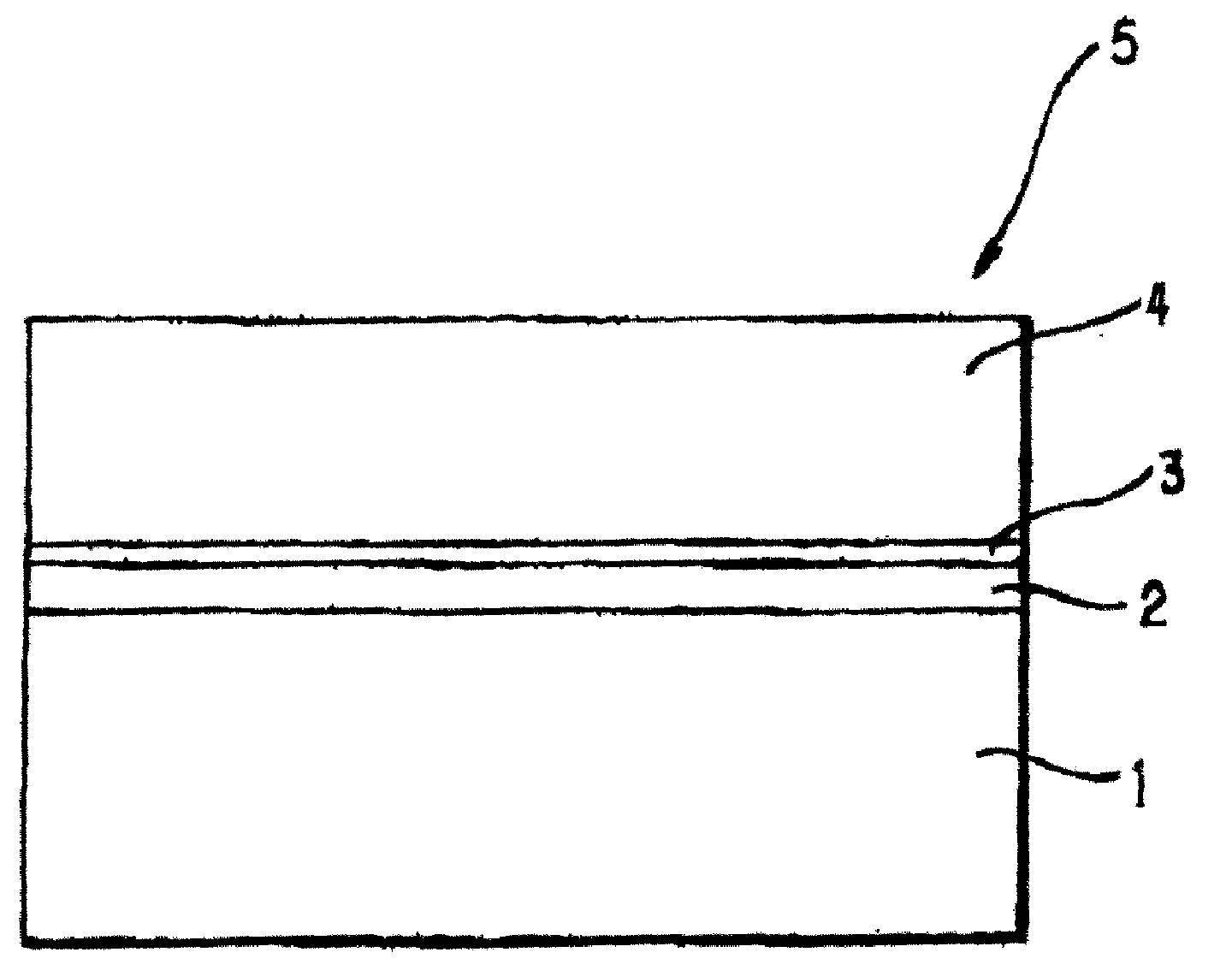
图1是一个横截面图,展示了这样得到的GaN外延层状衬底的结构。Fig. 1 is a cross-sectional view showing the structure of the GaN epitaxial layered substrate thus obtained.
特别的,图1是一个横截面图,展示了一个生长GaN外延层状衬底的实施例,衬底的生长运用了本发明的GaN晶体衬底的生长方法。In particular, FIG. 1 is a cross-sectional view showing an embodiment of growing a GaN epitaxial layered substrate, and the growth method of the GaN crystal substrate of the present invention is used for the growth of the substrate.
在这幅图里,1代表作为初始衬底的单晶蓝宝石C面衬底,2代表有C轴取向的金属膜,3代表氮化铝膜,4代表GaN膜。In this figure, 1 represents the single crystal sapphire C-plane substrate as the initial substrate, 2 represents the metal film with C-axis orientation, 3 represents the aluminum nitride film, and 4 represents the GaN film.
5代表层状衬底,将层状衬底从HVPE炉中取出后浸入由盐酸和双氧水组成的混合液中。结果,铝膜被有选择地蚀刻掉,GaN膜4就从单晶蓝宝石1的C面被分离。由于一层薄薄的AlN被附着在GaN膜4的一面(在图形的下面),这个薄层将用含有金刚石抛光粉的抛光液进行抛光而除去。最后,就得到自由固定的单晶GaN衬底。5 represents the layered substrate, and the layered substrate was taken out from the HVPE furnace and immersed in a mixed solution composed of hydrochloric acid and hydrogen peroxide. As a result, the aluminum film is selectively etched away, and the
测量了GaN单晶衬底的扭曲程度。结果,扭曲的曲率半径大概是4m,这确证这个单晶衬底的确很平。还用原子力显微镜观测了GaN单晶衬底的表面以测量表面凹陷浓度。结果,浓度低到2×10⁵pits/cm2,这确认了GaN单晶衬底有很高的结晶度。The degree of distortion of the GaN single crystal substrate was measured. As a result, the radius of curvature of the twist is about 4 m, which confirms that the single crystal substrate is indeed flat. The surface of the GaN single crystal substrate was also observed with an atomic force microscope to measure the surface pit concentration. As a result, the concentration was as low as 2×10 5 pits/cm 2 , which confirmed the high crystallinity of the GaN single crystal substrate.
(实例2)(Example 2)
将直径50.8mm(约2英寸)的单晶蓝宝石C面衬底作为初始衬底放在MOCVD炉子里面,用TMG和氨作为初始材料在600℃生长厚度为50nm的GaN膜。其后,衬底的温度被升到1050℃,然后将GaN膜生长到1μm。A single crystal sapphire C-plane substrate with a diameter of 50.8mm (about 2 inches) was placed in an MOCVD furnace as an initial substrate, and a GaN film with a thickness of 50nm was grown at 600°C with TMG and ammonia as initial materials. Thereafter, the temperature of the substrate was raised to 1050°C, and then the GaN film was grown to 1 µm.
一层0.1μm厚的金被气相沉积到这个衬底上作为金属膜,然后用X射线衍射来分析。结果,观测到金膜的(111)衍射。这确认了金膜是C轴取向的。A 0.1 μm-thick layer of gold was vapor-deposited on this substrate as a metal film, which was then analyzed by X-ray diffraction. As a result, (111) diffraction of the gold film was observed. This confirms that the gold film is C-axis oriented.
这个衬底再次被放进MOCVD炉子里面。在炉内用TMA和氨作为初始材料于衬底温度850℃时生长0.1μm厚的氮化铝膜。然后衬底温度被进一步升到1050℃,并且初始材料换成TMG和氨,然后生长厚度为2μm的GaN膜。This substrate is again placed inside the MOCVD furnace. A 0.1 μm thick AlN film was grown in a furnace using TMA and ammonia as starting materials at a substrate temperature of 850°C. Then the substrate temperature was further raised to 1050° C., and the initial materials were changed to TMG and ammonia, and then a GaN film was grown with a thickness of 2 μm.
下一步,这个衬底被转移到HVPE炉子,然后在衬底的表面沉积厚度为300μm的GaN。在这里用氨和氯化镓作为生长的初始材料。生长条件为:压力=大气压,衬底温度=1050℃,并且生长率=80μm/hr。In the next step, this substrate was transferred to a HVPE furnace, and GaN was deposited on the surface of the substrate with a thickness of 300 μm. Here ammonia and gallium chloride were used as starting materials for growth. The growth conditions were: pressure=atmospheric pressure, substrate temperature=1050°C, and growth rate=80 μm/hr.
从HVPE炉子里取出来用这种方法得到的层状衬底,再放进王水里大约一个晚上以便溶解和除去金膜,就用种方法来分开蓝宝石衬底和GaN膜。就这样就制备出了自由固定的GaN单晶衬底。用原子力显微镜观测了GaN单晶衬底表面以测量表面凹陷的浓度。结果,浓度低到4×10⁵pits/cm2,确证了GaN单晶衬底有很高的结晶度。Take out the layered substrate obtained in this way from the HVPE furnace, put it in aqua regia for about one night to dissolve and remove the gold film, and use this method to separate the sapphire substrate and the GaN film. In this way, a freely fixed GaN single crystal substrate was prepared. The surface of the GaN single crystal substrate was observed with an atomic force microscope to measure the concentration of surface pits. As a result, the concentration was as low as 4×10 5 pits/cm 2 , confirming the high crystallinity of the GaN single crystal substrate.
(实例3)(Example 3)
直径50.8mm(约2英寸)的单晶蓝宝石C面衬底作为初始衬底。运用溅射的方法,在衬底上沉积200nm厚的银作为金属膜。然后将衬底放到MOCVD炉子里面,用TMG和氨作为初始材料,在衬底温度为600℃时,于银膜的表面上生长厚度为50nm的GaN膜。然后,衬底的温度被升到1050℃,用TMG和氨作为初始材料来生长厚度为1μm的GaN膜。A single crystal sapphire C-plane substrate with a diameter of 50.8 mm (about 2 inches) was used as the initial substrate. Using the method of sputtering, 200nm thick silver is deposited on the substrate as a metal film. Then put the substrate into the MOCVD furnace, use TMG and ammonia as initial materials, and grow a GaN film with a thickness of 50nm on the surface of the silver film when the substrate temperature is 600°C. Then, the temperature of the substrate was raised to 1050° C., and a GaN film was grown to a thickness of 1 μm using TMG and ammonia as initial materials.
然后这个衬底被转移到HVPE炉子里,在衬底表面沉积厚度为300μm的GaN。在这里,氨和氯化镓被用作生长的初始材料。生长条件为:压力=大气压,衬底温度=1050℃,并且生长率=80μm/hr。This substrate was then transferred to a HVPE furnace, where GaN was deposited to a thickness of 300 μm on the substrate surface. Here, ammonia and gallium chloride were used as starting materials for growth. The growth conditions were: pressure=atmospheric pressure, substrate temperature=1050°C, and growth rate=80 μm/hr.
从HVPE炉子取出用这种方法得到的层状衬底,再浸入热硫酸以便溶解和除去银膜,就用种方法来分开蓝宝石衬底和GaN膜。就这样就制备出了自由固定的GaN单晶衬底。The layered substrate obtained in this way was taken out of the HVPE furnace, and then immersed in hot sulfuric acid to dissolve and remove the silver film, which was used to separate the sapphire substrate and the GaN film. In this way, a freely fixed GaN single crystal substrate was prepared.
用原子力显微镜观测了GaN单晶衬底表面以测量表面凹陷的浓度。结果,浓度低到9×10⁴pits/cm2,这确证了GaN单晶衬底有很高的结晶度。The surface of the GaN single crystal substrate was observed with an atomic force microscope to measure the concentration of surface pits. As a result, the concentration was as low as 9×10 4 pits/cm 2 , which confirmed the high crystallinity of the GaN single crystal substrate.
(实例4)(Example 4)
用直径50.8mm(约2英寸)的单晶蓝宝石C面衬底被作为初始衬底,以和例2同样的方式在衬底上用MOCVD方法生长厚度为1μm的单晶GaN。在这个衬底上气相沉积镍作为金属膜,然后这个被沉积过的衬底被放到MOCVD炉子里面,在炉子里,在1200℃于氢气气氛中加热衬底30分钟以便清洁表面。然后,在同一个炉子里面,于1060℃,用TMA和氨作为初始材料在衬底上生长厚度为0.1μm的AlN膜。接下来,初始材料变成了TMG和氨,在衬底上生长厚度为1μm的GaN。A single-crystal sapphire C-plane substrate with a diameter of 50.8 mm (about 2 inches) was used as the initial substrate, and a single-crystal GaN with a thickness of 1 μm was grown on the substrate by MOCVD in the same manner as in Example 2. Nickel was vapor-deposited as a metal film on the substrate, and then the deposited substrate was placed in an MOCVD furnace, where the substrate was heated at 1200°C in a hydrogen atmosphere for 30 minutes to clean the surface. Then, in the same furnace, an AlN film with a thickness of 0.1 μm was grown on the substrate at 1060° C. using TMA and ammonia as starting materials. Next, the starting materials were changed to TMG and ammonia, and GaN was grown to a thickness of 1 μm on the substrate.
这个衬底然后被转移到HVPE炉子里面,在衬底的表面沉积厚度为300μm的GaN。在这里,用氨和氯化镓作为生长的初始材料。生长条件为:压力=大气压,衬底温度=1050℃,并且生长率=80μm/hr。在生长的工艺中,引入二氯硅烷作为掺杂气体而把硅在掺杂GaN晶体里面。This substrate was then transferred into a HVPE furnace, where GaN was deposited to a thickness of 300 μm on the surface of the substrate. Here, ammonia and gallium chloride were used as starting materials for growth. The growth conditions were: pressure=atmospheric pressure, substrate temperature=1050°C, and growth rate=80 μm/hr. During the growth process, silicon is embedded in the doped GaN crystal by introducing dichlorosilane as a dopant gas.
把这样的层状衬底从HVPE炉子里取出来,再放进王水里大约一个晚上以便溶解和除去镍膜,就用种方法来分开蓝宝石衬底和GaN膜。就这样就制备出了自由固定的GaN单晶衬底。Take such a layered substrate out of the HVPE furnace, put it in aqua regia for about one night to dissolve and remove the nickel film, and use a method to separate the sapphire substrate and the GaN film. In this way, a freely fixed GaN single crystal substrate was prepared.
用保罗(Pauw)方法测量了单晶GaN膜的载流子浓度并发现是8×1018cm-3。这样就确证了制备出的是高载流子浓度的n型GaN单晶衬底。The carrier concentration of the single crystal GaN film was measured by the Pauw method and found to be 8×10 18 cm -3 . In this way, it is confirmed that the n-type GaN single crystal substrate with high carrier concentration is prepared.
用原子力显微镜观测了GaN单晶衬底表面以测量表面凹陷的浓度。结果,浓度低到6×10⁵pits/cm2,这确证了GaN单晶衬底有很高的结晶度。The surface of the GaN single crystal substrate was observed with an atomic force microscope to measure the concentration of surface pits. As a result, the concentration was as low as 6×10 5 pits/cm 2 , which confirmed the high crystallinity of the GaN single crystal substrate.
(实例5)(Example 5)
直径50.8mm(约2英寸)的单晶蓝宝石C面衬底作为初始衬底。在衬底上气相沉积厚度为0.1μm的钛作为金属膜,然后,为了防止氧化,在沉积了钛的衬底上再气相沉积厚度为10到20nm的金膜。A single crystal sapphire C-plane substrate with a diameter of 50.8 mm (about 2 inches) was used as the initial substrate. Titanium was vapor-deposited to a thickness of 0.1 [mu]m as a metal film on the substrate, and then, to prevent oxidation, a gold film was vapor-deposited to a thickness of 10 to 20 nm on the titanium-deposited substrate.
这个衬底被放进MBE炉子(分子束外延炉),于700℃在衬底上生长厚度为0.5μm的GaN膜。然后衬底被转移到HVPE炉子里面,用氨和氯化镓作为初始材料在衬底上进一步沉积厚度为300μm的GaN。生长条件为:压力=大气压,衬底温度=1050℃,并且生长率=80μm/hr。This substrate was put into an MBE furnace (Molecular Beam Epitaxy Furnace), and a GaN film was grown to a thickness of 0.5 µm on the substrate at 700°C. The substrate was then transferred into a HVPE furnace, where ammonia and gallium chloride were used as starting materials to further deposit GaN with a thickness of 300 μm on the substrate. The growth conditions were: pressure=atmospheric pressure, substrate temperature=1050°C, and growth rate=80 μm/hr.
从HVPE炉子里取出这样的层状衬底,再浸入由氢氟酸和硝酸组成的混合液中。结果,钛层被选择的蚀刻掉,GaN膜也就跟蓝宝石衬底分离开来。就这样就制备出了自由固定的GaN单晶衬底。Such layered substrates were removed from the HVPE furnace and immersed in a mixture of hydrofluoric acid and nitric acid. As a result, the titanium layer is selectively etched away and the GaN film is separated from the sapphire substrate. In this way, a freely fixed GaN single crystal substrate was prepared.
用原子力显微镜观测了GaN单晶衬底表面以测量表面凹陷的浓度。结果,浓度低到2×10⁵pits/cm2,这确证了GaN单晶衬底有很高的结晶度。The surface of the GaN single crystal substrate was observed with an atomic force microscope to measure the concentration of surface pits. As a result, the concentration was as low as 2×10 5 pits/cm 2 , which confirmed the high crystallinity of the GaN single crystal substrate.
由于在生长的工艺中引入了热应变,这种高结晶度的自由固定GaN单晶衬底有很大的扭曲,并且扭曲的曲率半径大约是70cm。这种衬底被夹在光滑的陶瓷划线台中间(未示出),并且在这种状态下1000℃退火2个小时以缓解应力。结果,扭曲的曲率半径被减小到5m。Due to the thermal strain introduced in the growth process, this highly crystalline free-fixed GaN single crystal substrate has a large twist, and the radius of curvature of the twist is about 70cm. This substrate was sandwiched between a smooth ceramic scribe table (not shown) and annealed in this state at 1000°C for 2 hours to relieve stress. As a result, the radius of curvature of the twist was reduced to 5m.
(实例6)(Example 6)
用直径50.8mm(约2英寸)的硅(111)衬底作为初始衬底,在衬底上气相沉积厚度是0.1μm的铜作为金属膜。将此衬底放进MOCD炉子里面,在氢气气氛中把衬底加热至800℃保温30分钟来清洁衬底的表面,同时也提高了取向的程度。然后,在同一个炉子里面,于800℃,用TMA和氨作为初始材料在铜的表面上生长厚度为0.1μm的AlN膜。接着,衬底的温度被升到1050℃,并且用TMG和氨作为初始材料生长厚度为1μm的GaN膜。A silicon (111) substrate with a diameter of 50.8 mm (about 2 inches) was used as an initial substrate, on which copper was vapor-deposited to a thickness of 0.1 μm as a metal film. Put the substrate into the MOCD furnace and heat the substrate to 800°C for 30 minutes in a hydrogen atmosphere to clean the surface of the substrate and improve the degree of orientation. Then, in the same furnace, an AlN film with a thickness of 0.1 µm was grown on the copper surface at 800°C using TMA and ammonia as starting materials. Next, the temperature of the substrate was raised to 1050° C., and a GaN film was grown to a thickness of 1 μm using TMG and ammonia as initial materials.
将此衬底转移到HVPE炉子里,在衬底的表面沉积300μm的GaN。在这里,用氨和氯化镓作生长的初始材料。生长条件为:压力=大气压,衬底温度=1050℃,并且生长率=80μm/hr。The substrate was transferred into a HVPE furnace, and 300 μm of GaN was deposited on the surface of the substrate. Here, ammonia and gallium chloride were used as starting materials for growth. The growth conditions were: pressure=atmospheric pressure, substrate temperature=1050°C, and growth rate=80 μm/hr.
从HVPE炉子里取出来这样的层状衬底,再浸入王水中大约一整夜以便完全溶解和去掉硅衬底和铜膜。由于一层薄薄的AlN被附着在GaN膜的一面,这个薄层会通过用含有金刚石抛光粉的抛光液进行抛光而除去。这样就制备出了自由固定的单晶GaN衬底。Such layered substrates were taken out of the HVPE furnace and immersed in aqua regia for about one night to completely dissolve and remove the silicon substrate and copper film. Since a thin layer of AlN is attached to one side of the GaN film, this thin layer is removed by polishing with a polishing solution containing diamond polishing powder. In this way, a free-fixed single-crystal GaN substrate is prepared.
用原子力显微镜观测GaN单晶衬底表面以测量表面凹陷的浓度。结果,浓度低到2×10⁴pits/cm2,这确证了GaN单晶衬底有很高的结晶度。The surface of the GaN single crystal substrate was observed with an atomic force microscope to measure the concentration of surface depressions. As a result, the concentration was as low as 2×10 4 pits/cm 2 , which confirmed the high crystallinity of the GaN single crystal substrate.
(实例7)(Example 7)
用直径50.8mm(约2英寸)的硅(111)衬底作为初始衬底,并将其放在MOCVD炉子里面,在氢气气氛中和400℃温度下,在硅表面沉积0.2μm的铝作为金属膜,同时通入TMA。然后,在同一个炉子里面,将衬底温度升到600℃,用TMG和氨作为初始的材料在铝膜的表面生长厚度为0.01μm的GaN膜。接着,将衬底温度升到1050℃,用TMG和氨作为初始材料生长厚度为2μm的GaN膜。Use a silicon (111) substrate with a diameter of 50.8 mm (about 2 inches) as the initial substrate, and place it in an MOCVD furnace, and deposit 0.2 μm of aluminum on the silicon surface as a metal in a hydrogen atmosphere at a temperature of 400 ° C membrane while passing through TMA. Then, in the same furnace, the substrate temperature was raised to 600°C, and a GaN film with a thickness of 0.01 μm was grown on the surface of the aluminum film using TMG and ammonia as initial materials. Next, the substrate temperature was raised to 1050° C., and a GaN film with a thickness of 2 μm was grown using TMG and ammonia as initial materials.
将此衬底转移到HVPE炉子里,在衬底的表面沉积300μm的GaN。在这里,用氨和氯化镓作生长的初始材料。生长条件为:压力=大气压,衬底温度=1050℃,并且生长率=80μm/hr。The substrate was transferred into a HVPE furnace, and 300 μm of GaN was deposited on the surface of the substrate. Here, ammonia and gallium chloride were used as starting materials for growth. The growth conditions were: pressure=atmospheric pressure, substrate temperature=1050°C, and growth rate=80 μm/hr.
从HVPE炉子里取出来这样的层状衬底,再浸入王水中大约一整夜以便完全溶解和去掉硅衬底和铝膜。这样就制备出了自由固定的单晶GaN衬底。Such a layered substrate was taken out of the HVPE furnace and immersed in aqua regia for about one night to completely dissolve and remove the silicon substrate and aluminum film. In this way, a free-fixed single-crystal GaN substrate is prepared.
用原子力显微镜观测GaN单晶衬底表面以测量表面凹陷的浓度。结果,浓度低到4×10⁴pits/cm2,这确证了GaN单晶衬底有很高的结晶度。The surface of the GaN single crystal substrate was observed with an atomic force microscope to measure the concentration of surface depressions. As a result, the concentration was as low as 4×10 4 pits/cm 2 , which confirmed the high crystallinity of the GaN single crystal substrate.
(实例8)(Example 8)
用直径50.8mm(约2英寸)的硅(111)衬底作为初始衬底,并将其放在MOCVD炉子里面,在氢气气氛中和400℃温度下,在硅表面沉积0.2μm的铝作为金属膜,同时通入TMA。然后,在同一个炉子里面,将衬底温度升到600℃,用TMG和氨作为初始的材料在铝膜的表面生长厚度为0.1μm的GaN膜。接着,将衬底温度升到1050℃,用TMG和氨作为初始材料生长厚度为1μm的GaN膜。Use a silicon (111) substrate with a diameter of 50.8 mm (about 2 inches) as the initial substrate, and place it in an MOCVD furnace, and deposit 0.2 μm of aluminum on the silicon surface as a metal in a hydrogen atmosphere at a temperature of 400 ° C membrane while passing through TMA. Then, in the same furnace, the substrate temperature was raised to 600°C, and a GaN film with a thickness of 0.1 μm was grown on the surface of the aluminum film using TMG and ammonia as initial materials. Next, the substrate temperature was raised to 1050° C., and a GaN film with a thickness of 1 μm was grown using TMG and ammonia as initial materials.
将此衬底转移到HVPE炉子里,在衬底的表面沉积300μm的GaN。在这里,用氨和氯化镓作生长的初始材料。生长条件为:压力=大气压,衬底温度=1050℃,并且生长率=80μm/hr。The substrate was transferred into a HVPE furnace, and 300 μm of GaN was deposited on the surface of the substrate. Here, ammonia and gallium chloride were used as starting materials for growth. The growth conditions were: pressure=atmospheric pressure, substrate temperature=1050°C, and growth rate=80 μm/hr.
从HVPE炉子里取出来这样的层状衬底,再浸入王水中大约一整夜以便完全溶解和去掉硅衬底和铝膜。这样就制备出了自由固定的单晶GaN衬底。Such a layered substrate was taken out of the HVPE furnace and immersed in aqua regia for about one night to completely dissolve and remove the silicon substrate and aluminum film. In this way, a free-fixed single-crystal GaN substrate is prepared.
用原子力显微镜观测GaN单晶衬底表面以测量表面凹陷的浓度。结果,浓度低到5×10⁴pits/cm2,这确证了GaN单晶衬底有很高的结晶度。The surface of the GaN single crystal substrate was observed with an atomic force microscope to measure the concentration of surface depressions. As a result, the concentration was as low as 5×10 4 pits/cm 2 , which confirmed the high crystallinity of the GaN single crystal substrate.
(实例9)(Example 9)
用直径50.8mm(约2英寸)的硅(111)衬底作为初始衬底,在衬底上气相沉积0.1μm厚的银作为金属膜。并将其放在MOCVD炉子里面,在氢气气氛中和650℃温度下加热30分钟来清洁衬底的表面,同时也提高了取向的程度。然后,在同一个炉子里面和650℃温度下,用TMA和氨作为初始材料在银膜表面上生长厚度为0.02μm的AlN膜。接着,将衬底温度升到1050℃,用TMA和氨作为初始材料生长厚度为0.1μm的AlN膜。再接着,初始材料换成TMG和氨,生长一层1μm厚的GaN膜。A silicon (111) substrate with a diameter of 50.8 mm (about 2 inches) was used as an initial substrate, on which silver was vapor-deposited to a thickness of 0.1 μm as a metal film. And put it in an MOCVD furnace, and heat it in a hydrogen atmosphere at a temperature of 650° C. for 30 minutes to clean the surface of the substrate, and also improve the degree of orientation. Then, in the same furnace at a temperature of 650°C, an AlN film with a thickness of 0.02 µm was grown on the surface of the silver film using TMA and ammonia as starting materials. Next, the substrate temperature was raised to 1050° C., and an AlN film with a thickness of 0.1 μm was grown using TMA and ammonia as initial materials. Then, the initial material is changed to TMG and ammonia, and a GaN film with a thickness of 1 μm is grown.
将此衬底转移到HVPE炉子里,在衬底的表面沉积400μm的GaN。在这里,用氨和氯化镓作生长的初始材料。生长条件为:压力=大气压,衬底温度=1050℃,并且生长率=80μm/hr。The substrate was transferred into a HVPE furnace, and 400 μm of GaN was deposited on the surface of the substrate. Here, ammonia and gallium chloride were used as starting materials for growth. The growth conditions were: pressure=atmospheric pressure, substrate temperature=1050°C, and growth rate=80 μm/hr.
从HVPE炉子里取出来这样的层状衬底,再浸入硝酸中大约一整夜以便完全溶解和去掉银膜。这样就制备出了自由固定的单晶GaN衬底。Such laminated substrates were taken out of the HVPE furnace and immersed in nitric acid for about one night to completely dissolve and remove the silver film. In this way, a free-fixed single-crystal GaN substrate is prepared.
用原子力显微镜观测GaN单晶衬底表面以测量表面凹陷的浓度。结果,浓度低到1×10⁵pits/cm2,这确证了GaN单晶衬底有很高的结晶度。The surface of the GaN single crystal substrate was observed with an atomic force microscope to measure the concentration of surface depressions. As a result, the concentration was as low as 1×10 5 pits/cm 2 , which confirmed the high crystallinity of the GaN single crystal substrate.
(实例10)(Example 10)
用直径50.8mm(约2英寸)表面为(111)取向的SOI衬底作为初始衬底并且放进MBE炉子里面(未示出)。在这个炉子中衬底的温度被升到了400℃,并在衬底上沉积50nm厚的一层铝作为金属膜。之后,在同一个炉子中引入等离子体裂化的氮气来氮化铝膜的表面。An SOI substrate with a diameter of 50.8 mm (approximately 2 inches) with a (111) orientation on the surface was used as a starting substrate and placed in an MBE furnace (not shown). In this furnace, the temperature of the substrate is raised to 400°C, and a 50nm thick layer of aluminum is deposited on the substrate as a metal film. Afterwards, plasma-cracked nitrogen gas was introduced in the same furnace to nitride the surface of the aluminum film.
将此衬底转移到HVPE炉子里,在衬底的表面沉积300μm的GaN。在这里,用氨和氯化镓作生长的初始材料。生长条件为:压力=大气压,衬底温度=1050℃,并且生长率=80μm/hr。The substrate was transferred into a HVPE furnace, and 300 μm of GaN was deposited on the surface of the substrate. Here, ammonia and gallium chloride were used as starting materials for growth. The growth conditions were: pressure=atmospheric pressure, substrate temperature=1050°C, and growth rate=80 μm/hr.
这样的层状衬底被浸入由氢氟酸和双氧水组成的混合液中。结果,铝膜被择优地蚀刻掉,从而GaN层和SOI衬底被分离开。测量了这样得到的GaN单晶衬底的扭曲程度。结果,衬底扭曲的曲率半径大约是4m,这确证了衬底是相当平的。Such a layered substrate is immersed in a mixture of hydrofluoric acid and hydrogen peroxide. As a result, the aluminum film is preferentially etched away, thereby separating the GaN layer and the SOI substrate. The degree of twist of the GaN single crystal substrate thus obtained was measured. As a result, the radius of curvature of the substrate twist was about 4 m, which confirmed that the substrate was quite flat.
(实例11)(Example 11)
用直径76.2mm(约3英寸)晶向为(111)的硅片作为初始衬底,通过溅射装置(未示出)在衬底上沉积0.1μm厚的铝作为金属膜。将此衬底放进HVPE炉子里面,在炉子里,这个被沉积过的衬底于600℃在氨气气氛中被加热10分钟使铝膜的表面氮化。然后,沉积GaN到350μm的厚度。在这里,用氨和氯化镓作生长的初始材料。生长条件为:压力=大气压,衬底温度=1050℃,并且生长率=80μm/hr。在生长的工艺中,二氯硅烷作为搀杂气体通入把硅掺进GaN晶体。A silicon wafer with a diameter of 76.2 mm (about 3 inches) and a crystal orientation of (111) was used as an initial substrate, and 0.1 μm thick aluminum was deposited as a metal film on the substrate by a sputtering device (not shown). The substrate was put into an HVPE furnace, and in the furnace, the deposited substrate was heated at 600°C in an ammonia atmosphere for 10 minutes to nitride the surface of the aluminum film. Then, GaN is deposited to a thickness of 350 μm. Here, ammonia and gallium chloride were used as starting materials for growth. The growth conditions were: pressure=atmospheric pressure, substrate temperature=1050°C, and growth rate=80 μm/hr. During the growth process, dichlorosilane is introduced as a dopant gas to dope silicon into the GaN crystal.
从HVPE炉子里取出来这样的层状衬底,再浸入王水中大约一整夜以便完全溶解和去掉硅衬底和铝膜。这样就制备出了自由固定的单晶GaN衬底。Such a layered substrate was taken out of the HVPE furnace and immersed in aqua regia for about one night to completely dissolve and remove the silicon substrate and aluminum film. In this way, a free-fixed single-crystal GaN substrate is prepared.
测量GaN单晶衬底的载流子浓度并发现是8×1018cm-3。这就证明制备出的是高载流子浓度的n型GaN单晶衬底。The carrier concentration of the GaN single crystal substrate was measured and found to be 8×10 18 cm -3 . This proves that the n-type GaN single crystal substrate with high carrier concentration is prepared.
(实例12)(Example 12)
用例2中描述的方法生产的直径是50.8mm(约2英寸)的单晶GaN衬底作为初始衬底,在单晶GaN衬底上,气相沉积0.1μm厚的金作为金属膜。这个沉积了金的衬底被放进MOCVD炉子里,而且在衬底温度为850℃时,用TMA和氨作为初始的材料在衬底上生长厚度为0.1μm的AlN膜。然后,衬底被加热到1050℃,并且初始材料换成TMG和氨,在衬底上生长厚度为2μm的GaN。A single-crystal GaN substrate with a diameter of 50.8 mm (about 2 inches) produced by the method described in Example 2 was used as a starting substrate, and gold was vapor-deposited to a thickness of 0.1 μm as a metal film on the single-crystal GaN substrate. The Au-deposited substrate was put into an MOCVD furnace, and an AlN film was grown on the substrate with a thickness of 0.1 μm using TMA and ammonia as initial materials at a substrate temperature of 850°C. Then, the substrate was heated to 1050° C., and the initial materials were changed to TMG and ammonia, and GaN was grown on the substrate with a thickness of 2 μm.
下一步,这个衬底被转移到HVPE炉子里面,并且在衬底上沉积厚度为300μm的GaN。在这里,用氨和氯化镓作生长的初始材料。生长条件为:压力=大气压,衬底温度=1050℃,并且生长率=80μm/hr。In the next step, this substrate is transferred into a HVPE furnace, and GaN is deposited on the substrate with a thickness of 300 μm. Here, ammonia and gallium chloride were used as starting materials for growth. The growth conditions were: pressure=atmospheric pressure, substrate temperature=1050°C, and growth rate=80 μm/hr.
从HVPE炉子里取出来这样的层状衬底,再浸入王水中大约一整夜以便完全溶解和去掉金膜。用这种方法就可以使用外延法生长的厚GaN膜和下面的GaN衬底分开。用原子力显微镜观测这样新得到的GaN单晶衬底表面来测量表面凹陷的浓度。结果,浓度为1×10⁵pits/cm2,这确证了其凹陷浓度要比下面衬底的凹陷浓度小,并且反复运用根据本发明的这种生产方法就能提供更高结晶度的GaN单晶衬底。Such layered substrates were taken out of the HVPE furnace and immersed in aqua regia for about one night to completely dissolve and remove the gold film. In this way, thick GaN films grown by epitaxy can be separated from the underlying GaN substrate. The surface of the thus newly obtained GaN single crystal substrate was observed with an atomic force microscope to measure the concentration of surface depressions. As a result, the concentration was 1×10 5 pits/cm 2 , which confirms that the pit concentration is smaller than that of the underlying substrate, and repeated application of this production method according to the present invention can provide GaN monoliths with higher crystallinity. crystal substrate.
(实例13)(Example 13)
图2是一个横截面图,表示的是另外一个GaN外延层状衬底的实施例,它运用了本发明的生产GaN晶体衬底的方法。在图1和图2中,一样的部分被标志成一样的索引数字。Fig. 2 is a cross-sectional view showing another embodiment of a GaN epitaxial layered substrate using the method for producing a GaN crystal substrate of the present invention. In Fig. 1 and Fig. 2, like parts are marked with like index numbers.
直径为50.8mm(约2英寸)的单晶蓝宝石C面衬底1被作为初始衬底,在衬底上气相沉积300nm厚的金作为金属膜2。利用热CVD方法在衬底上沉积一层SiO2膜6,通过光刻法在SiO2膜中形成平行于<11-20>的条形窗口以便露出金膜2。窗口的宽为3μm,掩模的宽为7μm。这个衬底被放进MOCVD炉子里。在这个炉子中,在衬底温度为800℃的条件下,用TMA和氨作为初始的材料在金膜2的表面上生长厚度为100nm的AlN膜3。然后,衬底温度被升到1050℃,并且用TMG和氨作为初始材料在衬底上生长厚度为1μm的GaN膜4。开始,GaN有选择的生长在窗口部分,当掩模6的窗口被GaN填满后,GaN就会在掩模上平行生长以覆盖衬底的整个表面。最后,一层平面的GaN就形成了。A single-crystal sapphire C-
将此衬底转移到HVPE炉子里面,并且在衬底的表面进一步沉积GaN直到300μm的厚度。在这里,用氨和氯化镓作生长的初始材料。生长条件为:压力=大气压,衬底温度=1050℃,并且生长率=80μm/hr。当生长完成后,在图2中所示的层状衬底7就被制备好了。This substrate was transferred inside a HVPE furnace, and GaN was further deposited on the surface of the substrate up to a thickness of 300 μm. Here, ammonia and gallium chloride were used as starting materials for growth. The growth conditions were: pressure=atmospheric pressure, substrate temperature=1050°C, and growth rate=80 μm/hr. When the growth is completed, the
从HVPE炉子里取出来这样的层状衬底7,再浸入王水中以便溶解和去掉金膜2。用这种方法就可以使GaN膜4和单晶蓝宝石C面衬底1分开。向着衬底1一面的GaN膜4被SiO2掩模6嵌入,这些SiO2掩模6用金刚石抛光粉通过机械抛光去掉。这样,就制备成了自由固定的GaN单晶衬底4。Such
运用原子力显微镜观测GaN单晶衬底4的表面来测量表面凹陷的浓度。结果,浓度低到1×10⁴pits/cm2,这确证了GaN单晶衬底有很高的结晶度。The concentration of surface depressions was measured by observing the surface of GaN
(实例14)(Example 14)
图3是一个横截面图,表示的是另外一个GaN外延层状衬底的实施例,它运用了本发明的生产GaN晶体衬底的方法。Fig. 3 is a cross-sectional view showing another embodiment of a GaN epitaxial layered substrate using the method for producing a GaN crystal substrate of the present invention.
直径为50.8mm(约2英寸)的单晶蓝宝石C面衬底1作为初始衬底,通过溅射的方法在衬底上沉积200nm厚的银膜2作为金属膜。将这个衬底放进MOCVD炉子内。在这个炉子中,在衬底温度为800℃的条件下,用TMA和氨作为初始的材料在银膜2的表面上生长厚度为150nm的AlN膜3。然后,衬底温度被升到1050℃,再用TMG和氨作为初始材料在衬底上生长厚度为1μm的GaN膜4。通过PCVD的方法在衬底上沉积0.6μm厚的一层SiO2膜6,通过光刻法在SiO2膜中形成平行于<1-100>的条形窗口以露出GaN膜。窗口的宽大约为2μm,掩模的宽为8μm。将这个衬底转移到HVPE炉子。在这个炉子里面,于衬底表面沉积300μm厚的GaN 4。在这里,用氨和氯化镓作生长的初始材料。生长条件为:压力=大气压,衬底温度=1050℃,并且生长率=80μm/hr。当生长完成后,在图3中所示的层状衬底8就被制备好了。A single crystal sapphire C-
从HVPE炉子里取出来这样的层状衬底8,再浸入热硫酸中以便溶解和去掉银膜2。用这种方法就可以使GaN膜4和单晶蓝宝石C面衬底1分开。这样,就制备出了自由固定的GaN单晶衬底4。利用原子力显微镜观测了GaN单晶衬底4的表面来测量表面凹陷的浓度。结果,浓度低到2×10⁴pits/cm2,这确证了GaN单晶衬底有很高的结晶度。Such
(实例15)(Example 15)
图4是一个横截面图,表示的是又一个GaN外延层状衬底的实施例,它运用了本发明的生产GaN晶体衬底的方法。Fig. 4 is a cross-sectional view showing still another embodiment of a GaN epitaxial layered substrate using the method for producing a GaN crystal substrate of the present invention.
通过例2中描述的方法生产的直径50.8mm(约2英寸)的单晶GaN衬底4作为初始衬底,通过热CVD方法在单晶GaN衬底4上沉积一层0.5μm厚的SiO2膜31,利用光刻法在SiO2膜31中形成平行于<1-100>的条形窗口32,以露出GaN衬底的表面。窗口32的宽大约为3μm,SiO2膜31掩模宽大约为7μm。A single crystal GaN substrate 4 with a diameter of 50.8 mm (about 2 inches) produced by the method described in Example 2 was used as an initial substrate, and a layer of 0.5 μm thick SiO was deposited on the single
将这个衬底放进MOCVD炉子内。在这个炉子中,衬底的温度被升到1050℃,用TMG和氨作为初始材料生长厚度为2μm的GaN膜33。开始,GaN有选择在窗口32上生长,当掩模的窗口被GaN填满后,GaN就会在掩模上平行生长以覆盖衬底的整个表面。最后,就形成了一层平面的GaN膜33。在衬底上气相沉积0.1μm厚的金膜34作为金属膜。然后这个沉积了金膜的衬底被放进HVPE炉子里面,接着在衬底的表面上沉积GaN 35到300μm的厚度。在这里,用氨和氯化镓作生长的初始材料。生长条件为:压力=大气压,衬底温度=1050℃,并且生长率=80μm/hr。当生长完成后,层状衬底9就被制备好了。This substrate is placed in the MOCVD furnace. In this furnace, the temperature of the substrate was raised to 1050°C, and a
从HVPE炉子里取出来这样的层状衬底9,再浸入王水里一整夜以便溶解和去掉金膜34,用这种方法就可以使用HVPE方法外延生长的GaN膜35和下面的外延GaN衬底4分开。利用原子力显微镜观测了GaN单晶衬底35的表面来测量表面凹陷的浓度。结果,浓度低到1×10⁵pits/cm2,这确证了GaN单晶衬底35有很高的结晶度。Take out such
(实例16)(Example 16)
通过在用例15中描述的生产方法制备的单晶自由固定GaN衬底35上,按照以下顺序形成一系列层制备了一个LD结构的衬底:一个硅搀杂(n=5×1017cm-3)的n型GaN缓冲层10(厚度大约2.0μm),一个硅搀杂(n=5×1017cm-3)的n型Al0.07Ga0.93N覆盖层11(厚度大约1.0μm),一个硅搀杂(n=1×1017cm-3)的n型GaN的SCH层12(厚度大约0.1μm),一个硅搀杂(或不搀杂)的In0.2Ga0.8N/In0.05Ga0.95N的多重量子阱层13(30/50×3),一个镁搀杂(p=2×1019cm-3)的p型Al0.2Ga0.91N的防过流层14(厚度大约0.02μm),一个镁搀杂(p=2×1019cm-3)的p型GaN的光限制层15(厚度大约0.1μm),一个镁搀杂(p=2×1019cm-3)的p型Al0.07Ga0.93N的覆盖层16(厚度大约0.5μm),一个镁搀杂(p=2×1019cm-3)的p型GaN的接触层17(厚度大约0.05umμm)。A substrate with an LD structure was prepared by forming a series of layers in the following order on a single-crystal free-fixed GaN substrate 35 prepared by the production method described in Example 15: a silicon-doped (n=5×10 17 cm −3 ) n-type GaN buffer layer 10 (thickness about 2.0 μm), a silicon-doped (n=5×10 17 cm -3 ) n-type Al 0.07 Ga 0.93 N cladding layer 11 (thickness about 1.0 μm), a silicon-doped (n=1×10 17 cm -3 ) n-type GaN SCH layer 12 (thickness about 0.1 μm), a silicon-doped (or undoped) In 0.2 Ga 0.8 N/In 0.05 Ga 0.95 N multiple quantum well Layer 13 (30 Å/50 Å×3), a magnesium-doped (p=2×10 19 cm -3 ) p-type Al 0.2 Ga 0.91 N overcurrent prevention layer 14 (thickness about 0.02 μm), a magnesium-doped (p=2×10 19 cm -3 ) p-type GaN optical confinement layer 15 (thickness about 0.1 μm), a Mg-doped (p=2×10 19 cm -3 ) p-type Al 0.07 Ga 0.93 N A cap layer 16 (thickness about 0.5 μm), a contact layer 17 (thickness about 0.05 μm) of p-type GaN doped with magnesium (p=2×10 19 cm −3 ).
然后,如图5所示,为了限制电流,用干法蚀刻的方法在这个有LD结构的衬底的p面上形成一个宽约为4μm深约为0.4μm的脊结构。接着,在脊上做一个镍/金电极作为p型的欧姆电极18。在这个有LD结构的衬底的自由固定GaN衬底的一侧的整个的表面上做一个钛/铝电极作为n型欧姆电极19。然后,在两个面上都做TiO2/SiO2组成的高反射覆层。该器件20的长是500μm。给该器件20加压。结果,在室温的时候,产生了持续地振动,这时的阈电流密度是4.5KA/cm2,阈电压是5.5V。此外,由于减少了晶体缺陷,当该器件20在25℃和30mW的情况下运行时,器件20的寿命将长达5000hr。尤其是,因为减小了衬底扭曲,根据本发明而采用自由固定的衬底可以实现在生产时产量的提高,并且至少80%的器件具有很好的性能。Then, as shown in FIG. 5 , in order to limit the current, a ridge structure with a width of about 4 μm and a depth of about 0.4 μm is formed on the p-plane of the substrate with the LD structure by dry etching. Next, a nickel/gold electrode is formed as a p-
图5是一个横截面的图,表示了一个光发射器件的实施例,该器件的GaN晶体衬底是根据本发明的生产方法制造的。Fig. 5 is a cross-sectional view showing an embodiment of a light-emitting device whose GaN crystal substrate is manufactured according to the production method of the present invention.
接下来,将描述最佳条件。Next, optimum conditions will be described.
在衬底上生长的金属膜的厚度最好在10-1000nm区间。这么做的原因如下。当金属膜的厚度小于10nm时,金属膜很难覆盖整个衬底的表面。在这种情况下,这会使生长在金属膜上的GaN晶体的晶核形成不均匀,结果会使GaN膜结晶度变坏。另一方面,当金属膜的厚度大于1000nm,金属膜的取向就被损坏了,这就使在金属膜上生长的GaN膜的结晶度变坏。此外,当金属膜的厚度小于10nm,衬底就不容易和GaN层分开了。The thickness of the metal film grown on the substrate is preferably in the range of 10-1000nm. The reason for this is as follows. When the thickness of the metal film is less than 10 nm, it is difficult for the metal film to cover the entire surface of the substrate. In this case, this makes the nucleation of the GaN crystal grown on the metal film uneven, with the result that the crystallinity of the GaN film deteriorates. On the other hand, when the thickness of the metal film is greater than 1000 nm, the orientation of the metal film is damaged, which deteriorates the crystallinity of the GaN film grown on the metal film. In addition, when the thickness of the metal film is less than 10nm, the substrate is not easily separated from the GaN layer.
生长在金属膜上的GaN膜的厚度不要小于50μm。这样做的原因是,当去掉了衬底之后而GaN膜被用作自由固定的衬底时,厚度小于50μm会导致缺乏机械强度,这会引起破裂也可能引起变形如扭曲。The thickness of the GaN film grown on the metal film should not be less than 50 μm. The reason for this is that when the GaN film is used as a freely fixed substrate after the substrate is removed, a thickness of less than 50 μm results in a lack of mechanical strength, which causes cracks and possibly deformation such as distortion.
在这里用金属膜作为缓冲层可以极大的减小由于衬底和GaN晶格常数及热膨胀系数的差异产生的应变。为了减小GaN的缺陷浓度,和GaN在晶格常数及热膨胀系数相近的衬底可以提供更好的结果。因此,当把本发明付诸于实践,用根据本发明生产的GaN自由固定衬底作为所要的衬底时,就可以被制备低缺陷浓度的GaN自由固定衬底。Using the metal film as the buffer layer here can greatly reduce the strain caused by the differences in lattice constant and thermal expansion coefficient between the substrate and GaN. In order to reduce the defect concentration of GaN, a substrate with a similar lattice constant and thermal expansion coefficient to GaN can provide better results. Therefore, when the present invention is put into practice and a GaN free-fixed substrate produced according to the present invention is used as a desired substrate, a GaN free-fixed substrate with a low defect concentration can be prepared.
当金属膜由铝形成时,先长在铝膜上的氮化物晶体,最好在660℃或者更低的温度下生长。当铝膜在660℃或者更高的温度下加热时,铝会融化掉,这会导致干扰取向。在这种情况下,GaN单晶膜不能在铝膜上生长。一旦氮化物晶体沉积在金属铝膜上,即便是铝膜已融化,生长在上面的GaN膜的结晶度不会被破坏掉。因为上述的这个原因,先生长金属膜上的氮化物晶体的温度最好低于这个金属的熔点。When the metal film is formed of aluminum, the nitride crystals grown on the aluminum film are preferably grown at a temperature of 660°C or lower. When the aluminum film is heated at 660° C. or higher, the aluminum melts away, which causes disturbance of orientation. In this case, a GaN single crystal film cannot be grown on an aluminum film. Once the nitride crystals are deposited on the metal aluminum film, even if the aluminum film is melted, the crystallinity of the GaN film grown on it will not be destroyed. For this reason mentioned above, the temperature at which the nitride crystal grows on the metal film is preferably lower than the melting point of the metal.
GaN膜最好通过HVPE方法来生长,因为晶体生长的速率很高,并且可以很容易的制备出一层很厚的膜。然而,其他的方法如MOCVD也可以用。此外,多种生长方法结合起来的方法也可以用。例如,可以采用以下方法:用MOCVD生长部分的GaN膜,然后用HVPE来生长GaN厚膜。GaN films are best grown by HVPE because the crystal growth rate is high and very thick films can be easily produced. However, other methods such as MOCVD can also be used. In addition, methods combining multiple growth methods can also be used. For example, a method may be employed in which a part of the GaN film is grown by MOCVD, and then a thick GaN film is grown by HVPE.
在上面的实施例中,用到了单晶蓝宝石C面衬底或者(111)硅衬底。另外,单晶碳化硅C面衬底或者多晶碳化硅C轴取向衬底也可以选用。除了Si之外,Ge、GaAs、GaP、InP或者类似物质都可以被用作单晶半导体衬底。由三元化合物的自由固定单晶衬底,如AlGaN或者GaInN,或许可以代替GaN而在金属膜上生长。这可以运用在制备镁搀杂的p型GaN衬底或类似物质。合金膜如NiAl、NiGa、CoAl、CoGa或者类似材料可以代替纯金属膜而被采用。还可以采用以下方法,就是先让有表面活性效果的元素,如硅,吸附在金属膜的表面,然后在上面生长GaN以进一步减小缺陷浓度。至于用掩模来选择性地生长,可以不用条形窗口而用,例如,圆点窗口和方格窗口来代替。还可以采用以下方法:金属膜本身具有图样,从而,GaN就会在金属膜上有选择地生长以减小GaN的缺陷浓度。In the above embodiments, a single crystal sapphire C-plane substrate or a (111) silicon substrate is used. In addition, single crystal silicon carbide C-plane substrate or polycrystalline silicon carbide C-axis orientation substrate can also be selected. Besides Si, Ge, GaAs, GaP, InP, or the like can be used as the single crystal semiconductor substrate. Free-fixed single-crystal substrates made of ternary compounds, such as AlGaN or GaInN, may be grown on metal films instead of GaN. This can be applied in the preparation of Mg-doped p-type GaN substrates or similar substances. Alloy films such as NiAl, NiGa, CoAl, CoGa, or the like can be used instead of pure metal films. The following method can also be used, that is, firstly let elements with surface active effects, such as silicon, be adsorbed on the surface of the metal film, and then grow GaN on it to further reduce the defect concentration. As for selective growth using a mask, strip windows, for example, dot windows and grid windows can be used instead. It is also possible to adopt a method in which the metal film itself has a pattern, so that GaN is selectively grown on the metal film to reduce the defect concentration of GaN.
根据本发明做的GaN晶体衬底可以被用作制备GaN器件的衬底。当根据本发明做的GaN晶体衬底作为激光二极管的衬底时,尤其如此。因为用本发明的方法可以生产低缺陷浓度的GaN晶体,所以可以制备出高度可靠的激光二极管。The GaN crystal substrate made according to the present invention can be used as a substrate for preparing GaN devices. This is especially true when a GaN crystal substrate made according to the invention is used as a substrate for a laser diode. Since GaN crystals with low defect concentration can be produced by the method of the present invention, highly reliable laser diodes can be produced.
如上所述,根据本发明,As described above, according to the present invention,
(1)因为衬底能被很容易地除去,所以可以容易地制备大尺寸和同一形状的自由固定GaN单晶衬底;(1) Since the substrate can be easily removed, a freely fixed GaN single crystal substrate of a large size and the same shape can be easily prepared;
(2)因为衬底能被很容易地除去,所以可以容易地制备没有破裂和损伤的自由固定GaN单晶衬底;(2) Since the substrate can be easily removed, a freely fixed GaN single crystal substrate without cracks and damage can be easily prepared;
(3)因为金属膜可以减小由于基体和GaN膜晶格常数和热膨胀系数差异而导致的应变,所以可以容易地制备低缺陷浓度和具有良好晶体性质的自由固定GaN单晶衬底;(3) Because the metal film can reduce the strain caused by the difference in lattice constant and thermal expansion coefficient between the substrate and the GaN film, a freely fixed GaN single crystal substrate with low defect concentration and good crystal properties can be easily prepared;
(4)自由固定的GaN单晶衬底可以运用环境友好材料及方法制备;并且(4) The freely fixed GaN single crystal substrate can be prepared using environmentally friendly materials and methods; and
(5)在低缺陷浓度和具有良好晶体性质的自由固定的GaN单晶衬底上,可以制备出高输出和长寿命的光发射器件。(5) On a freely fixed GaN single crystal substrate with low defect concentration and good crystal properties, a light-emitting device with high output and long life can be fabricated.
概述地说,本发明实现了用一个简单方式生产低缺陷浓度和没有被杂质严重污染的GaN晶体衬底的工艺,并且提供了由本工艺生产的GaN晶体衬底。In summary, the present invention realizes a process for producing a GaN crystal substrate having a low defect concentration and not being heavily contaminated with impurities in a simple manner, and provides a GaN crystal substrate produced by the process.
本发明已经参照实施例很详尽的描述过了,但是需要明白的是,变化和修改只有在本发明的范围内实行才有效,这些在以下的权利要求中有说明。The invention has been described in great detail with reference to the embodiments, but it is to be understood that changes and modifications are only effected within the scope of the invention, which are specified in the following claims.
Claims (40)
Applications Claiming Priority (2)
| Application Number | Priority Date | Filing Date | Title |
|---|---|---|---|
| JP2001088294 | 2001-03-26 | ||
| JP2001088294A JP2002284600A (en) | 2001-03-26 | 2001-03-26 | Gallium nitride crystal substrate manufacturing method and gallium nitride crystal substrate |
Publications (2)
| Publication Number | Publication Date |
|---|---|
| CN1378238A CN1378238A (en) | 2002-11-06 |
| CN1249780C true CN1249780C (en) | 2006-04-05 |
Family
ID=18943411
Family Applications (1)
| Application Number | Title | Priority Date | Filing Date |
|---|---|---|---|
| CNB021078866A Expired - Fee Related CN1249780C (en) | 2001-03-26 | 2002-03-26 | Method for growing GaN crystal chip and GaN crystal chip |
Country Status (6)
| Country | Link |
|---|---|
| US (1) | US6824610B2 (en) |
| EP (1) | EP1245702A3 (en) |
| JP (1) | JP2002284600A (en) |
| KR (1) | KR100838433B1 (en) |
| CN (1) | CN1249780C (en) |
| TW (1) | TW538548B (en) |
Cited By (1)
| Publication number | Priority date | Publication date | Assignee | Title |
|---|---|---|---|---|
| CN103996607A (en) * | 2014-05-30 | 2014-08-20 | 广州市众拓光电科技有限公司 | Metal Al monocrystal film growing on sapphire substrate and preparing method and application of metal Al monocrystal film |
Families Citing this family (63)
| Publication number | Priority date | Publication date | Assignee | Title |
|---|---|---|---|---|
| JP3631724B2 (en) * | 2001-03-27 | 2005-03-23 | 日本電気株式会社 | Group III nitride semiconductor substrate and manufacturing method thereof |
| JP2004107114A (en) * | 2002-09-17 | 2004-04-08 | Toyoda Gosei Co Ltd | Method of manufacturing group iii nitride compound semiconductor substrate |
| JP4545389B2 (en) * | 2003-03-26 | 2010-09-15 | 日本碍子株式会社 | Dislocation reduction method for epitaxial substrate and group III nitride layer group |
| FR2852974A1 (en) * | 2003-03-31 | 2004-10-01 | Soitec Silicon On Insulator | PROCESS FOR THE PRODUCTION OF MONOCRYSTALLINE CRYSTALS |
| US6825123B2 (en) * | 2003-04-15 | 2004-11-30 | Saint-Goban Ceramics & Plastics, Inc. | Method for treating semiconductor processing components and components formed thereby |
| JP4457576B2 (en) | 2003-05-08 | 2010-04-28 | 住友電気工業株式会社 | Group III-V compound crystal and method for producing the same |
| JP4390640B2 (en) * | 2003-07-31 | 2009-12-24 | シャープ株式会社 | Nitride semiconductor laser device, nitride semiconductor light emitting device, nitride semiconductor wafer, and methods of manufacturing the same |
| CN100453712C (en) * | 2003-08-28 | 2009-01-21 | 日立电线株式会社 | III-V nitride-based semiconductor substrate and manufacturing method thereof |
| FR2860248B1 (en) | 2003-09-26 | 2006-02-17 | Centre Nat Rech Scient | PROCESS FOR PRODUCING AUTOMATED SUBSTRATES OF ELEMENT III NITRIDES BY HETERO-EPITAXIA ON A SACRIFICIAL LAYER |
| CN101661910B (en) * | 2003-10-27 | 2012-07-18 | 住友电气工业株式会社 | Gallium nitride semiconductor substrate and blue luminescent device |
| TWI234298B (en) * | 2003-11-18 | 2005-06-11 | Itswell Co Ltd | Semiconductor light emitting diode and method for manufacturing the same |
| KR100613273B1 (en) * | 2003-12-30 | 2006-08-18 | 주식회사 이츠웰 | Light emitting diodes and manufacturing method thereof |
| KR101094403B1 (en) * | 2004-01-29 | 2011-12-15 | 삼성코닝정밀소재 주식회사 | Reduced warpage of sapphire / gallium nitride laminates |
| WO2005074048A1 (en) * | 2004-01-31 | 2005-08-11 | Itswell Co. Ltd. | Free-standing semiconductor substrate and the manufacturing method and manufacturing apparatus thereof |
| US8174037B2 (en) * | 2004-09-22 | 2012-05-08 | Cree, Inc. | High efficiency group III nitride LED with lenticular surface |
| KR100728533B1 (en) * | 2004-11-23 | 2007-06-15 | 삼성코닝 주식회사 | Gallium nitride single crystal thick film and method for manufacturing same |
| EP1681712A1 (en) | 2005-01-13 | 2006-07-19 | S.O.I. Tec Silicon on Insulator Technologies S.A. | Method of producing substrates for optoelectronic applications |
| DE102005003884A1 (en) * | 2005-01-24 | 2006-08-03 | Forschungsverbund Berlin E.V. | Process for the preparation of c-plane oriented GaN or AlxGa1-xN substrates |
| JP4817673B2 (en) * | 2005-02-25 | 2011-11-16 | 三洋電機株式会社 | Nitride semiconductor device fabrication method |
| KR100976268B1 (en) | 2005-04-04 | 2010-08-18 | 가부시키가이샤 토호쿠 테크노 아치 | BAN single crystal growth method, BAN substrate fabrication method, BAN device manufacturing method and BAN device |
| GB0509328D0 (en) * | 2005-05-09 | 2005-06-15 | Univ Nottingham | A bulk, free-standing cubic III-N substrate and a method for forming same |
| CN100561669C (en) * | 2005-05-16 | 2009-11-18 | 中国科学院合肥物质科学研究院 | Preparation method of gallium nitride thin film material |
| KR20060131327A (en) * | 2005-06-16 | 2006-12-20 | 엘지전자 주식회사 | Manufacturing method of light emitting diode |
| KR100638869B1 (en) * | 2005-06-21 | 2006-10-27 | 삼성전기주식회사 | A method of forming a nitride compound layer and a method of manufacturing a BAN substrate and a vertical structure nitride semiconductor light emitting device using the same |
| CN100338790C (en) * | 2005-09-30 | 2007-09-19 | 晶能光电(江西)有限公司 | Method for preparing InGaAlN thin film on silicon bulk |
| JP2007134388A (en) * | 2005-11-08 | 2007-05-31 | Sharp Corp | Nitride-based semiconductor device and manufacturing method thereof |
| US20090081109A1 (en) * | 2005-11-17 | 2009-03-26 | Mosaic Crystals Ltd. | GaN CRYSTAL SHEET |
| JP5131889B2 (en) * | 2005-12-06 | 2013-01-30 | 学校法人 名城大学 | Method of manufacturing nitride compound semiconductor device |
| US7897490B2 (en) * | 2005-12-12 | 2011-03-01 | Kyma Technologies, Inc. | Single crystal group III nitride articles and method of producing same by HVPE method incorporating a polycrystalline layer for yield enhancement |
| WO2007072984A1 (en) * | 2005-12-20 | 2007-06-28 | Tohoku Techno Arch Co., Ltd. | Semiconductor substrate manufacturing method and element structure manufacturing method |
| US9406505B2 (en) * | 2006-02-23 | 2016-08-02 | Allos Semiconductors Gmbh | Nitride semiconductor component and process for its production |
| KR100813561B1 (en) * | 2006-03-14 | 2008-03-17 | 주식회사 이츠웰 | Semiconductor substrate and manufacturing method thereof |
| JP4860309B2 (en) * | 2006-03-17 | 2012-01-25 | 日本碍子株式会社 | Group III nitride crystal manufacturing apparatus and group III nitride crystal multilayer structure manufacturing method |
| JP5287240B2 (en) | 2006-03-29 | 2013-09-11 | 富士通株式会社 | Method for manufacturing compound semiconductor wafer having polycrystalline SiC substrate |
| WO2007114033A1 (en) * | 2006-03-31 | 2007-10-11 | Shin-Etsu Handotai Co., Ltd. | Method for manufacturing light emitting element, compound semiconductor wafer, and light emitting element |
| JP4997502B2 (en) * | 2006-09-20 | 2012-08-08 | 国立大学法人東北大学 | Manufacturing method of semiconductor device |
| JP4852755B2 (en) * | 2006-09-20 | 2012-01-11 | 国立大学法人東北大学 | Method for manufacturing compound semiconductor device |
| KR100843474B1 (en) * | 2006-12-21 | 2008-07-03 | 삼성전기주식회사 | Group III nitride single crystal growth method and nitride single crystal prepared using the same |
| CN101221898B (en) * | 2007-01-08 | 2011-05-11 | 晶能光电(江西)有限公司 | Method for manufacturing metallic substrate with high quality surface |
| US7749325B2 (en) | 2007-01-22 | 2010-07-06 | Sumitomo Electric Industries, Ltd. | Method of producing gallium nitride (GaN) independent substrate, method of producing GaN crystal body, and method of producing GaN substrate |
| JP4877241B2 (en) * | 2008-02-01 | 2012-02-15 | 豊田合成株式会社 | Method for producing group III nitride compound semiconductor substrate |
| JP5014217B2 (en) * | 2008-03-18 | 2012-08-29 | Dowaエレクトロニクス株式会社 | Group III nitride semiconductor and method of manufacturing the same |
| JP5075692B2 (en) * | 2008-03-18 | 2012-11-21 | 古河機械金属株式会社 | Group III nitride semiconductor substrate forming substrate |
| JP4809471B2 (en) * | 2008-12-26 | 2011-11-09 | Dowaホールディングス株式会社 | Group III nitride semiconductor growth substrate, group III nitride semiconductor epitaxial substrate, group III nitride semiconductor device, group III nitride semiconductor free-standing substrate, and methods of manufacturing the same |
| JP5684551B2 (en) * | 2008-12-26 | 2015-03-11 | Dowaホールディングス株式会社 | Group III nitride semiconductor growth substrate, group III nitride semiconductor epitaxial substrate, group III nitride semiconductor device, group III nitride semiconductor free-standing substrate, and methods of manufacturing the same |
| JP5576409B2 (en) | 2009-03-13 | 2014-08-20 | サン−ゴバン セラミックス アンド プラスティクス,インコーポレイティド | Chemical mechanical planarization using nanodiamonds |
| CN102804408B (en) * | 2009-09-10 | 2016-01-20 | 密歇根大学董事会 | Method for fabricating flexible photovoltaic devices using epitaxial lift-off and maintaining the integrity of growth substrates used in epitaxial growth |
| JP5515770B2 (en) * | 2009-09-14 | 2014-06-11 | 住友電気工業株式会社 | Method of forming nitride semiconductor epitaxial layer and method of manufacturing nitride semiconductor device |
| DE102010027411A1 (en) * | 2010-07-15 | 2012-01-19 | Osram Opto Semiconductors Gmbh | Semiconductor component, substrate and method for producing a semiconductor layer sequence |
| JP5741042B2 (en) * | 2011-02-14 | 2015-07-01 | 富士通株式会社 | Compound semiconductor device and manufacturing method thereof |
| US9312436B2 (en) | 2011-05-16 | 2016-04-12 | Kabushiki Kaisha Toshiba | Nitride semiconductor device, nitride semiconductor wafer, and method for manufacturing nitride semiconductor layer |
| US20120292648A1 (en) * | 2011-05-16 | 2012-11-22 | Kabushiki Kaisha Toshiba | Nitride semiconductor device, nitride semiconductor wafer, and method for manufacturing nitride semiconductor layer |
| JP5551131B2 (en) * | 2011-09-14 | 2014-07-16 | 株式会社東芝 | Manufacturing method of nitride semiconductor multilayer structure |
| US9236271B2 (en) * | 2012-04-18 | 2016-01-12 | Globalfoundries Inc. | Laser-initiated exfoliation of group III-nitride films and applications for layer transfer and patterning |
| KR20140019366A (en) * | 2012-05-23 | 2014-02-14 | 엔지케이 인슐레이터 엘티디 | Composite substrates, light emitting devices and a method of producing composite substrates |
| US9252324B2 (en) | 2013-05-30 | 2016-02-02 | Globalfoundries Inc | Heterojunction light emitting diode |
| US10241398B2 (en) * | 2015-05-21 | 2019-03-26 | Ev Group E. Thallner Gmbh | Method for application of an overgrowth layer on a germ layer |
| JP6947827B2 (en) | 2016-09-23 | 2021-10-13 | サン−ゴバン セラミックス アンド プラスティクス,インコーポレイティドSaint−Gobain Ceramics And Plastics, Inc. | Chemically mechanically flattened slurry and its formation method |
| KR102742153B1 (en) * | 2016-10-21 | 2024-12-12 | 삼성전자주식회사 | Methods of manufacturing a gallium nitride substrate |
| KR102849602B1 (en) * | 2019-09-30 | 2025-08-21 | 가부시키가이샤 플로스피아 | Laminated structures and semiconductor devices |
| FR3112238A1 (en) | 2020-07-06 | 2022-01-07 | Saint-Gobain Lumilog | SEMICONDUCTOR SUBSTRATE WITH NITRURED INTERFACE LAYER |
| CN113078046B (en) * | 2021-03-26 | 2022-07-29 | 华厦半导体(深圳)有限公司 | Gallium nitride homogeneous substrate and preparation method thereof |
| CN114059036B (en) * | 2021-11-23 | 2023-03-14 | 南京大学 | Application of iron film in auxiliary stripping of diamond polycrystalline film |
Family Cites Families (9)
| Publication number | Priority date | Publication date | Assignee | Title |
|---|---|---|---|---|
| JPS63188983A (en) | 1987-01-31 | 1988-08-04 | Ricoh Co Ltd | semiconductor light emitting device |
| JP3139445B2 (en) | 1997-03-13 | 2001-02-26 | 日本電気株式会社 | GaN-based semiconductor growth method and GaN-based semiconductor film |
| JP3788037B2 (en) | 1998-06-18 | 2006-06-21 | 住友電気工業株式会社 | GaN single crystal substrate |
| US6218280B1 (en) * | 1998-06-18 | 2001-04-17 | University Of Florida | Method and apparatus for producing group-III nitrides |
| GB9916549D0 (en) * | 1999-07-14 | 1999-09-15 | Arima Optoelectronics Corp | Epitaxial growth method of semiconductors on highly lattice mismatched substrates using the buffer layer with solid-liquid phase transition |
| US6563144B2 (en) * | 1999-09-01 | 2003-05-13 | The Regents Of The University Of California | Process for growing epitaxial gallium nitride and composite wafers |
| WO2002013245A1 (en) * | 2000-08-04 | 2002-02-14 | The Regents Of The University Of California | Method of controlling stress in gallium nitride films deposited on substrates |
| US6649494B2 (en) * | 2001-01-29 | 2003-11-18 | Matsushita Electric Industrial Co., Ltd. | Manufacturing method of compound semiconductor wafer |
| US6589857B2 (en) * | 2001-03-23 | 2003-07-08 | Matsushita Electric Industrial Co., Ltd. | Manufacturing method of semiconductor film |
-
2001
- 2001-03-26 JP JP2001088294A patent/JP2002284600A/en active Pending
-
2002
- 2002-03-26 EP EP02252184A patent/EP1245702A3/en not_active Withdrawn
- 2002-03-26 CN CNB021078866A patent/CN1249780C/en not_active Expired - Fee Related
- 2002-03-26 TW TW091105958A patent/TW538548B/en not_active IP Right Cessation
- 2002-03-26 US US10/106,693 patent/US6824610B2/en not_active Expired - Lifetime
- 2002-03-26 KR KR1020020016387A patent/KR100838433B1/en not_active Expired - Fee Related
Cited By (2)
| Publication number | Priority date | Publication date | Assignee | Title |
|---|---|---|---|---|
| CN103996607A (en) * | 2014-05-30 | 2014-08-20 | 广州市众拓光电科技有限公司 | Metal Al monocrystal film growing on sapphire substrate and preparing method and application of metal Al monocrystal film |
| CN103996607B (en) * | 2014-05-30 | 2016-10-19 | 广州市众拓光电科技有限公司 | Growth metal Al monocrystal thin films on a sapphire substrate and its preparation method and application |
Also Published As
| Publication number | Publication date |
|---|---|
| TW538548B (en) | 2003-06-21 |
| US20020175340A1 (en) | 2002-11-28 |
| KR20020076167A (en) | 2002-10-09 |
| KR100838433B1 (en) | 2008-06-16 |
| EP1245702A3 (en) | 2005-06-29 |
| US6824610B2 (en) | 2004-11-30 |
| EP1245702A2 (en) | 2002-10-02 |
| CN1378238A (en) | 2002-11-06 |
| JP2002284600A (en) | 2002-10-03 |
Similar Documents
| Publication | Publication Date | Title |
|---|---|---|
| CN1249780C (en) | Method for growing GaN crystal chip and GaN crystal chip | |
| CN1219314C (en) | Semiconductor substrate made of group III nitride and its manufacturing process | |
| CN1259734C (en) | Nitride semiconductor, manufacturing method thereof, and nitride semiconductor device | |
| CN1196176C (en) | GaN monocrystal substrate and making method thereof | |
| CN1269999C (en) | Method for doping oxygen to gallium nitride crystal and oxygen-doped n-type gallium nitride single crystal substrate | |
| CN100344004C (en) | GaN single crystal substrate and method of making the same | |
| CN1268046C (en) | Method for forming group III nitride semiconductor layer and semiconductor device | |
| CN1666319A (en) | Group III nitride semiconductor substrate and its production process | |
| TWI479541B (en) | A group III nitride semiconductor semiconductor substrate, a group III nitride semiconductor device, and a group III nitride semiconductor device, and a group III nitride semiconductor self-supporting substrate, and a method of manufacturing the same | |
| CN101060102B (en) | Nitride semiconductor substrate, manufacturing method thereof, and epitaxial substrate for nitride semiconductor light-emitting device | |
| CN1734247A (en) | Group III-V nitride-based semiconductor substrate, manufacturing method thereof, and Group III-V nitride-based semiconductor | |
| CN1882720A (en) | Method of producing self-supporting substrates comprising iii-nitrides by means of heteroepitaxy on a sacrificial layer | |
| CN1670918A (en) | Method for preparing single crystal GaN substrate and single crystal GaN substrate | |
| CN1698213A (en) | Semiconductor light-emitting element and method for manufacturing same, integrated semiconductor light-emitting device and method for manufacturing same, image display and method for manufacturing sam | |
| CN1518138A (en) | Method of fabricating a group III nitride substrate | |
| CN1960014A (en) | Nitride-based semiconductor substrate and method of making the same | |
| CN1303131A (en) | Basis substrate for crystal growth and method for making substrate using same | |
| JP4862442B2 (en) | Method for manufacturing group III-V nitride semiconductor substrate and method for manufacturing group III-V nitride device | |
| CN1639393A (en) | Group III nitride semiconductor crystal, production method thereof and group III nitride semiconductor epitaxial wafer | |
| CN1918717A (en) | Compound semiconductor multilayer structure based on gallium nitride and its manufacturing method | |
| CN100341115C (en) | Method for producing group III nitride semiconductor crystal, method for producing gallium nitride-based compound semiconductor, gallium nitride-based compound semiconductor, gallium nitride-based compound semiconductor light-emitting device, and light source using semiconductor light-emitting device | |
| CN101061571A (en) | Semiconductor multilayer substrate, manufacturing method thereof, and light emitting element | |
| CN1914743A (en) | Gallium nitride-based compound semiconductor multilayer structure and production method thereof | |
| CN1744301A (en) | Sapphire substrate, epitaxial substrate and semiconductor device | |
| CN1910738A (en) | Group III nitride semiconductor multilayer structure |
Legal Events
| Date | Code | Title | Description |
|---|---|---|---|
| C06 | Publication | ||
| PB01 | Publication | ||
| C10 | Entry into substantive examination | ||
| SE01 | Entry into force of request for substantive examination | ||
| C14 | Grant of patent or utility model | ||
| GR01 | Patent grant | ||
| ASS | Succession or assignment of patent right |
Owner name: HITACHI METALS, LTD. Free format text: FORMER OWNER: HITACHI CABLE CO., LTD. Effective date: 20150121 |
|
| C41 | Transfer of patent application or patent right or utility model | ||
| TR01 | Transfer of patent right |
Effective date of registration: 20150121 Address after: Tokyo, Japan Patentee after: HITACHI METALS, Ltd. Patentee after: NEC Corp. Address before: Tokyo, Japan Patentee before: Hitachi Cable Co.,Ltd. Patentee before: NEC Corp. |
|
| ASS | Succession or assignment of patent right |
Owner name: SCIOCS COMPANY LIMITED OCS Free format text: FORMER OWNER: HITACHI METALS, LTD. Effective date: 20150907 |
|
| C41 | Transfer of patent application or patent right or utility model | ||
| TR01 | Transfer of patent right |
Effective date of registration: 20150907 Address after: Ibaraki, Japan Patentee after: Syokusi Patentee after: NEC Corp. Address before: Tokyo, Japan Patentee before: HITACHI METALS, Ltd. Patentee before: NEC Corp. |
|
| C41 | Transfer of patent application or patent right or utility model | ||
| TR01 | Transfer of patent right |
Effective date of registration: 20160317 Address after: Tokyo, Japan Patentee after: SUMITOMO CHEMICAL Co.,Ltd. Address before: Ibaraki, Japan Patentee before: Syokusi Effective date of registration: 20160317 Address after: Ibaraki, Japan Patentee after: Syokusi Address before: Ibaraki, Japan Patentee before: Syokusi Patentee before: NEC Corp. |
|
| CF01 | Termination of patent right due to non-payment of annual fee | ||
| CF01 | Termination of patent right due to non-payment of annual fee |
Granted publication date: 20060405 Termination date: 20200326 |