CN1286830A - Tuning bandwidth minimization for low voltage dual band receiver - Google Patents
Tuning bandwidth minimization for low voltage dual band receiver Download PDFInfo
- Publication number
- CN1286830A CN1286830A CN 98813194 CN98813194A CN1286830A CN 1286830 A CN1286830 A CN 1286830A CN 98813194 CN98813194 CN 98813194 CN 98813194 A CN98813194 A CN 98813194A CN 1286830 A CN1286830 A CN 1286830A
- Authority
- CN
- China
- Prior art keywords
- frequency
- band
- signal
- oscillator
- frequency range
- Prior art date
- Legal status (The legal status is an assumption and is not a legal conclusion. Google has not performed a legal analysis and makes no representation as to the accuracy of the status listed.)
- Pending
Links
Images


Classifications
-
- H—ELECTRICITY
- H04—ELECTRIC COMMUNICATION TECHNIQUE
- H04B—TRANSMISSION
- H04B1/00—Details of transmission systems, not covered by a single one of groups H04B3/00 - H04B13/00; Details of transmission systems not characterised by the medium used for transmission
- H04B1/005—Details of transmission systems, not covered by a single one of groups H04B3/00 - H04B13/00; Details of transmission systems not characterised by the medium used for transmission adapting radio receivers, transmitters andtransceivers for operation on two or more bands, i.e. frequency ranges
- H04B1/0053—Details of transmission systems, not covered by a single one of groups H04B3/00 - H04B13/00; Details of transmission systems not characterised by the medium used for transmission adapting radio receivers, transmitters andtransceivers for operation on two or more bands, i.e. frequency ranges with common antenna for more than one band
- H04B1/0057—Details of transmission systems, not covered by a single one of groups H04B3/00 - H04B13/00; Details of transmission systems not characterised by the medium used for transmission adapting radio receivers, transmitters andtransceivers for operation on two or more bands, i.e. frequency ranges with common antenna for more than one band using diplexing or multiplexing filters for selecting the desired band
-
- H—ELECTRICITY
- H03—ELECTRONIC CIRCUITRY
- H03D—DEMODULATION OR TRANSFERENCE OF MODULATION FROM ONE CARRIER TO ANOTHER
- H03D7/00—Transference of modulation from one carrier to another, e.g. frequency-changing
- H03D7/16—Multiple-frequency-changing
- H03D7/161—Multiple-frequency-changing all the frequency changers being connected in cascade
- H03D7/163—Multiple-frequency-changing all the frequency changers being connected in cascade the local oscillations of at least two of the frequency changers being derived from a single oscillator
-
- H—ELECTRICITY
- H04—ELECTRIC COMMUNICATION TECHNIQUE
- H04B—TRANSMISSION
- H04B1/00—Details of transmission systems, not covered by a single one of groups H04B3/00 - H04B13/00; Details of transmission systems not characterised by the medium used for transmission
- H04B1/005—Details of transmission systems, not covered by a single one of groups H04B3/00 - H04B13/00; Details of transmission systems not characterised by the medium used for transmission adapting radio receivers, transmitters andtransceivers for operation on two or more bands, i.e. frequency ranges
- H04B1/0053—Details of transmission systems, not covered by a single one of groups H04B3/00 - H04B13/00; Details of transmission systems not characterised by the medium used for transmission adapting radio receivers, transmitters andtransceivers for operation on two or more bands, i.e. frequency ranges with common antenna for more than one band
- H04B1/006—Details of transmission systems, not covered by a single one of groups H04B3/00 - H04B13/00; Details of transmission systems not characterised by the medium used for transmission adapting radio receivers, transmitters andtransceivers for operation on two or more bands, i.e. frequency ranges with common antenna for more than one band using switches for selecting the desired band
Landscapes
- Engineering & Computer Science (AREA)
- Computer Networks & Wireless Communication (AREA)
- Signal Processing (AREA)
- Power Engineering (AREA)
- Stabilization Of Oscillater, Synchronisation, Frequency Synthesizers (AREA)
- Superheterodyne Receivers (AREA)
Abstract
移动无线电话根据在每个频带的最高和最低预期的接收频率处对中频进行限制,从而得到最小化的调谐带宽。可以构建双频段、双模式移动电话,它使用较少的电池单元在不用附加电路的情况下保持或改进交调性能。
Mobile wireless phones limit the intermediate frequency (IF) based on the highest and lowest expected receive frequencies in each band, thereby minimizing the tuning bandwidth. Dual-band, dual-mode mobile phones can be built that maintain or improve intermodulation performance using fewer battery cells without additional circuitry.
Description
本申请是1997年11月19日提交的专利申请序列号08/974,227的部分继续申请。This application is a continuation-in-part of patent application Serial No. 08/974,227 filed November 19,1997.
发明领域field of invention
本发明涉及使用一对选择的发送和接收频率的移动通信,以及涉及主VCO振荡器的调谐带宽的最小化。The present invention relates to mobile communications using a pair of selected transmit and receive frequencies, and to minimization of the tuning bandwidth of the main VCO oscillator.
发明背景Background of the invention
众所周知,在移动无线电话技术中,采用接收机来接收一个接收频率信号,而发射机同时在另一个方向上发送一个发送频率信号,发送频率与接收频率相隔一个被称为双工间隔的恒定偏差。As is well known in mobile radiotelephony, a receiver is used to receive a signal at a receive frequency while a transmitter simultaneously transmits in the other direction a signal at a transmit frequency separated by a constant offset called the duplex separation .
虽然双工间隔通常是一个常量,但它可以是取决于移动电话正在运行的频段的不同常量。这样,在构建运行在一个以上的频段的移动电话时会带来复杂性。While the duplex interval is usually a constant, it can be a different constant depending on the frequency band the mobile phone is operating on. This introduces complications when building a mobile phone that operates in more than one frequency band.
题目为“Transmit Signal Generation with the Aid ofReceiver(借助于接收机产生发送信号)”(Dolman)的美国专利申请序列号No.08/795,930描述了使用接收机的第二本地振荡器作为参考频率,通过该参考频率,相对于接收频率来进行发送频率控制,以便达到第一或第二双工间隔。Dolman的专利申请在此引用,以供参考。U.S. Patent Application Serial No. 08/795,930, entitled "Transmit Signal Generation with the Aid of Receiver" (Dolman), describes the use of the receiver's second local oscillator as a reference frequency by The reference frequency is used to control the transmission frequency relative to the reception frequency so as to achieve the first or second duplex interval. Dolman's patent application is hereby incorporated by reference.
从现有技术中也获知,当把两个频率综合器PLL电路封装在一个共同的集成电路中时,可将两个PLL的参考分频器进行同步或互相联系,以使得它们的相位比较器不会互相干扰。市面上有售的Philips公司的UM1005和8026双综合器集成电路采用了这种技术。这些电路包括使用分数-N分频器和可编程环路带宽,例如在美国专利No.5,095,288和5,180,993中所描述的那样,这些专利在此引用,以供参考。在美国专利No.5,535,432和5,610,559中所描述了在双模式卫星/蜂窝电话中采用这样的综合器的新颖方式,以便达到不同频段中的不同的调谐步长,这些专利也在此引用,以供参考。It is also known from the prior art that when two frequency synthesizer PLL circuits are packaged in a common integrated circuit, the reference dividers of the two PLLs can be synchronized or interconnected so that their phase comparators will not interfere with each other. This technique is used in the UM1005 and 8026 dual-synthesizer integrated circuits of Philips, which are available in the market. These circuits include the use of fractional-N dividers and programmable loop bandwidths, such as those described in US Patent Nos. 5,095,288 and 5,180,993, which are incorporated herein by reference. Novel ways of employing such synthesizers in dual-mode satellite/cellular telephones to achieve different tuning steps in different frequency bands are described in U.S. Patent Nos. 5,535,432 and 5,610,559, which patents are also incorporated herein by reference. refer to.
电子学中的不断进步便于创造符合各种各样的国内和国际协议的更小的移动电话。作为在欧洲被称为GSM、和在美国被称为PCS 1900的国际移动电话标准,其运行时的发送/接收双工间隔,对于欧洲900MHz频段是45MHz,对于欧洲1800MHz频段是95MHz,以及对于美国1900MHz PCS频段是80MHz。信道间隔是200kHz(13MHz/65),以及发送符号速率是13MHz/48。在该标准中的所有定时都涉及13MHz时钟,正如所公知的那样。在被称为DAMPS的美国IS 136系统中,运行时的双工间隔在US 800MHz蜂窝频段是45MHz,以及在US 1900MHzPCS频段是80.4MHz,调谐步长为30kHz和发送符号速率为24.3千符号/秒。在IS 136中,正如所公知的,调谐步长、符号速率和内部定时都是可从19.44MHz时钟得到的。另一个被称为IS 95的美国标准使用以1228.8MHz的发送码片速率的码分多址,在800MHz频段,以45MHz的双工间隔结合30kHz的调谐步长,以及在1900MHz频段,是50kHz步长结合80MHz的双工间隔。在IS 95中,码片速率和频率步长不容易从同一个晶体振荡器得到。可能很容易看到,如果要在同一个手持单元中组合两个或多个上述的协议,则会由于各种各样的必须对调谐步长、双工间隔、和符号速率进行同步的要求而受阻。因此,需要一种改进的射频结构,以使得这样的组合易于实行。Continuous advances in electronics have facilitated the creation of smaller mobile phones that conform to a wide variety of domestic and international protocols. As an international mobile telephony standard known as GSM in Europe and PCS 1900 in the US, it operates with a transmit/receive duplex spacing of 45MHz for the European 900MHz band, 95MHz for the European 1800MHz band, and 45MHz for the US The 1900MHz PCS frequency band is 80MHz. The channel spacing is 200kHz (13MHz/65), and the transmitted symbol rate is 13MHz/48. All timing in this standard refers to a 13 MHz clock, as is known. In the US IS 136 system known as DAMPS, the operating duplex spacing is 45MHz in the US 800MHz cellular band and 80.4MHz in the US 1900MHz PCS band, with a tuning step size of 30kHz and a transmitted symbol rate of 24.3 ksymbols/second . In IS 136, tuning step size, symbol rate and internal timing are all available from a 19.44 MHz clock as is known. Another US standard known as IS 95 uses code division multiple access at a transmit chip rate of 1228.8MHz, with a duplex spacing of 45MHz in combination with tuning steps of 30kHz on the 800MHz band and 50kHz steps on the 1900MHz band. Long combined with a duplex spacing of 80MHz. In IS 95, chip rate and frequency step size are not easily obtained from the same crystal oscillator. It may be easy to see that if two or more of the above-mentioned protocols were to be combined in the same handheld unit, there would be limitations due to the various requirements that must be synchronized for tuning step size, duplex spacing, and symbol rate. stymied. Therefore, there is a need for an improved radio frequency structure to make such a combination easy to implement.
因为移动电话被设计成采用更少的电池单元,对于接收机中的适当的VCO(压控振荡器)的要求变得更复杂。这些要求对于3个电池单元的双频段电话提出了重大的挑战。VGO单边带(SSB)相位噪声确定在接收机的交调性能上的终止点。满足这种要求的能力涉及到VCO的增益(Kv),当增益增加时,这将变得更困难。该增益的单位是MHz/V,其中MHz是VCO的频率覆盖总量以及伏特(V)是可提供用来改变变容管的电容的电压总量。例如,对于75MHz的固定的调谐范围,VCO增益Kv随电池电压的减小而增加。对于5-电池单元电话,调谐电压范围在Kv为20时将是0.5V到4.3V。3-电池单元电话对于Kv为44时,具有0.5V到2.2V的范围。在带有一个用于给出这个相当高的Kv的双频段的VCO的3-电池单元电话中,将很难满足SSB的相位要求。As mobile phones are designed to use fewer battery cells, the requirements for a suitable VCO (Voltage Controlled Oscillator) in the receiver become more complex. These requirements pose significant challenges for a 3-cell dual-band phone. VGO single sideband (SSB) phase noise determines the point of termination on the receiver's intermodulation performance. The ability to meet this requirement involves the VCO's gain (K v ), which becomes more difficult as the gain increases. The units of this gain are MHz/V, where MHz is the total frequency coverage of the VCO and Volts (V) is the total amount of voltage available to vary the capacitance of the varactor. For example, for a fixed tuning range of 75MHz, the VCO gain K v increases as the battery voltage decreases. For a 5-cell phone, the tuning voltage range would be 0.5V to 4.3V at a Kv of 20. A 3-cell phone has a range of 0.5V to 2.2V for a Kv of 44. In a 3-cell phone with a dual-band VCO to give this rather high Kv , it will be difficult to meet the phase requirements of the SSB.
解决低电压双频段接收机的交调问题上的终止点的一个方法是对于双频段电话的每个频段要有一个单独的接收VCO。然而,这个解决办法对于双频段接收机需要2个VCO,所以,这是昂贵的和在体积上不经济的。第二个解决办法将是将一个切换的振荡回路用于接收机VCO。然而,这个解决办法是不能接受的,因为它汲取电流,这大大地减小在该开关提取电流的情况下频段中的备用时间。One way to solve the termination point on the intermodulation problem of low-voltage dual-band receivers is to have a separate receive VCO for each band of the dual-band phone. However, this solution requires 2 VCOs for a dual-band receiver, so it is expensive and not economical in size. A second solution would be to use a switched tank loop for the receiver VCO. However, this solution is unacceptable because it draws current, which greatly reduces the standby time in the band in case the switch draws current.
发明概要Summary of the invention
本发明通过配备一种多频段通信接收机克服了上述的问题,并得到附加优点,该接收机使用单个压控振荡器从第一和第二频段中的接收信号来产生中频信号。振荡器的增益和调谐范围通过把每个频段中的中频限制为由关系RX1-2RX2所规定的范围而被最小化,其中RX1和RX2分别是用于第一和第二频段的接收频率。更具体地,该范围是通过使用每个频段的最高和最低预期接收频率来计算第一和第二数值而确定的。SUMMARY OF THE INVENTION The present invention overcomes the above-mentioned problems and obtains additional advantages by providing a multi-band communication receiver which uses a single voltage controlled oscillator to generate an intermediate frequency signal from received signals in first and second frequency bands. The gain and tuning range of the oscillator is minimized by limiting the intermediate frequency in each band to the range specified by the relationship RX 1 -2RX 2 , where RX 1 and RX 2 are for the first and second band, respectively receive frequency. More specifically, the range is determined by calculating the first and second values using the highest and lowest expected reception frequencies for each band.
本发明可以使得单个压控振荡器的调谐范围最小化到30MHz,并导致对于一个运行在PCS和蜂窝(AMPS)频段的接收机的大约17.6的VCO增益,由此,使得接收机能够使用较少的电池单元并在不用附加电路的情况下保持或改进交调性能。The present invention can minimize the tuning range of a single voltage-controlled oscillator to 30 MHz, and results in a VCO gain of approximately 17.6 for a receiver operating in the PCS and cellular (AMPS) bands, thereby enabling the receiver to use less battery cells and maintain or improve intermodulation performance without additional circuitry.
附图简述Brief description of the drawings
在参照附图阅读以下的说明时,将能更全面地了解本发明,其中:A more complete understanding of the present invention will be obtained when reading the following description with reference to the accompanying drawings, in which:
图1显示了现有技术参考频率分布;Figure 1 shows the prior art reference frequency distribution;
图2显示了另一个现有技术方案;Figure 2 shows another prior art solution;
图3显示了在引用的Dolman参考文献中描述的改进的系统;Figure 3 shows the improved system described in the cited Dolman reference;
图4显示了新颖的本发明的参考分布方案;Figure 4 shows the novel reference distribution scheme of the present invention;
图5显示了本发明的频率综合方案的细节;Figure 5 shows the details of the frequency synthesis scheme of the present invention;
图6显示了使用倍频器的本发明的双频段方案;Figure 6 shows the dual-band scheme of the present invention using frequency multipliers;
图7显示了使用二分频器的本发明的双频段方案;Fig. 7 has shown the dual-band scheme of the present invention using two frequency dividers;
图8显示了使用一个二分频器和一个倍频器的本发明方案;Fig. 8 shows the inventive scheme using a frequency divider by two and a frequency multiplier;
图9显示了一个本发明的方案,其中二分频器和倍频器被切换到适当位置;Fig. 9 shows a scheme of the present invention, wherein the frequency divider by two and the frequency multiplier are switched in place;
图10显示了一个本发明方案,其中对于AMPS接收,倍频器可以省电;Fig. 10 shows an inventive scheme, wherein for AMPS reception, the frequency multiplier can save power;
图11是使用二分频器的对于图10的修正;Figure 11 is a modification to Figure 10 using a frequency divider of two;
图12显示了对于双模式无线装置的另一个参考频率分布;Figure 12 shows another reference frequency distribution for a dual-mode wireless device;
图13显示了对于图12的双模式无线装置的分频比;Figure 13 shows the frequency division ratios for the dual mode wireless device of Figure 12;
图14显示了对于PCS 1900模式使用中频零拍的双模式无线装置;Figure 14 shows a dual-mode radio using IF zero-beat for
图15显示了使用单个晶体的双模式无线装置;Figure 15 shows a dual-mode radio using a single crystal;
图16显示了对于图15的双模式无线装置的分频比;Figure 16 shows the frequency division ratios for the dual mode wireless device of Figure 15;
图17显示了使用两个参考晶体的双模式无线装置;Figure 17 shows a dual-mode radio using two reference crystals;
图18显示了对于图17的双模式无线装置的分频比;Figure 18 shows the frequency division ratios for the dual mode wireless device of Figure 17;
图19显示了为了取消图17的第二晶体的分频比;Figure 19 shows the frequency division ratio for canceling the second crystal of Figure 17;
图20显示了用于从19.5MHz产生194.4kHz的跳跃计数器;Figure 20 shows the skip counter used to generate 194.4kHz from 19.5MHz;
图21显示了按照本发明的一个方面的双频段接收机的方框图;和Figure 21 shows a block diagram of a dual-band receiver according to an aspect of the present invention; and
图22显示了图21的接收机的更详细的方框图.Figure 22 shows a more detailed block diagram of the receiver of Figure 21.
优选实施例详细描述Detailed description of the preferred embodiment
现在参照图1,现有技术的蜂窝电话包括天线(10),它通过发送/接收双工器(11)连接到接收机和发射机。当采取同时发送和接收(频率双工)时,正如模拟FM AMPS标准或IS 95CDMA标准那样,双工器(11)是双工滤波器。替换地,对于TDMA系统,诸如采用时间双工的GSM/PCS 1900或D-AMPS/IS 136,双工器可以是T/R开关。对于在一个频段采用频率双工以及在另一个频段采用时间双工的双频段电话,双工器(11)可以是具有开关和双工滤波器的双频段双工器。当在两个频段中都使用频率双工时,双工器(11)可以包括用于两个频段的双工滤波器,以及当在两个频段中都使用时间双工时,单个T/R开关可用于两个频段。Referring now to Figure 1, a prior art cellular telephone includes an antenna (10) connected to a receiver and a transmitter through a transmit/receive duplexer (11). When simultaneous transmission and reception (frequency duplexing) is adopted, the duplexer (11) is a duplex filter, as in the analog FM AMPS standard or the IS 95 CDMA standard. Alternatively, for TDMA systems, such as GSM/
双工器允许发射机被连接到天线,而不影响接收机灵敏度。接收机包括被称为“前端”的低噪声放大器和下变频器(12)。前端可被制做在单个集成电路中,它包括低噪声放大器、下变频以及可能还有镜像抑制混频器、以及第一本地振荡器,这些被用于两个或多个不同的频段(诸如800MHz和1900MHz频段)中的每个频段。A duplexer allows a transmitter to be connected to an antenna without affecting receiver sensitivity. The receiver includes a low noise amplifier and downconverter (12) called the "front end". The front-end can be made in a single integrated circuit, which includes a low-noise amplifier, a down-converter and possibly an image-reject mixer, and a first local oscillator, which are used in two or more different frequency bands (such as 800MHz and 1900MHz bands) in each band.
第一本地振荡器与想要的接收频率信号混频,以产生第一中频信号。滤波可以采用固定频率带通滤波器,IF滤波器(15)来进行。借助于第一本地振荡器综合器锁相环(14),通过把本地振荡器调谐到等于想要的接收的频率和第一IF的和值或差值,可以选择想要的接收的频率。第一LO PLL把第一LO调谐到基本调谐步长的一个可编程的整数倍数,这是从晶体参考振荡器(21)通过用另一个整数除以晶体频率得到步长从而得出来的。对于小的步长,综合器也可以先从晶体振荡器(21)通过除以更小的整数得出较大的步长,然后使用在以上引用的参考文献中所描述的分数-N综合的技术在这些较大的步长之间进行内插而得出所希望的更小的步长。第一LO PLL电路(14)把第一LO频率与晶体参考信号进行比较,以及产生误差信号。误差信号在环路滤波器(24)中被滤波和积分,以产生控制信号来控制振荡器频率直至该频率正好是所预期的频率为止。A first local oscillator is mixed with a desired received frequency signal to generate a first intermediate frequency signal. Filtering can be performed by using a fixed frequency bandpass filter, an IF filter (15). By means of the first local oscillator synthesizer phase locked loop (14), the desired received frequency is selected by tuning the local oscillator equal to the sum or difference of the desired received frequency and the first IF. The 1st LO PLL tunes the 1st LO to a programmable integer multiple of the base tuning step size derived from the crystal reference oscillator (21) by dividing the crystal frequency by another integer to get the step size. For small step sizes, the synthesizer can also first obtain larger step sizes from the crystal oscillator (21) by dividing by smaller integers, and then use the fractional-N synthesis method described in the above-cited reference The technique interpolates between these larger step sizes to arrive at the desired smaller step size. A first LO PLL circuit (14) compares the first LO frequency with a crystal reference signal and generates an error signal. The error signal is filtered and integrated in a loop filter (24) to generate a control signal to control the oscillator frequency until it is exactly the desired frequency.
接收机放大已滤波的第一IF信号,然后惯例地通过使用第二超外差混频器和第二本地振荡器进行第二下变频。IF放大器、第二本地振荡器和第二混频器都被包含在传统的第二集成电路(16)中。在第二次下变频到第二或最后的中频以后,在最后的IF中可进一步进行放大,并且可以利用检测器电路来产生与接收信号的强度有关的射频信号强度指示(RSSI)。第二IF放大器可以是硬限幅的,然后输出一个硬限幅的最后的IF信号去进行数字信号处理(20),在这里通过使用第二IF信号同时对RSSI信号进行数字化从而提取相位信息和进行数字化,正如在题为“Log-polar signal processing(对数-极坐标信号处理)”的美国专利No.5,048,059中所描述的那样,该专利在此引用,以供参考。IF放大器电路(16)的第二本地振荡器部分借助于综合器PLL电路(17)和环路滤波器(23)也被控制到想要的频率。第二LO频率与晶体振荡器(21)进行比较,以及像前面那样地产生出误差信号。因此,两个综合器电路(14)和(17)使用晶体作为参考频率或精度标准,以便用来控制第一和第二LO。数字信号处理逻辑决(20)也需要精确的频率标准以用于产生接收机采样和处理速率以及发送符号速率,所以也要被馈送以晶体振荡器(21)的输出。The receiver amplifies the filtered first IF signal and then performs a second downconversion, conventionally by using a second superheterodyne mixer and a second local oscillator. The IF amplifier, second local oscillator and second mixer are all contained in a conventional second integrated circuit (16). After a second downconversion to a second or final intermediate frequency, further amplification may be performed in the final IF and a detector circuit may be utilized to generate a radio signal strength indication (RSSI) which correlates to the strength of the received signal. The second IF amplifier may be hard-limited and then output a hard-limited final IF signal for digital signal processing (20), where the phase information and Digitization was performed as described in U.S. Patent No. 5,048,059 entitled "Log-polar signal processing," which is hereby incorporated by reference. The second local oscillator part of the IF amplifier circuit (16) is also controlled to the desired frequency by means of the synthesizer PLL circuit (17) and loop filter (23). The second LO frequency is compared with the crystal oscillator (21) and an error signal is generated as before. Therefore, the two synthesizer circuits (14) and (17) use a crystal as a reference frequency or accuracy standard for controlling the first and second LOs. The digital signal processing logic block (20) also requires precise frequency standards for generating receiver sampling and processing rates and transmit symbol rates, so is also fed with the output of the crystal oscillator (21).
发射机包括发送频率产生电路(19),用于产生与接收频率之间有一个固定的双工间隔的偏移的信号。这样,发送频率与第一LO频率的偏移为双工间隔与第一中频的组合,无论如何,这仍旧是一个恒定偏移。该恒定的发送偏移或者等于第一IF减去双工间隔或者等于第一IF加上双工间隔,取决于第一LO是低于还是高于接收和发送频率。The transmitter includes a transmit frequency generating circuit (19) for generating a signal offset from the receive frequency by a fixed duplex interval. Thus, the offset of the transmit frequency from the first LO frequency is the combination of the duplex spacing and the first intermediate frequency, which is still a constant offset anyway. This constant transmit offset is equal to either the first IF minus the duplex spacing or the first IF plus the duplex spacing, depending on whether the first LO is below or above the receive and transmit frequencies.
发送信号然后在调制器(18)(例如是具有I和Q输入信号的正交调制器)中被来自数字信号处理器(20)的信息进行调制。调制的信号然后通过功率放大器电路(13)(在双频段电话中,可以是双频段功率放大器)被放大到发射功率电平。The transmit signal is then modulated in a modulator (18), such as a quadrature modulator with I and Q input signals, by information from a digital signal processor (20). The modulated signal is then amplified to transmit power level by a power amplifier circuit (13) (in a dual band phone, this may be a dual band power amplifier).
发送偏移PLL形成发送频率和第一LO频率之间的差值,以及通过把该偏移与晶体参考进行比较,可以测试出它是否等于想要的偏移。TX(发送)偏移PLL因此也需要来自振荡器(21)的晶体参考频率信号,造成必须把振荡器信号进行分布的四个位置。The transmit offset PLL forms the difference between the transmit frequency and the first LO frequency, and by comparing this offset to the crystal reference, it can be tested whether it is equal to the desired offset. The TX (transmit) offset PLL therefore also requires a crystal reference frequency signal from the oscillator (21), resulting in four locations where the oscillator signal must be distributed.
来自振荡器(21)的四个分离的输出必须由缓冲放大器充分地互相隔离,以及被调节来驱动在印刷电路主板上的印刷铜线条。这消耗电池功率,并造成有害的辐射干扰。通常,为了在备用期间节省电池功率,在该时刻不需要的输出(例如,馈送发送偏移PLL的输出)可以由来自控制处理器(数字信号处理器20的一部分)的控制信号关断,这造成进一步的复杂性。因此,希望借助于去向多个目的地的印刷电路板线条来减少晶体参考信号的分布。The four separate outputs from the oscillator (21) must be sufficiently isolated from each other by buffer amplifiers and conditioned to drive printed copper traces on the printed circuit board. This drains battery power and may cause harmful radiated interference. Typically, to conserve battery power during standby, outputs not required at that time (e.g., the output feeding the transmit offset PLL) can be turned off by a control signal from the control processor (part of the digital signal processor 20), which causing further complications. Therefore, it is desirable to reduce the distribution of crystal reference signals by means of printed circuit board lines going to multiple destinations.
在爱立信(Ericsson)公司在美国销售的现有技术产品中,已采取了在这方面的第一个步骤。通过在单个芯片(诸如PhilipsUM1005或8026部件)中组合第一和第二LO PLL,可以使用对于晶体参考的单个输入端,因为二者都使用晶体作为参考。而且,通过把晶体振荡器(21)与TX偏移PLL和调制器(18)组合成发送信号发生器芯片,在振荡器(21)与偏移PLL(19)之间不需要外部输出连接。The first steps in this direction have already been taken in a prior art product sold in the US by the company Ericsson. By combining the first and second LO PLLs in a single chip (such as a Philips UM1005 or 8026 part), a single input for the crystal reference can be used since both use the crystal as a reference. Also, by combining the crystal oscillator (21) with the TX offset PLL and modulator (18) into a transmit signal generator chip, no external output connection is required between the oscillator (21) and the offset PLL (19).
因此,参照图2,所需要的晶体参考信号输出端的数目被减小为两个,一个馈送给双综合器电路(14+17),另一个馈送给数字信号处理器(20)。Thus, referring to Figure 2, the number of required crystal reference signal outputs is reduced to two, one feeding the dual synthesizer circuit (14+17) and the other feeding the digital signal processor (20).
在上面引用的,授权给Dolman的美国专利申请序列号No.08/795,930中,说明了对于所有的PLL可以把晶体参考频率除以最小的可能的整数,以便与它们控制的振荡器频率(它也被除以最小的可能的整数)进行比较。用另一种方式表示这一点,在可控制的振荡器频率与参考频率之间希望有最大的可能的公共因子。Dolman揭示,这在通过使用第二LO而不是晶体(22)作为参考频率来产生发送偏移频率时是容易实现的。图3上显示了Dolman的有创造性装置。In U.S. Patent Application Serial No. 08/795,930 to Dolman, cited above, it is shown that the crystal reference frequency can be divided by the smallest possible integer for all PLLs in order to correlate with the oscillator frequency they control (which are also divided by the smallest possible integer) for comparison. Expressing this another way, it is desirable to have the largest possible common factor between the controllable oscillator frequency and the reference frequency. Dolman reveals that this is easily achieved when generating the transmit offset frequency by using a second LO instead of a crystal (22) as a reference frequency. Figure 3 shows Dolman's inventive device.
第二LO提供第一输出信号给它的控制PLL(17),并且提供第二输出给TX偏移PLL(19)。由于晶体振荡器在发送电路(18,19)中现在不再被使用于任何用途,振荡器(21)再次被显示为单独的电路(21),它具有两个缓冲的输出。射频信号输出的总数目无论如何是增加了,因为单独的集成电路芯片数目增加了。在印刷电路板上分布的射频信号为如下:The second LO provides the first output signal to its control PLL (17) and the second output to the TX offset PLL (19). Since the crystal oscillator is now no longer used for any purpose in the transmit circuit (18, 19), the oscillator (21) is again shown as a separate circuit (21) with two buffered outputs. The total number of radio frequency signal outputs is increased anyway because of the increased number of individual integrated circuit chips. The RF signal distributed on the printed circuit board is as follows:
(1)从前端(12)到PLL(14)的第一LO信号;(1) the first LO signal from the front end (12) to the PLL (14);
(2)从前端(12)到TX偏移PLL(19)的第一LO信号;(2) first LO signal from the front end (12) to the TX offset PLL (19);
(3)从振荡器(21)到PLL(14+17)的晶体参考频率;(3) crystal reference frequency from oscillator (21) to PLL (14+17);
(4)从振荡器(21)到处理器(20)的晶体参考频率;(4) crystal reference frequency from oscillator (21) to processor (20);
(5)从IF芯片(16)到控制PLL(17)的第二LO信号;以及(5) the second LO signal from the IF chip (16) to the control PLL (17); and
(6)从IF芯片(16)到TX偏移PLL(19)的第二LO信号。(6) Second LO signal from IF chip (16) to TX offset PLL (19).
当前本发明的一个目的是从上面列举的六条中减少RF分布线条的数目。An object of the present invention is to reduce the number of RF distribution lines from the six listed above.
图4显示了本发明的一个实施方案。将第一LO信号路由到的两个地方,即第一LO PLL(14)和TX偏移PLL(19),它们与调制器电路(18)一起共同位于第一(发送)集成电路中。因此,从前端芯片(12)到发送芯片(14,18,19)只有单个第一LO输出连接。Figure 4 shows an embodiment of the present invention. There are two places to route the first LO signal, the first LO PLL (14) and the TX offset PLL (19), which are co-located with the modulator circuit (18) in the first (transmit) integrated circuit. Therefore, there is only a single first LO output connection from the front end chip (12) to the transmit chip (14, 18, 19).
然而,当两个综合器PLL共同位于同一个芯片上时,它们应当在不同的时间产生输出。这种安排是很难或不可能的,如果两个相位比较器具有独立的参考频率源的话,例如当第二LO被使用于TX偏移PLL参考而晶体被用作为第一LO参考时。所以,按照本发明,第二LO也被用作为对于第一LO综合器PLL的参考。而且,将如下面所显示的,在使用第二LO作为用于第一LO的参考源时有许多优点,特别是当希望构建双频段/双模式无线装置时。因此,来自IF芯片(16)的第二LO的单个参考输入被提供给PLL(14)和(19)。However, when two synthesizer PLLs are co-located on the same chip, they should generate outputs at different times. This arrangement is difficult or impossible if the two phase comparators have independent reference frequency sources, eg when the second LO is used for the TX offset PLL reference and the crystal is used as the first LO reference. Therefore, according to the present invention, the second LO is also used as a reference to the first LO synthesizer PLL. Also, as will be shown below, there are many advantages in using a second LO as a reference source for the first LO, especially when it is desired to construct a dual-band/dual-mode wireless device. Therefore, a single reference input from the second LO of the IF chip (16) is provided to the PLLs (14) and (19).
晶体振荡器电路(21)现在与第二LO PLL和IF电路(16)相组合,这样,从振荡器(21)到PLL(17)的参考信号只是内部的连接。同样地,到它的控制PLL(17)的第二LO信号只是内部的连接。仅仅剩余的外部信号是从参考振荡器(21)到数字处理器(20)。The crystal oscillator circuit (21) is now combined with the second LO PLL and IF circuit (16), such that the reference signal from the oscillator (21) to the PLL (17) is only an internal connection. Likewise, the second LO signal to its controlling PLL (17) is only connected internally. The only remaining external signal is from the reference oscillator (21) to the digital processor (20).
射频振荡器信号分布现在被减少为以下的信号:The RF oscillator signal distribution is now reduced to the following signals:
(1)从前端(12)到PLL(14与19)的第一LO信号;(1) the first LO signal from the front end (12) to the PLL (14 and 19);
(2)从振荡器(21)到处理器(20)的晶体参考频率;以及(2) a crystal reference frequency from the oscillator (21) to the processor (20); and
(3)从IF芯片(16)到TX偏移PLL(14与19)的第二LO信号。(3) Second LO signal from IF chip (16) to TX offset PLL (14 and 19).
同样可以想像到把晶体振荡器(21)放置到数字处理芯片(20)中,然而,振荡器(21)是与使用相同的集成电路制造过程的其它的模拟/RF电路在逻辑上更加相关的,所以,可以预见将它优选地与IF芯片(16,17,21)集成在一起。有可能在某些应用项中可以直接使用甚高频(VHF)晶体(例如谐波晶体)来控制第二本地振荡器的频率而不必使用数字频率综合器PLL电路;无论如何,VHF谐波晶体比起基模晶体是更难以调节到想要的振荡频率的,所以,宁愿采用带有数字PLL的基模晶体参考振荡器。It is also conceivable to place the crystal oscillator (21) in the digital processing chip (20), however, the oscillator (21) is more logically related to other analog/RF circuits using the same integrated circuit manufacturing process , so it is foreseen to be preferably integrated with the IF chip (16,17,21). It is possible that in some applications a very high frequency (VHF) crystal (such as a harmonic crystal) can be used directly to control the frequency of the second local oscillator without using a digital frequency synthesizer PLL circuit; however, the VHF harmonic crystal It is more difficult to adjust to the desired oscillation frequency than a fundamental mode crystal, so a fundamental mode crystal reference oscillator with a digital PLL is preferred.
图5给出了按照图4的本发明的方框图的参考频率分布和频率综合装置的更多的细节。FIG. 5 gives more details of the reference frequency distribution and frequency synthesis means according to the block diagram of the invention of FIG. 4 .
该装置中基本的精确频率参考源是被连接到振荡器电路(21)的图1-4的石英晶体谐振器(22)。即使石英晶体也不能提供运行在2GHz射频频谱区域的蜂窝电话所需要的必须的精度,所以在数字处理器(20)内所包含的装置要确定相对于从地面网站或卫星中继站接收的信号的接收机频率误差,该误差来源于晶体(22),然后,把一个调节信号发送到被连接到晶体(22)的频率调节元件(例如,变容二极管),以便消除该误差。The basic precise frequency reference source in the device is the quartz crystal resonator (22) of Figures 1-4 connected to the oscillator circuit (21). Even quartz crystals cannot provide the necessary accuracy required for cellular phones operating in the 2 GHz radio frequency spectrum region, so means included in the digital processor (20) determines the reception relative to signals received from terrestrial stations or satellite relay stations. machine frequency error, which originates from the crystal (22), and then sends an adjustment signal to a frequency adjustment element (eg, varactor diode) connected to the crystal (22) in order to cancel the error.
在图5上,振荡器电路(21)连同第二本地振荡器(33)一起被装入到IF芯片(30),它的控制PLL包括参考分频器(35)、第一可变分频器(32)、相位比较器(31)、和环路滤波器(34)。晶体振荡器信号的频率由计数器/分频器(35)分频,即它被除以第一整数M1,以产生一个比相频率Fref/M1,其中Fref是晶体频率。第二本地振荡器信号的频率由在第一可变分频器(32)分频,即除以整数N1,以产生第二比相信号,把它与来自除以M1的分频电路(35)的比相频率信号进行比较,从而产生来自第一相位比较器(31)的一个比相频率信号。相位误差信号通过环路滤波器(34)被滤波和积分,以产生一个消除了比较频率脉动的频率控制信号送到第二本地振荡器(33)去。来自分频器(35)的比较频率越高,则环路滤波器(34)消除这个不想要的脉动越容易,从而保持快的响应速度以便可校正由于噪声或振动造成的第二LO频率的不希望的起伏。所以,本发明的目的是得出高的比较频率,也就是低的参考分频比M1。第二本振频率因此被精确地控制为等于Frof.N1/M1。In Fig. 5, the oscillator circuit (21) is loaded into the IF chip (30) together with the second local oscillator (33), and its control PLL includes a reference frequency divider (35), a first variable frequency divider device (32), phase comparator (31), and loop filter (34). The frequency of the crystal oscillator signal is divided by a counter/divider (35), ie it is divided by a first integer M1 to generate a phase ratio frequency F ref /M1, where F ref is the crystal frequency. The frequency of the second local oscillator signal is divided by the first variable frequency divider (32), i.e. divided by the integer N1, to generate the second phase-compared signal, and it is divided by the frequency division circuit (35) from M1 ) compared with the phase frequency signal, thereby generating a phase frequency signal from the first phase comparator (31). The phase error signal is filtered and integrated by a loop filter (34) to generate a frequency control signal with the comparison frequency ripple eliminated and sent to the second local oscillator (33). The higher the comparison frequency from the frequency divider (35), the easier it is for the loop filter (34) to remove this unwanted ripple, thereby maintaining a fast response time so that the deviation of the second LO frequency due to noise or vibration can be corrected. Undesirable ups and downs. Therefore, the purpose of the present invention is to obtain a high comparison frequency, that is, a low reference frequency division ratio M1. The second local oscillator frequency is thus precisely controlled to be equal to F rof . N1/M1.
按照Dolman的在先发明和当前的发明,从第二本地振荡器(33)输出缓冲的第二本振信号,它被用作为产生其它的频率的参考,具体地是发送偏移频率(按照上述的Dolman的在先申请)和现在按照本发明的第一本振频率。由于TX偏移和第一LO综合器PLL电路共同位于发送信号产生芯片(40)中,以便减小第二LO信号到单个交叉电路板连接的分布,所以希望各个PLL的相位比较器应当在某个最长的公共周期内相隔得尽可能远的不同的时间处发出脉冲。这就确保:当一个电荷泵相位比较器接收来自电源的电流脉冲时,其它的电荷泵处在其第三态,也就是高阻抗状态或开路输出,而没有电流流到它的各个环路滤波器。这减小了从一个电荷泵到另一个电荷泵的干扰的风险。在上面引用的美国专利No.5,095,288中更全面地描述了电荷泵鉴相器的设计和运行。According to Dolman's prior invention and the current invention, a buffered second local oscillator signal is output from the second local oscillator (33), which is used as a reference for generating other frequencies, specifically the transmit offset frequency (according to the above Dolman's prior application) and now the first local oscillator frequency according to the present invention. Since the TX offset and the first LO synthesizer PLL circuit are co-located in the transmit signal generation chip (40) in order to reduce the distribution of the second LO signal to a single cross-board connection, it is desirable that the phase comparators of each PLL should be within a certain pulses at different times spaced as far apart as possible within the longest common period. This ensures that when one charge pump phase comparator receives a current pulse from the power supply, the other charge pump is in its third state, which is a high impedance state or an open circuit output, with no current flowing to its respective loop filter device. This reduces the risk of interference from one charge pump to another. The design and operation of a charge pump phase detector is more fully described in US Patent No. 5,095,288 cited above.
为了提供在电荷泵(43,49)之间的优选的不同相关系,需要寻找这样的内部的频率规划,其中用于TX偏移环路的相位比较频率是用于第一LO的相位比较频率的整数倍M3。由于第二LO频率按照Dolman的所引用的申请也是整数M2乘以TX偏移参考,所以,第一LO比较频率现在必须与第二LO频率除以M2.M3相关。In order to provide a preferred out-of-phase relationship between the charge pumps (43, 49), it is necessary to find an internal frequency plan where the phase comparison frequency for the TX offset loop is the phase comparison frequency for the first LO Integer multiples of M3. Since the second LO frequency is also the integer M2 multiplied by the TX offset reference according to Dolman's cited application, the first LO comparison frequency must now be related to the second LO frequency divided by M2.M3.
因此,第二LO频率信号从IF芯片(30)输入到TX芯片(40),以及在第二参考分频器(41)中被除以整数M2,以便得出按照Dolman的对于TX偏移相位比较器(43)的相位参考:Therefore, the second LO frequency signal is input from the IF chip (30) to the TX chip (40) and is divided by the integer M2 in the second reference frequency divider (41) to obtain the offset phase for TX according to Dolman Phase reference of comparator (43):
FLO2/M2=Fref.N1/(M1.M2)F LO2 /M2=F ref .N1/(M1.M2)
这个频率然后再在第三参考分频器(42)中被除以整数M3,以便得出用于第一LO相位比较器(49)的相位比较频率。而且,分频器M3和相位比较器(43)被安排成可以去响应分频器M2的输出的相反的沿,例如一个响应于上升沿(低电压或“0”状态转变到高电压或“1”状态)而另一个响应于下降沿(1到0的转变)。这就确保:它们在分频器(41)的输出端是在它们的最小公倍数频率的时间上间隔半个周期进行响应。This frequency is then divided by the integer M3 in the third reference frequency divider (42) to obtain the phase comparison frequency for the first LO phase comparator (49). Furthermore, frequency divider M3 and phase comparator (43) are arranged to be responsive to opposite edges of the output of frequency divider M2, for example one responds to a rising edge (low voltage or "0" state transition to high voltage or " 1” state) while the other responds to falling edges (1 to 0 transitions). This ensures that they respond at the output of the frequency divider (41) half a cycle apart in time at their least common multiple frequency.
因此,用于电荷泵相位比较器(49)的相位比较速率是:Therefore, the phase comparison rate for the charge pump phase comparator (49) is:
Fref.N1/(M1.M2.M3)F ref .N1/(M1.M2.M3)
把这个频率与来自第一LO(51)的第一LO频率在第三可变分频器(48)中被除以因子N3而得出的频率进行比较,以便从比较器(49)产生一个频率与相位误差信号,该信号在环路滤波器(52)中被滤波,以便得到一个反馈控制信号来把振荡器(51)控制到想要的第一LO频率:This frequency is compared with the frequency obtained by dividing the first LO frequency from the first LO (51) by a factor N3 in the third variable frequency divider (48) to generate a Frequency and phase error signals, which are filtered in the loop filter (52) to obtain a feedback control signal to control the oscillator (51) to the desired first LO frequency:
Fref.N3.N1/(M1.M2.M3)F ref .N3.N1/(M1.M2.M3)
优选地,N3不是整数因子,而是包括一个整数部分和一个分数部分,第一LO PLL的一些部件(48、49和52)构成按照上面引用的专利No.5,180,993的分数-N综合器。可任选地,M3和N3可以以按照题目为“Frequency Synthesis by Sequential FractionApproximations(顺序分数近似的频率综合)”(Dent,——提交的)的美国专利申请No.——中的分数-(N,M)控制器产生的图案进行改变,该专利申请在此引用,以供参考。分数-N和分数-(N,M)技术都具有使得第一LO相位比较频率高于想要的调谐步长的希望的效果,这样使得环路滤波器(52)更容易滤除不想要的比较频率起伏,从而保持能纠正错误的快速控制环路响应。Preferably, N3 is not an integer factor, but includes an integer part and a fractional part, and some components (48, 49 and 52) of the first LO PLL constitute a fractional-N synthesizer according to the above-cited Patent No. 5,180,993. Optionally, M3 and N3 can be calculated according to the fraction-(N , M) The pattern generated by the controller is changed, and this patent application is hereby incorporated by reference. Both fractional-N and fractional-(N,M) techniques have the desirable effect of making the first LO phase comparison frequency higher than the desired tuning step size, which makes it easier for the loop filter (52) to filter out unwanted Compare frequency fluctuations to maintain a fast control loop response that corrects errors.
发射机频率信号在需要发射时由发送频率振荡器(45)产生。来自振荡器(45)的发送频率信号在TX混频器(46)中与来自第一LO(51)的第一LO信号进行混频。第一LO信号优选地是从接收芯片(12)经过单个跨板连接而给出的,以便减少RF印刷线条。对于任何的所提到的芯片间信号的单个跨板连接可以是一个平衡连接,它包括两条被反相激励的印刷线条,因为在高频时到RF芯片和来自RF芯片的平衡连接可减小不想要的杂散耦合和辐射效应。The transmitter frequency signal is generated by the transmit frequency oscillator (45) when transmission is required. The transmit frequency signal from the oscillator (45) is mixed in the TX mixer (46) with the first LO signal from the first LO (51). The first LO signal is preferably fed from the receive chip (12) via a single cross-board connection in order to reduce RF traces. A single cross-board connection for any of the mentioned inter-chip signals can be a balanced connection consisting of two traces driven in opposite phases, because at high frequencies a balanced connection to and from the RF chip reduces the Small unwanted stray coupling and radiation effects.
TX混频器(46)把发送频率与第一LO频率进行混频,以产生一个TX偏移频率Ftxoff的差值频率信号。从混频器(46)输出的差值频率信号可以被低通滤波,以确保原先的较高的输入频率被去除,然后激励第二可变分频器(47),后者把信号按因子N2分频。频率为Ftxoff/N2的输出信号然后在第二相位比较器(43)中与来自分频器(41)的相位参考进行比较,以产生一个频率与相位误差信号。来自比较器(43)的误差信号在环路滤波器(44)中被滤波和积分,以产生一个控制信号,后者控制TX振荡器直至精确地达到想要的TX偏移频率。因此,TX偏移频率被给出为:The TX mixer (46) mixes the transmit frequency with the first LO frequency to produce a difference frequency signal at a TX offset frequency F txoff . The difference frequency signal output from the mixer (46) can be low-pass filtered to ensure that the original higher input frequency is removed, and then drives a second variable frequency divider (47), which divides the signal by a factor N2 frequency division. The output signal at frequency Ftxoff /N2 is then compared in a second phase comparator (43) with the phase reference from the frequency divider (41) to generate a frequency and phase error signal. The error signal from the comparator (43) is filtered and integrated in the loop filter (44) to produce a control signal which controls the TX oscillator until the desired TX offset frequency is precisely achieved. Therefore, the TX offset frequency is given as:
Ftxoff/N2=Fref.N1/(M1.M2),或Ftxoff=Frof.N2.N1/(M1.M2)F txoff /N2=F ref .N1/(M1.M2), or F txoff =F rof .N2.N1/(M1.M2)
包括部件(41,43,44,45,46,47)的TX偏移PLL也可以是一个分数-N综合器,然而,分数-N综合器比起整数综合器复杂得多,因此,希望在设备中避免具有一个以上的分数-N综合器。所以,因子N2最好是整数。The TX offset PLL including parts (41, 43, 44, 45, 46, 47) can also be a fractional-N synthesizer, however, fractional-N synthesizers are much more complex than integer synthesizers, so it is desirable to Avoid having more than one fractional-N synthesizer in a device. Therefore, factor N2 is preferably an integer.
获得用于相位比较器(31,43,49)的最高可能的相位比较频率在一个发送与接收频道之间具有单个双工间隔的单边带无线装置中很少是一个问题。在必须以一个以上的双工间隔运行的双频段无线装置的情况下,这首先是更困难的。所以,现在将借助于图6、7、8和9来描述按照本发明的双频段无线装置设计。Obtaining the highest possible phase comparison frequency for the phase comparators (31, 43, 49) is rarely a problem in a single sideband radio with a single duplex separation between transmit and receive channels. This is firstly more difficult in the case of dual-band radios that must operate at more than one duplex interval. Therefore, a dual band wireless device design according to the present invention will now be described with the aid of FIGS. 6, 7, 8 and 9.
按照图6的双频段无线装置将包括发送频率振荡器(45),它用于产生在两个可能的发送频段中的较低频段内的频率。然后,当希望运行在两个频段的较高频段时,使用倍频器(45a),以便使该频率倍增,较低频段与较高频段近似相隔一个倍频程。当需要较低频段运行时,来自振荡器(45)的输出直接被使用来驱动调制器,同时,当希望运行在较高频段时,使用来自倍频器(45a)的输出。然而,如图6所示,直接来自振荡器(45)的较低频率进入TX混频器(46)。A dual band radio according to Figure 6 will include a transmit frequency oscillator (45) for generating a frequency in the lower of the two possible transmit frequency bands. Then, when it is desired to operate on the higher of the two bands, a frequency multiplier (45a) is used in order to multiply that frequency, with the lower band being approximately one octave apart from the higher band. The output from the oscillator (45) is used directly to drive the modulator when lower frequency band operation is desired, while the output from the frequency multiplier (45a) is used when higher frequency band operation is desired. However, as shown in Figure 6, the lower frequency directly from the oscillator (45) goes to the TX mixer (46).
同样地,第一本地振荡器(51)运行在适合于两个可能的接收频段的较低频段的一个频率上,以便把接收信号变频为想要的第一中频;当希望运行在两个接收频段的较高频段时,来自第一LO(51)的信号通过倍频器(51a)被倍频,用于较高频段的LO频率比起用于较低频段的LO频率近似地高一个倍频程。这个近似可通过适当地选择第一中频和通过在前端芯片(12)中适当地选择高端混频或低端混频而被变换成一个很接近的近似。Likewise, a first local oscillator (51) operates at a frequency suitable for the lower of the two possible receive bands, in order to convert the receive signal to the desired first intermediate frequency; In the upper band of the band, the signal from the first LO (51) is frequency multiplied by a frequency multiplier (51a), the LO frequency for the higher band being approximately one octave higher than the LO frequency for the lower band Procedure. This approximation can be transformed into a close approximation by proper choice of the first intermediate frequency and by proper choice of high-side mixing or low-side mixing in the front-end chip (12).
例如,对于低频段接收运行,我们有:For example, for a low band receive run we have:
Flol(lo)=Frx(lo)+Fifl 对于高端混频,或F lol (lo)=F rx (lo)+F ifl for high-end mixing, or
Flol(lo)=Frx(lo)-Fifl 对于低端混频,其中Flol(lo)是低频段第一LO频率,Frx(lo)是低频段接收信道频率,以及Fifl是所选择的第一中频。F lol (lo)=F rx (lo)-F ifl for low-end mixing, where F lol (lo) is the low-band first LO frequency, F rx (lo) is the low-band receive channel frequency, and F ifl is The first IF selected.
同样地,Flol(hi)=Frx(hi)+Fifl 对于高端混频,或Similarly, F lol (hi)=F rx (hi)+F ifl for high-end mixing, or
Flol(hi)=Frx(hi)-Fifl 对于低端混频,其中Flol(hi)是高频段第一LO频率,Frx(li)是高频段接收信道频率,以及Fif1是与低频段相同的选择的第一中频。F lol (hi)=F rx (hi)-F ifl for low-end mixing, where F lol (hi) is the high-band first LO frequency, F rx (li) is the high-band receive channel frequency, and F if1 is The first mid-frequency of the same selection as the low band.
这样,为了使得F101(hi)是F101(lo)的两倍,我们有:Thus, to make F 101 (hi) twice as large as F 101 (lo), we have:
Frx(hi)+/-Fifl=2(Frx(ho)+/-Fifl)给出Fifl=Frx(hi)-2Frx(lo) (两个任选符号都是“+”)…(1)或Fifl=(Frx(hi)-Frx(lo))/3 (高频段为“-”和低频段为1+1)…(2)或Fifl=2Frx(lo)-Frx(hi) (两个任选符号)或Fifl=(2Frx(lo)-Frx(hi))/3 (高频段为“+”和低频段为1-1)F rx (hi)+/-F ifl =2(F rx (ho)+/-F ifl ) gives F ifl =F rx (hi)-2F rx (lo) (both optional symbols are "+ ")...(1) or F ifl =(F rx (hi)-F rx (lo))/3 ("-" for high band and 1+1 for low band)...(2) or F ifl =2F rx (lo)-F rx (hi) (two optional symbols) or F ifl =(2F rx (lo)-F rx (hi))/3 ("+" for high band and 1-1 for low band)
后两个方程给出负的结果,这是不可能的。一个可能的替换方案是使得在高频段的第一LO范围是低频段的第一LO范围的三倍,给出:Fifl=(3Frx(lo)-Frx(hi))/2 (两个任选符号都是“-”)…(3)Fifl=(3Frx(lo)-Frx(hi))/4 (高频段和低频段为“+”)…(4)The latter two equations give negative results, which is impossible. A possible alternative is to make the first LO range in the high band three times the first LO range in the low band, giving: F ifl =(3F rx (lo)-F rx (hi))/2 (two Each optional symbol is "-")...(3)F ifl =(3F rx (lo)-F rx (hi))/4 ("+" for high frequency band and low frequency band)...(4)
现在将描述按照IS54“D-AMPS”单边带标准运行的对于按照图4和5的无线装置的优选的内部频率规划的实例。在相位比较器(31,43和49)处给出最高可能的相位比较频率的频率规划的搜索产生了以下结果:第一IF 第二LO TX偏移 M1 N1 M2 N2 M3 第一LO分An example of a preferred internal frequency plan for a wireless device according to Figures 4 and 5 operating according to the IS54 "D-AMPS" single sideband standard will now be described. A search of the frequency plan giving the highest possible phase comparison frequency at the phase comparators (31, 43 and 49) yielded the following results: 1st IF 2nd LO TX Offset M1 N1 M2 N2 M3 1st LO Min
数一N模数101.64 101.52 146.64 9 47 9 13 47 8Number N Model 101.64 101.52 146.64 9 47 9 13 47 8
以上结果给出用于第二LO相位比较器(31)的相位比较频率:Fxtal/M1=19.44/9=2.16MHz;用于TX偏移相位比较器(43)的相位比较频率:F102/M2=101.52/9=11.28MHz;和用于第一LO相位比较器(49)的相位比较频率:F102/(M2.M3)=11.28/47=240kHz。通过采用对于N3给出1/8的步长的分数-N分频器(即分数-N的模数是8),第一LO调谐步长从以上的240kHz减小到30kHz。The above results give the phase comparison frequency for the second LO phase comparator (31): F xtal /M1 = 19.44/9 = 2.16 MHz; the phase comparison frequency for the TX offset phase comparator (43): F 102 /M2=101.52/9=11.28MHz; and phase comparison frequency for the first LO phase comparator (49): F 102 /(M2.M3)=11.28/47=240kHz. The first LO tuning step size is reduced from the above 240 kHz to 30 kHz by employing a fractional-N divider that gives a step size of 1/8 for N3 (ie the modulus of fractional-N is 8).
以上解决办法提供了11.28MHz的高的TX偏移相位比较频率。其它的准则可能得到最高的第二LO相位比较频率。第二LO刚好是晶体的谐波的另一个结果例如是:第一IF 第二LO TX偏移 M1 N1 M2 N2 M3 第一LO分The above solution provides a high TX offset phase comparison frequency of 11.28MHz. Other criteria may result in the highest second LO phase comparison frequency. Another result of the second LO being just a harmonic of the crystal is, for example: 1st IF 2nd LO TX offset M1 N1 M2 N2 M3 1st LO min
数-N模数116.76 116.64 161.76 1 6 243 337 1 16
以上的数值导致相位比较器(33)的19.44MHz的第二LO相位比较频率,以及因为M1=1,分频器(35)并不是必须的。发送偏移和第一LO相位比较器(43,49)都以480kHz运行,以及因为M3=1,可以省略分频器(42)。通过采用允许N3以1/16的步长变化的模数16的分数-N分频器,第一LO调谐步长从480kHz减小到30kHz。The above values result in a second LO phase comparison frequency of 19.44MHz for the phase comparator (33), and since M1=1, the frequency divider (35) is not necessary. Both transmit offset and first LO phase comparators (43, 49) run at 480kHz, and since M3=1, the frequency divider (42) can be omitted. The first LO tuning step size is reduced from 480kHz to 30kHz by employing a modulo 16 fractional-N divider that allows N3 to vary in steps of 1/16.
现在把注意力转到具有按照图6的内部频率参考分布的双频段无线装置。显示了以上的两个示例性解决办法,因为它们也与按照双频段DAMPS标准IS 136运行的双频段无线装置相兼容。在下面的表格中给出了对于双频段无线装置的一些解,其中第一本地振荡器对于800MHz频段运行是在高端,对于1900MHz是在低端,以及第二IF固定在120kHz。Attention is now turned to a dual-band wireless device with an internal frequency reference distribution according to FIG. 6 . The two exemplary solutions above are shown because they are also compatible with dual-band wireless devices operating in accordance with the dual-band DAMPS standard IS 136. Some solutions for a dual band radio are given in the table below, where the first local oscillator is running on the high side for the 800MHz band, and the low side for 1900MHz, and the second IF is fixed at 120kHz.
表1显示了一些解,其中第二LO是晶体的谐波,也就是第二LO具有最高的可能的相位比较频率,M1等于1。Table 1 shows solutions where the second LO is a harmonic of the crystal, ie the second LO has the highest possible phase comparison frequency and M1 is equal to one.
表1:第二LO为晶体谐波时的双频段800(1900)解
当使用以上表1中的数字确定用于TX偏移相位比较器(43)的鉴相器比较频率时,必须考虑在倍频器(51a)中倍频到1900MHz之前,图6的装置控制TX振荡器(S1)频率。When using the numbers in Table 1 above to determine the phase detector comparison frequency for the TX offset phase comparator (43), it must be considered that the device of Figure 6 controls the TX Oscillator (S1) frequency.
所以,相位比较器(43)必须运行在由分频器(41)和指示的M2数值提供的一半的频率上。Therefore, the phase comparator (43) must operate at half the frequency provided by the frequency divider (41) and the indicated value of M2.
这样,当运行在1900MHz频段时,相位比较器(43)必须包含另一个除以2的电路,以便把来自分频器(41)的频率减半,或者对于1900MHz的M2的数值必须被加倍。Thus, when operating in the 1900MHz band, the phase comparator (43) must contain another divide by 2 circuit to halve the frequency from the frequency divider (41), or the value of M2 must be doubled for 1900MHz.
在后一种情况下,对于1900MHz运行的M3的数值必须被减半(由于M3在1900MHz时总是奇数,这是不可能的),或者对于1900MHz运行的分数模数必须被减半。后者是优选的,所以在1900MHz的优选的分数模数是4或12并且结合M2数值的加倍,如在表1中对于1900MHz运行所显示的。因此,在相位比较器(43)中的TX偏移相位比较频率,对于1900MHz是1080kHz,而不是通过把表1的第二LO频率除以指出的M2的数值所得到的2160kHz。In the latter case, the value of M3 must be halved for 1900MHz operation (impossible since M3 is always odd at 1900MHz), or the fractional modulus must be halved for 1900MHz operation. The latter is preferred, so the preferred fractional modulus at 1900 MHz is 4 or 12 combined with doubling of the M2 value, as shown in Table 1 for 1900 MHz operation. Therefore, the TX offset phase comparison frequency in the phase comparator (43) is 1080 kHz for 1900 MHz instead of 2160 kHz obtained by dividing the second LO frequency of Table 1 by the indicated value of M2.
而且,应当指出,在图6上,被馈送到以对于N3的可变分频器(48)作为开头的分数-N第一LO综合器环路的,总是来自倍频器(Sla)的已加倍的频率。由于在800MHz频段运行期间用于接收机混频器的频率是综合的频率的一半,所以为了按30kHz步长来调谐接收机,综合器只需要提供60kHz步长。这样,用于800MHz运行的表1所示的分数-N模数可以被减半。Also, it should be noted that on Figure 6, what is fed to the fractional-N first LO synthesizer loop beginning with the variable frequency divider (48) for N3 is always from the frequency multiplier (Sla) The frequency has been doubled. Since the frequency used for the receiver mixer during operation in the 800MHz band is half the frequency synthesized, the synthesizer only needs to provide 60kHz steps in order to tune the receiver in 30kHz steps. Thus, the fractional-N modulus shown in Table 1 for 800MHz operation can be halved.
可以希望使用同样的分数-N模数运行在两个频段,这总可以通过使用是800MHz和1900MHz的最小公倍数的一个模数来完成,假定允许在一个频段或两个频段中的频率步长可以比需要的更细,则超过所需要的频率分辨率是可接受的。It may be desirable to use the same fractional-N modulus to operate in both bands, this can always be done by using a modulus that is the least common multiple of 800MHz and 1900MHz, assuming that the frequency steps allowed in one or both bands can be Finer than necessary, more than required frequency resolution is acceptable.
以上的问题是对于考虑与图6的倍频电路(45a,51a)相反的图7的频率减半电路(45b,51b)的一个考虑原因。另一个考虑原因是相位噪声被倍频电路加倍,而被频率减半电路减半。因此,当使用频率减半电路时,就期待得到较低的不想要的相位噪声和脉动。再一个考虑原因是倍频电路需要一个滤波器去消除不想要的基波泄漏以及其它的不想要的更高的谐波;二分频电路的输出无论如何在一定程度上消除其它的不想要的频谱分量。The above problem is one reason to consider the frequency halving circuit (45b, 51b) of Fig. 7 as opposed to the frequency doubling circuit (45a, 51a) of Fig. 6 . Another consideration is that phase noise is doubled by frequency doubling circuits and halved by frequency halving circuits. Therefore, lower unwanted phase noise and ripple are expected when using a frequency half circuit. Another reason to consider is that the frequency multiplier circuit needs a filter to eliminate the unwanted fundamental leakage and other unwanted higher harmonics; spectral components.
现在参照图7,可以看到,振荡器(S1)的非分频的输出被馈送到以混频器(46)作为开头的TX偏移综合器环路。所以,对于800MHz频段运行的相位比较器必须运行在表1所示的两倍的频率,即M2的数值必须被减半,或者,N2的数值必须是用于800MHz运行的表1所示的频率的2倍。前者对于M2是奇数的情况是不可能的,但当第一IF是155.64MHz和M2=162时它是可能的。因此,当表1被应用于图7时,对于800MHz的N2的数值应当被加倍,除非第一IF=155.64MHz,在这种情况下,较好的选择是把M2减半到81;然后必须倍增用于800MHz运行的M3的数值(到2),以便于保持在相位比较器(49)中同样的第一LO相位比较频率,或者,把分数-N模数从32增加到64。另一方面,由于在对于800MHz运行的接收机中振荡器(51)的频率在使用以前被减半,振荡器(51)以60kHz步长被调谐是足够的,允许分数-N模数被减半从而再次返回到32。Referring now to Figure 7, it can be seen that the non-divided output of the oscillator (S1) is fed to a TX offset synthesizer loop beginning with a mixer (46). Therefore, the phase comparator for 800MHz operation must operate at twice the frequency shown in Table 1, that is, the value of M2 must be halved, or, the value of N2 must be the frequency shown in Table 1 for 800MHz operation. 2 times. The former is not possible for the case where M2 is odd, but it is possible when the first IF is 155.64MHz and M2=162. Therefore, when Table 1 is applied to Figure 7, the value of N2 for 800MHz should be doubled, unless the first IF=155.64MHz, in which case the better choice is to halve M2 to 81; then one must Double the value of M3 for 800MHz operation (to 2) in order to maintain the same first LO phase comparison frequency in the phase comparator (49), or increase the fractional-N modulo from 32 to 64. On the other hand, since the frequency of the oscillator (51) is halved before use in a receiver operating for 800 MHz, it is sufficient that the oscillator (51) is tuned in 60 kHz steps, allowing the fractional-N modulus to be reduced half thus returning to 32 again.
以上对于图7的考虑也适用于图8和9的装置,其中TX频率信号和第一L0总是控制在较高的频率上,然后被减半以用于800MHz。The above considerations for Fig. 7 also apply to the arrangement of Figs. 8 and 9, where the TX frequency signal and the first LO are always controlled at a higher frequency and then halved for 800MHz.
在图6、7、8、和9的实施方案之间进行选择时,另一个考虑原因是功率消耗。在图6上,x2电路51a在800MHz频段接收运行期间必须被加电,这对于电池必须被重新充电之前的备用时间有很大影响。而且,x2电路45a只需要对于1900MHz发送时被加电,这样在800MHz频段发送时可节省功率。在图7上,分频器51b只需要对于800MHz接收时上电,以及对于1900MHz接收时可以省电。2分频电路45b同样地只需要对于800MHz发送时被上电,以及对于1900MHz发送时不需要上电。Another consideration when choosing between the embodiments of Figures 6, 7, 8, and 9 is power consumption. In Figure 6, the
在图8上,x2电路45a对于任一个频段的发送时都必须上电,但这不太重要,因为功率放大器(13)在发送功率消耗中占主要部分。2分频器51b在1900MHz接收期间可以省电。在图6和9上,x2电路51a对于任一个频段的接收时总是必须上电。所以,这对于在1900MHz时所希望的备用电池寿命不是像图7或8那样。In Figure 8, the x2 circuit 45a must be powered on for transmission in either band, but this is of minor importance since the power amplifier (13) accounts for the majority of transmission power consumption. The
1900MHz D-AMPS运行使用TDMA,它由于低的接收占空因子而可以给出长得多的备用时间。然而,800MHz运行包括模拟FM AMPS模式,在其中接收备用占空因子是较长的。所以,800MHz AMPS运行是电池寿命的限制因素,因此这使得我们去考虑图10,在其中第一LO总是在较低的频率被控制,允许倍频器51a在800MHz接收期间省电。1900MHz D-AMPS runs using TDMA, which can give much longer standby time due to the low receive duty factor. However, 800MHz operation includes an analog FM AMPS mode in which the receive standby duty cycle is longer. So, 800MHz AMPS operation is the limiting factor for battery life, so this leads us to consider Figure 10, where the first LO is always controlled at a lower frequency, allowing
参照图10,第一LO总是在较低频率(即在倍频以前)被控制。这允许倍频器51a在800MHz运行时省电。然而,一个缺点是,为了提供在1900MHz上的30kHz步长,振荡器51必须以15kHz步长被调谐,需要分数-N模数被加倍,而这是不希望的。考虑到在目前半导体技术中的2分频电路消耗非常少的功率(在多数情况它是小于倍频器电路的),连同上述的宁愿采取频率减半而不是频率加倍的其它优点,图7很可能是最佳的实际的实施方案。Referring to Fig. 10, the first LO is always controlled at the lower frequency (ie before frequency doubling). This allows the
在以上表1所列的解之中,第二LO是晶体的谐波,给出对于分频器(35)的最低的单位值。表2列出了第二LO相位比较器(31)运行在6.48MHz(这是晶体频率除以3(M1=3)的结果)时的解。Of the solutions listed in Table 1 above, the second LO is a harmonic of the crystal, giving the lowest unity value for the frequency divider (35). Table 2 lists the solution for the second LO phase comparator (31) running at 6.48MHz (which is the crystal frequency divided by 3 (M1=3)).
表2:第二LO为晶体谐波时的双频段800(1900)解对于第二本地振荡器是2.16MHz(晶体/9,即M1=9)、或720kHz(晶体/27,或M1=27)的倍数,也有许多解,以及对于M1=6,至少一个解。下面的表3只列出其它的解,它们具有特别重要的特性,例如在800MHz或1900MHz时的对于TX偏移比较器(43)的高比较频率。表3:特别重要的其它的解
以上的解对于在一个或其它的频段中的(M2,N2)的相当低的数值是值得注意的,在这种情况下给出非常高的TX偏移相位比较频率。如上所述,有利的是在较高的频率范围中的第一本地振荡器应当在一个大约等于在较低频段运行时所需要的频率范围的两倍的范围上调谐。The above solution is notable for rather low values of (M2, N2) in one or the other frequency band, in this case giving a very high TX offset phase comparison frequency. As mentioned above, it is advantageous that the first local oscillator in the higher frequency range should be tuned over a range approximately equal to twice the frequency range required when operating in the lower frequency band.
对于800MHz蜂窝频段的接收频率范围是869.04到893.97MHz,而1900MHz PCS频段的接收频率范围是1930.08到1990.08MHz。代入到以上的方程(1),(2),(3)和(4),分别给出等于192MHz,64MHz,338.52MHz和169.26MHz的想要的第一中频。64MHz IF太低,因而当运行在60MHz宽的1900MHz接收频段时不能提供足够的镜像抑制。338.52MHz的IF是很难选择的,因为不可能提供在该频率上的30kHz带宽的SAW(声表面波)或晶体滤波器。所以,优选的是方程(1)或方程(4)的解。The receiving frequency range for the 800MHz cellular band is 869.04 to 893.97MHz, while the receiving frequency range for the 1900MHz PCS band is 1930.08 to 1990.08MHz. Substituting into equations (1), (2), (3) and (4) above gives desired first intermediate frequencies equal to 192MHz, 64MHz, 338.52MHz and 169.26MHz respectively. The 64MHz IF is too low to provide adequate image rejection when operating in a 60MHz wide 1900MHz receive band. An IF of 338.52MHz is difficult to choose because it is not possible to provide a SAW (Surface Acoustic Wave) or crystal filter with a bandwidth of 30kHz at this frequency. Therefore, the solution of equation (1) or equation (4) is preferred.
表1-3中所有的以上的解是对于800MHz的第一LO高和1900MHz的第一LO低的情况、即对于方程(2)的解。在本地振荡器(51)的范围是在800MHz和1900MHz运行之间频段切换的情况下,可以采用这些解。并不希望试图在一个频段内覆盖对于运行在800MHz和1900MHz时所需要的整个调谐范围。All of the above solutions in Tables 1-3 are for the case of 800MHz first LO high and 1900MHz first LO low, ie for equation (2). These solutions can be employed where the range of the local oscillator (51) is band switched between 800MHz and 1900MHz operation. It is not desirable to attempt to cover the entire tuning range required for operation at 800MHz and 1900MHz in one frequency band.
对于方程(1)的情况的解的搜索,将产生第一IF最接近于192MHz的以下结果:A search for a solution for the case of equation (1) will yield the following results with the first IF closest to 192 MHz:
第一IF 189.96MHzFirst IF 189.96MHz
第二LO 190.08MHz=88/9×19.44MHz晶体(N1=88,M1=9)Second LO 190.08MHz=88/9×19.44MHz crystal (N1=88, M1=9)
TX偏移(800MHz)234.96MHz=89/72x第二LO(N2=89,M2=72)TX offset (800MHz) 234.96MHz=89/72x second LO (N2=89, M2=72)
TX偏移(1900MHz)270.00MHz=125/88x第二LO(N2=125,M2=88)TX offset (1900MHz) 270.00MHz=125/88x second LO (N2=125, M2=88)
800MHz时TX偏移比较频率=2640kHzTX offset comparison frequency at 800MHz = 2640kHz
(对于图7的装置,实际上为5280kHz,并且n2=89,M2=36)(For the device of Figure 7, it is actually 5280kHz, and n2=89, M2=36)
190MHz时的TX偏移比较频率=2160kHzTX offset comparison frequency at 190MHz = 2160kHz
第二L0比较频率=2160kHzThe second L0 comparison frequency = 2160kHz
可能的第一LO分数一N模数:1,2,4,8,11,22,44,或88(800MHz)Possible first LO fractions - N modulus: 1, 2, 4, 8, 11, 22, 44, or 88 (800MHz)
以及:1,2,3,4,6,8,9,12,18,24,36或72(1900MHz)and: 1, 2, 3, 4, 6, 8, 9, 12, 18, 24, 36 or 72 (1900MHz)
如果对于两个频段选择分数-N模数为8,则第一LO相位比较频率例如是240kHz。If a fractional-N modulus of 8 is chosen for both frequency bands, the first LO phase comparison frequency is eg 240 kHz.
可替换地,可以选择分数-N模数为24,以便给出在1900MHz时的等于720kHz的相位比较频率,但在800MHz时的相位比较频率仍将是240kHz。在800MHz时的调谐步长对于同样的24的模数将是10kHz,或对于图7的装置甚至是5kHz。这比所需要的30kHz更细,但它是可接受的。240kHz是对于800MHz运行时适当的比较频率,对于1900MHz运行时希望等于720kHz的更高的比较速率,此时振荡器相位噪声是在800MHz时的2倍。Alternatively, a fractional-N modulus of 24 could be chosen to give a phase comparison frequency equal to 720kHz at 1900MHz, but the phase comparison frequency at 800MHz would still be 240kHz. The tuning step size at 800 MHz would be 10 kHz for the same modulus of 24, or even 5 kHz for the arrangement of FIG. 7 . This is thinner than the desired 30kHz, but it's acceptable. 240kHz is an appropriate comparison frequency for 800MHz operation, and a higher comparison rate equal to 720kHz is expected for 1900MHz operation, where the oscillator phase noise is twice that at 800MHz.
按照方程(4)的解假定:对于800MHz运行时,高频段第一本地振荡器频率被除以3.换句话说,图7的分频器(51b)必须从二分频电路改变为三分频电路。这样也必须把分频器45b改变为三分频电路,以便校正在800MHz时的发送频率步长。这里不再进一步研究这个解,因为对于双频段IS 136蜂窝电话不是优选的,以及无论如何它是所揭示的方法的明显的扩展。The solution according to equation (4) assumes that for 800MHz operation, the high-band first local oscillator frequency is divided by 3. In other words, the frequency divider (51b) of Figure 7 must be changed from a divide-by-two circuit to a divide-by-three frequency circuit. This also necessitates changing the frequency divider 45b to a three-frequency division circuit in order to correct the transmission frequency step at 800 MHz. This solution will not be studied further here, as it is not preferred for dual-band IS 136 cellular phones, and anyway it is an obvious extension of the disclosed method.
本发明可被使用于双频段/双模式无线电话,其中希望在800MHz频段时有AMPS与IS54(DAMPS)的兼容性以及与PCS 1900(基于GSM)标准的兼容性。The present invention can be used in dual band/dual mode radiotelephones where AMPS compatibility with IS54 (DAMPS) and PCS 1900 (GSM based) standards in the 800 MHz band is desired.
要解决的问题是,通常在设计一个用于D-AMPS运行的无线装置时,是基于使用一个19.44MHz的晶体来作为24.3kS/S传输符号速率、30kHz信道间隔、和8kS/S话音数字化的最方便的公倍数。另一方面,对于GSM、DCS 1800、或PCS 1900运行而设计的无线装置,则基于使用一个13MHz的晶体,它是270.833kb/S传输比特速率(13MHz/48)、200kHz的信道间隔(13MHz/65)、和8kS/S话音数字化速率的最小公倍数。由于部件数的增加,这使得很难把一种设计的无线装置与另一种设计的无线装置集成在一起。所以希望找到内部频率规划方案,它允许要被设计的部件可以根据任一个晶体频率来运行,以及作为另一个目的,希望找到参考频率分布方案,它允许在800MHz时的AMPS模式下、在800或1900MHz时的D-AMPS模式下、或在1900MHz时的PCS 1900模式下都能以相同的晶体参考频率运行。The problem to be solved is that usually when designing a wireless device for D-AMPS operation, it is based on using a 19.44MHz crystal for 24.3kS/S transmission symbol rate, 30kHz channel spacing, and 8kS/S voice digitization The most convenient common multiple. On the other hand, wireless devices designed for GSM, DCS 1800, or
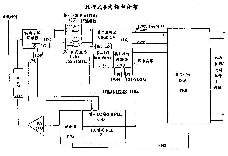
图12显示了使用被连接到参考振荡器(21)的13MHz和19.44MHz的两个晶体的解,然而,通过来自数字逻辑电路(20)的一个“选择晶体”控制信号的控制,一次只有一个晶体工作。Figure 12 shows a solution using two crystals of 13MHz and 19.44MHz connected to the reference oscillator (21), however, only one at a time is controlled by a "select crystal" control signal from the digital logic circuit (20). Crystal work.
单个中频放大器芯片包括双晶体参考振荡器(21)、第二LO及其控制PLL(17)、和双带宽第二IF放大器与第二混频器(16)。参考振荡器运行在13MHz时的一个模式,然后第二LO被控制到12×13MHz。可替换地,在第二模式,参考振荡器运行在19.44MHz上,第二LO被控制到例如155.52MHz,它足够地接近于156MHz,以致于可以使用同一个振荡器,同时它也是19.44MHz的倍数(8×19.44MHz)。A single IF amplifier chip includes a dual crystal reference oscillator (21), a second LO and its control PLL (17), and a dual bandwidth second IF amplifier and a second mixer (16). The reference oscillator runs in one mode at 13MHz, then the second LO is controlled to 12×13MHz. Alternatively, in the second mode, the reference oscillator runs at 19.44MHz and the second LO is controlled to e.g. 155.52MHz, which is close enough to 156MHz that the same oscillator can be used, which is also at 19.44MHz Multiple (8×19.44MHz).
IF放大器芯片接收来自前端芯片(12)的下变频信号,该信号通过宽带IF滤波器(15 WB)或窄带IF滤波器(15 NB)被滤波。宽带模式时的滤波器中心频率是150MHz,它与在该模式下的156MHz的第二LO进行混频,以产生6MHz的第二IF,它连同RSSI信号一起被馈送到数字信号处理器(20)。窄带第一IF滤波器运行在比155.52的第二LO高120kHz的中心频率(即155.64MHz),给出在窄带模式下120kHz的第二IF,该第二IF然后被馈送到信号处理芯片(20)。在窄带模式下120kHz或在宽带模式下6MHz的第二IF信号优选地在使用第二IF滤波器(未示出)的IF放大器(16)中被进一步滤波。在一个实施方案中,120kHz第二IF滤波器是具有大约30kHz通带宽度的集成有源带通滤波器,以及被制造成为IF放大器芯片(16,17,21)的一部分。6MHz第二IF的滤波是通过大约170kHz带宽的外部陶瓷滤波器(未示出)来实行的,正如用于电视声音IF级的滤波器那样。The IF amplifier chip receives the down-conversion signal from the front-end chip (12), and the signal is filtered through a wideband IF filter (15 WB) or a narrowband IF filter (15 NB). The filter center frequency in wideband mode is 150MHz, which is mixed with the 156MHz second LO in this mode to generate a 6MHz second IF, which is fed to the digital signal processor (20) along with the RSSI signal . The narrowband first IF filter runs at a center frequency 120kHz higher than the second LO of 155.52 (i.e. 155.64MHz), giving a second IF of 120kHz in narrowband mode, which is then fed to the signal processing chip (20 ). The second IF signal at 120 kHz in narrowband mode or 6 MHz in wideband mode is preferably further filtered in an IF amplifier (16) using a second IF filter (not shown). In one embodiment, the 120kHz second IF filter is an integrated active bandpass filter with a passband width of about 30kHz, and is fabricated as part of the IF amplifier chip (16, 17, 21). Filtering of the 6MHz second IF is performed through an external ceramic filter (not shown) of approximately 170kHz bandwidth, as is used for television sound IF stages.
当运行在800MHz的窄带AMPS模式时,双工间隔是45MHz,所以发送频率是低于第一LO的45+155.64MHz。TX偏移将是200.64MHz。然而,如图13所示,TX混频器(46)在加倍的800MHz频率对发送和接收振荡器(45,51)信号混频,因此产生401.28MHz的偏移。这与155.52MHz的第二LO具有1920kHz的最高公倍数,这样,分频器(47)把来自TX混频器(46)的TX偏移除以第一整数N2,得到第一个1920kHz信号,以及分频器(41)把来自IF芯片(30)第二LO除以整数M2=81,产生第二个1920kHz信号。两个1920kHz信号在发送相位比较器(43)中进行比较,以产生误差信号,误差信号在环路滤波器(44)中被滤波和积分,产生出用于控制TX振荡器(45)的控制信号,以便使它保持为所需要的频率,当该频率在分频器(45b)中被减半时,就成为需要的800MHz发送频率。When running in narrowband AMPS mode at 800MHz, the duplex spacing is 45MHz, so the transmit frequency is 45+155.64MHz lower than the first LO. The TX offset will be 200.64MHz. However, as shown in Figure 13, the TX mixer (46) mixes the transmit and receive oscillator (45,51) signals at a doubled 800MHz frequency, thus producing an offset of 401.28MHz. This has the highest common multiple of 1920kHz with the second LO of 155.52MHz, such that the frequency divider (47) divides the TX offset from the TX mixer (46) by a first integer N2 to obtain the first 1920kHz signal, and The frequency divider (41) divides the second LO from the IF chip (30) by the integer M2=81 to generate the second 1920kHz signal. The two 1920kHz signals are compared in the transmit phase comparator (43) to produce an error signal which is filtered and integrated in the loop filter (44) to produce the control for controlling the TX oscillator (45) signal in order to keep it at the desired frequency, which when halved in the frequency divider (45b) becomes the desired 800MHz transmit frequency.
这个在800MHz的频率规划也可被用于800MHz频段的D-AMPS模式。对于运行在1900MHz时的D-AMPS模式,双工间隔是80.04MHz,这样,发送偏移是80.04+155.64MHz=235.68MHz。这不仅仅涉及到155.52MHz的第二L0频率;然而,由于在1900MHz只使用时间双工模式,使得发送和接收发生在不同的时隙、即不同时出现,所以第一本地振荡器可以在发送和接收之间偏离240kHz的相对较小的量,以使得可以使用235.44MHz的TX偏移,而不是235.68MHz。This frequency plan at 800MHz can also be used for the D-AMPS mode in the 800MHz band. For the D-AMPS mode running at 1900MHz, the duplex interval is 80.04MHz, so the transmit offset is 80.04+155.64MHz=235.68MHz. This does not only concern the second L0 frequency at 155.52MHz; however, since only time duplexing is used at 1900MHz, so that transmission and reception occur in different time slots, i.e. not at the same time, the first local oscillator can A relatively small amount of 240kHz offset between TX and RX, so that a TX offset of 235.44MHz can be used instead of 235.68MHz.
235.44MHz的略微修正的TX偏移与155.52MHz的第二LO共用了2160kHz的公共因子。因此,在1900MHz的D-AMPS模式下,分频器(47)把235.44MHz除以重新编程的整数N2,以得到2160kHz,同时,二分频器(41)被重新编程而除以72的M2,以得出2160kHz,相位比较器(43)现在比较的信号是2160kHz,而不是1920kHz。The slightly modified TX offset of 235.44MHz shares a common factor of 2160kHz with the second LO of 155.52MHz. Therefore, in D-AMPS mode at 1900MHz, the frequency divider (47) divides 235.44MHz by the reprogrammed integer N2 to obtain 2160kHz, and at the same time, the two frequency divider (41) is reprogrammed to divide by M2 of 72 , to obtain 2160kHz, the signal compared by the phase comparator (43) is now 2160kHz instead of 1920kHz.
最后,为了得到其中双工偏移是80MHz的PCS 1900模式,发送偏移是80+150MHz,因为第一IF在该模式时是150MHz。230MHz的TX偏移与第二LO(现在是156MHz)共用2MHz的公共因子。这个模式也是时间双工的,第一LO可以被加以偏移以便把TX偏移从230MHz例如修正到234MHz,它与156MHz的第二LO具有大得多的等于78MHz的公共因子。无论如何,可以有利地保持2MHz的相位比较频率,这使得所有的相位比较频率(1920,2160和2000kHz)足够地接近,以便于使用一个公共的环路滤波器(44)和相位比较器(43)。否则,如果希望利用更大的公共因子,例如78MHz,则可能必须有不同的环路滤波器甚至相位比较器,以便去提供想要的稳定度和锁定时间的闭环特性。因此,图13的装置的重要目的在于,在所有的频段和模式粗略保持相同的TX偏移环路的环路带宽和锁定时间的工作特性。Finally, to get the
图12和13的双模式、双频段发射机-接收机假定:双超外差接收机能使用于所有的模式。在窄带AMPS和D-AMPS模式下,第二中频是120kHz,以及第二IF滤波器是装在芯片上的集成有源滤波器;在宽带PCS 1900模式下(它可包括所有的GSM话音和数据模式、卫星通信模式、和GPRS分组数据模式),第二IF是6MHz,因而第二滤波器更难以在这个频率下集成。图14上显示了用于宽带模式的另一种接收机结构,其中在宽带模式下的第二IF是零频率,也被称为“IF零拍”,它与RF零拍不同,后者是在一个变频步骤中把天线接收的频率直接变换成零频率。图14的接收机在两个步骤中把天线接收的频率变换成零频率,第一步变换到156MHz的第一中频,以及第二步通过与156MHz本地振荡器混频,从156MHz变换到零频率。由于图14的第一IF现在是156MHz,而不是图12和13的150MHz,所以对于1900MHz的TX偏移现在是156+80=236MHz,它仍旧与156MHz本地振荡器共用2MHz的公共因子。因此,图13的唯一改变是,对于PCS 1900运行的N2的数值从230/2=115改变到136/2=118。如果想要的话,可以通过把N2改变到236/4=59、把M2从78改变到39、和把M3从2改变到4而使用更高的4MHz的公共因子,或可替换地改变分数-N模数N3,以便接受用于第三相位比较器(49)的更高的参考频率。The dual-mode, dual-band transmitter-receiver of Figures 12 and 13 assumes that dual superheterodyne receivers can be used for all modes. In narrowband AMPS and D-AMPS modes, the second IF is 120kHz, and the second IF filter is an integrated active filter on-chip; in
图12、13、和14的实施方案使用两个不同的参考晶体,虽然在任何时间只使用一个晶体。无论如何,这增加了复杂性,两个晶体必须独立地进行温度补偿,因为每个晶体具有不同的单独的温度补偿要求。温度补偿是通过“自-学习”技术来实行的,由此使得接收机锁定到基站信号,然后使用基站信号频率作为校正晶体误差的基础。占优势的主要温度是通过使用热偶表测量的,加到晶体的校正值被存储在数字信号处理器(20)的微处理器存储器中的对于主要温度的表格中。The embodiments of Figures 12, 13, and 14 use two different reference crystals, although only one crystal is used at any time. Regardless, this adds to the complexity that the two crystals must be temperature compensated independently, since each crystal has different individual temperature compensation requirements. Temperature compensation is performed through a "self-learning" technique whereby the receiver locks to the base signal and then uses the base signal frequency as the basis for correcting crystal errors. The prevailing prevailing temperatures are measured using a thermocouple table and the corrections applied to the crystal are stored in a table for the prevailing temperatures in the microprocessor memory of the digital signal processor (20).
为了简化温度补偿以及减小与第二晶体有关的费用和电路板面积,有利的是考虑图15和16的使用单个晶体的解决方案。图15的解决方案是选择一个19.5MHz的折衷的晶体频率。这是13MHz的1.5倍,从该13MHz得出PCS 1900比特率,该比特率也可通过19.5MHz/72而不是13MHz/48得出。19.5MHz也接近于D-AMPS模式所需要的19.44MHz,通过把该频率除以800,可以从该频率得出24.3kS/S的符号速率。当使用19.5MHz时,误差是0.3%,这使得在发送6.667mS或162个符号持续长度的TDMA突发期间所发送的符号流中的定时漂移刚好是半个符号周期。原则上,这样的误差不大于在任何情况下由于多径传播造成传输路径延时变化必须由接收机来预计的多达一个符号的误差。无论如何,希望校正发送信号,以使得其误差不与由传播路径引入的缺陷混合。对于第一近似,符号率误差可被这样减小,即通过把晶体频率除以802,以便得到具有0.0585%的残余误差的符号速率,给出在162-符号突发持续时间内小于十分之一个符号的时间漂移。借助于跳跃计数器可以作出进一步的改进,该计数器有时除以802,有时除以803,以便建立对于24.3kS/S符号率的更精确的近似。然而,在一个实施方案中,以每比特8个样本的速率数字式地产生24.3kS/S调制。可以用每个比特若干个样本来代表已经通过使用根升余弦(root-raised-cosine)滤波器频率响应进行滤波的符号流的曲线波形。因此,通过对该晶体频率有时除以100、有时除以101,就确实可以建立对于8倍符号速率或194.4千样本/秒的精确近似。现在,将可以获得除以100的出现次数N1、和除以101的出现次数N2。In order to simplify temperature compensation and reduce the cost and board area associated with the second crystal, it is advantageous to consider the solution of FIGS. 15 and 16 using a single crystal. The solution in Figure 15 is to choose a compromise crystal frequency of 19.5MHz. This is 1.5 times the 13MHz from which the
20ms的D-AMPS帧重复周期代表19.5MHz时钟的390,000个周期,而不是19.44MHz时钟的388,800个周期。A D-AMPS frame repetition period of 20ms represents 390,000 cycles of the 19.5MHz clock, not 388,800 cycles of the 19.44MHz clock.
定时发生器因此被编程为:当使用19.5MHz时被除以390,000,而当使用19.44MHz时被除以388,800,以便建立20ms的重复周期。D-AMPS TDMA帧被划分成3个时隙,因此一个时隙是19.5MHz时钟的130,000个周期,而不是19.44MHz时钟的129,600个周期。所以,对于N1和N2的第一方程是:The timing generator is thus programmed to be divided by 390,000 when using 19.5MHz and by 388,800 when using 19.44MHz to establish a repeat period of 20ms. The D-AMPS TDMA frame is divided into 3 time slots, so a time slot is 130,000 cycles of the 19.5MHz clock, not 129,600 cycles of the 19.44MHz clock. So, the first equation for N1 and N2 is:
100.N1+101.N2=130,000100.N1+101.N2=130,000
另外,要被产生的1/8符号采样周期的总数是如前面的8×162=1296,所以,对于N1和N2的第二方程是:Additionally, the total number of 1/8 symbol sampling periods to be generated is 8×162=1296 as before, so the second equation for N1 and N2 is:
N1+N2=1296N1+N2=1296
求解这些方程,可得出N2=400,N1=896。Solving these equations gives N2=400, N1=896.
这样,跳跃计数器被编程为:除以100进行896次,以及穿插入除以101进行400次,从而产生总共1296个1/8符号周期,而定时误差不大于19.5MHz时钟的时钟周期的一半左右,或25纳秒左右。图20显示可以完成以上工作的跳跃计数器设计。分频器(100)被设计成按照来自累加器(101)的控制输入而进行除100或除101的分频,因此,使得来自分频器(100)的接连的输出脉冲将按19.5MHz时钟的100个周期或101个周期被间隔开。累加器(101)被构建为模-81累加器,这意味着,如果在加上一个增量后累加器中的数值等于或大于81,则从累加器值中减去81,并产生一个溢出脉冲或进位脉冲。从累加器(101)输出的进位脉冲被用来使得分频器(100)进行101分频。Thus, the skip counter is programmed to: divide by 100 896 times, and interleave divide by 101 400 times, resulting in a total of 1296 1/8 symbol periods with a timing error of no more than about half the clock period of the 19.5MHz clock , or around 25 ns. Figure 20 shows a jump counter design that can do the above work. The frequency divider (100) is designed to divide by 100 or by 101 according to the control input from the accumulator (101), so that successive output pulses from the frequency divider (100) will be clocked at 19.5 MHz The 100 cycles or 101 cycles are spaced apart. The accumulator (101) is built as a modulo-81 accumulator, which means that if the value in the accumulator is equal to or greater than 81 after adding an increment, 81 is subtracted from the accumulator value and an overflow occurs pulse or carry pulse. The carry pulse output from the accumulator (101) is used to divide by 101 by the frequency divider (100).
如果在由最后的分频器(100)输出脉冲使得累加器加增量后,累加器(101)没有产生进位脉冲,则分频器(100)计数100个19.5MHz时钟输入的周期,从而产生下一个输出采样速率脉冲。否则,如果最后的分频器输出脉冲使得累加器加增量和溢出,则反馈到分频器(100)的累加器进位脉冲输出使得分频器在产生下一个分频器输出采样速率脉冲以前计数101个19.5MHz时钟输入的周期。If the accumulator (101) does not generate a carry pulse after the accumulator has been incremented by the output pulse of the final divider (100), the divider (100) counts 100 cycles of the 19.5MHz clock input, thereby generating The next output sample rate pulse. Otherwise, if the last divider output pulse caused the accumulator to increment and overflow, the accumulator carry pulse output fed to the divider (100) causes the divider to Counts 101 cycles of the 19.5MHz clock input.
通过设定累加器增量等于25,累加器产生一个等于该时间的25/81的进位脉冲,它等于该时间的400/1296,这是以上用于产生D-AMPS时隙中精确数目的1296个8x符号率脉冲所需要的进行除以101的计算的那一部分。By setting the accumulator increment equal to 25, the accumulator produces a carry pulse equal to 25/81 of this time, which is equal to 400/1296 of this time, which is the 1296 used above to generate the exact number in the D-AMPS slot The part needed to perform the divide-by-101 calculation for an 8x symbol rate pulse.
图16显示使用19.5MHz的内部频率规划。在D-AMPS模式下的第一IF被改变为154.32MHz,以便分别给出对于800MHz和1900MHz下的发送相位比较器(43)的1320kHz和1080kHz频率的高的相位比较频率,同时也给出第二LO相位比较器的(31)的780kHz的高的相位比较频率。Figure 16 shows the internal frequency plan using 19.5MHz. The first IF in the D-AMPS mode is changed to 154.32MHz to give high phase comparison frequencies of 1320kHz and 1080kHz frequencies for the transmit phase comparator (43) at 800MHz and 1900MHz, respectively, while also giving the first (31) High phase comparison frequency of 780kHz for two LO phase comparators.
图17显示了本发明的再一个实施方案,这次使用一个13MHz晶体来得出所有的射频振荡器频率,以及使用一个被连接到数字芯片(20)的19.44MHz晶体,它只得出对于AMPS和D-AMPS模式的比特和数字采样速率。图18上显示了对于这种情况下的频率规划,其中与图16的唯一差别主要在于,第二LO相位比较器现在运行在520kHz。Figure 17 shows yet another embodiment of the invention, this time using a 13MHz crystal to derive all RF oscillator frequencies, and a 19.44MHz crystal connected to the digital chip (20), which derives only the frequencies for AMPS and D - Bit and digital sampling rate for AMPS mode. The frequency plan for this case is shown in Fig. 18, where the only difference from Fig. 16 is mainly that the second LO phase comparator is now running at 520kHz.
在图16和18中,主接收机综合器(第一LO)在PCS 1900模式中以模数为5(可任选地为10或20)的分数-N综合器的方式运行,而在AMPS和D-AMPS模式中以模数为12的分数-N综合器的方式运行。In Figures 16 and 18, the main receiver synthesizer (first LO) operates as a fractional-N synthesizer modulo 5 (optionally 10 or 20) in
通过使用图19的装置,有可能消除只用来产生数字时钟的19.44MHz晶体,其中数字芯片(20)当需要时可借助于其内部PLL产生它自己的19.44MHz时钟。为了便于做到这一点,分频器(41)和(42)都被分成两个分频器(41a,41b)和(42a,42b)。分频器41a在800MHz的D-AMPS模式下把164.44MHz的第二LO频率除以117,以得出发送相位比较器(43)运行时所用的1320kHz。在这个模式下,选择器开关41c被用来选择分频器41a的输出。在这个模式期间,分频器41b同时运行,除以11,以便提供14.040MHz输出给数字芯片(20)。当需要时这个频率与由数字芯片(20)借助于PLL而产生的19.44MHz共用一个1080kHz的公共因子。分频器(42a)在这时运行,以便把相位比较器(43)的工作频率除以另一个2的因子,从而得出660kHz,它连同模数-11的分数-N分频器(43)一起使用,以便提供振荡器(51)的60kHz步长,对于800MHz AMPS或D-AMPS运行情况,该振荡器(51)在除以2以后提供30kHz步长。对于1900MHzD-AMPS运行情况,开关41c选择分频器(42b)的输出,它是14.04MHz被除以13,即1080kHz。这是用于提供在1900MHz时的80.04MHz(而在800MHz时则是45MHz)的双工偏移的想要的频率。所选择的用于相位比较器(43)的1080kHz然后在可编程成除以3的分频器(49)中被除以3,从而给出用于相位比较器(49)的360kHz相位比较频率,它连同用于分频器(48)的12的分数-N模数一起使用,给出在1900MHz时的D-AMPS运行期间用于振荡器(51)的30kHz调谐步长。对于PCS1900运行,分频器(41b)被编程为除以12,对现在的156MHz的第二LO进行分频,以提供13MHz时钟输出给数字芯片(20)。在分频器(42b)中,13MHz被13分频为1MHz,这是相位比较器(43,48)的运行频率。因此,分频器(42a)被编程为使得M3=1。在这种模式下将5的分数-N模数使用于分频器(48),可提供想要的200kHz步长。By using the arrangement of Fig. 19, it is possible to eliminate the 19.44MHz crystal which is only used to generate the digital clock, where the digital chip (20) can generate its own 19.44MHz clock by means of its internal PLL when needed. To facilitate this, the frequency dividers (41) and (42) are both divided into two frequency dividers (41a, 41b) and (42a, 42b). Divider 41a divides the second LO frequency of 164.44MHz by 117 in D-AMPS mode at 800MHz to obtain 1320kHz at which the transmit phase comparator (43) operates. In this mode, selector switch 41c is used to select the output of frequency divider 41a. During this mode, the frequency divider 41b operates simultaneously, dividing by 11, to provide a 14.040MHz output to the digital chip (20). This frequency shares a common factor of 1080 kHz with the 19.44 MHz generated by the digital chip (20) by means of the PLL when required. The frequency divider (42a) operates at this time to divide the operating frequency of the phase comparator (43) by another factor of 2, thereby obtaining 660kHz, which together with the fractional-N frequency divider of the modulo-11 (43 ) to provide a 60kHz step size for the oscillator (51), which after division by 2 provides a 30kHz step size for 800MHz AMPS or D-AMPS operation. For 1900MHz D-AMPS operation, switch 41c selects the output of frequency divider (42b), which is 14.04MHz divided by 13, ie 1080kHz. This is the desired frequency to provide a duplex offset of 80.04MHz at 1900MHz (and 45MHz at 800MHz). The selected 1080kHz for the phase comparator (43) is then divided by 3 in a frequency divider (49) programmable to divide by 3, giving a 360kHz phase comparison frequency for the phase comparator (49) , which together with a fractional-N modulus of 12 for the frequency divider (48), gives a 30 kHz tuning step size for the oscillator (51) during D-AMPS operation at 1900 MHz. For PCS1900 operation, the frequency divider (41b) is programmed to divide by 12 the second LO which is now 156MHz to provide a 13MHz clock output to the digital chip (20). In the frequency divider (42b), 13MHz is divided by 13 to 1MHz, which is the operating frequency of the phase comparators (43,48). Therefore, the frequency divider (42a) is programmed such that M3=1. Using a fractional-N modulo of 5 for the frequency divider (48) in this mode provides the desired 200kHz step size.
因此,以上内容表明,本发明允许以各种方式构建使用单个晶体参考或两个晶体的双频段、双模式收发信机,以便得出270.833kB/S和24.3kS/S的交替的符号率、30kHz或200kHz的交替的信道间隔、以及45MHz、80.04MHz或80.00MHz的发送-接收双工间隔。Thus, the above shows that the present invention allows a dual-band, dual-mode transceiver using a single crystal reference or two crystals to be constructed in various ways to arrive at alternating symbol rates of 270.833 kB/S and 24.3 kS/S, Alternate channel spacing of 30kHz or 200kHz, and transmit-receive duplex spacing of 45MHz, 80.04MHz or 80.00MHz.
而且,通过比起现有技术有改进的结构所得到的这种灵活性,可允许射频硬件被实际上减小到三个集成电路芯片,它们具有在芯片之间减少了的RF互联的数目,因此使得内部干扰的风险最小化,并且减小了功率消耗。Moreover, the flexibility achieved by the improved architecture over the prior art may allow the radio frequency hardware to be reduced to virtually three integrated circuit chips with a reduced number of RF interconnections between the chips, The risk of internal interference is thus minimized and power consumption is reduced.
按照本发明的另一个方面,可以使得调谐带宽最小化。按照下面描述的示例性实施例,被馈送到超外差接收机的第一下变频器的LO,在被注入到较高频段接收机之前已被加倍。IF优选地在192和202之间进行选择,因为在这个范围以外的IF选择多半将增加公共接收VCO的所需要的调谐范围。也优选地在较高的频率端馈送用于两个接收机频段的LO。According to another aspect of the invention, the tuning bandwidth can be minimized. According to the exemplary embodiment described below, the LO fed to the first downconverter of the superheterodyne receiver is doubled before being injected into the higher band receiver. The IF is preferably chosen between 192 and 202, since an IF selection outside this range will likely increase the required tuning range of the common receive VCO. It is also preferable to feed the LOs for both receiver bands at the higher frequency end.
图21以方框图形式显示了应用双频段通信标准(例如,IS-95)的双频段接收机的一个实施方案。在这种情况下,蜂窝频段IF滤波器是30kHz宽(例如是AMPS运行情况),而PCS频段IF滤波器是1.25MHz宽(例如是CDMA运行情况)。各频段中心点优选地是在以上的频率范围内互相处于5MHz之内,以使得总的调谐不增加。Figure 21 shows, in block diagram form, one embodiment of a dual-band receiver employing a dual-band communication standard (eg, IS-95). In this case, the cellular band IF filter is 30kHz wide (eg, for AMPS operation), and the PCS band IF filter is 1.25MHz wide (eg, for CDMA operation). The band center points are preferably within 5 MHz of each other in the above frequency range so that the overall tuning does not increase.
在图21上,LO 210被馈送到超外差接收机的第一下变频器212a,b导致可以使得对于最小VCO调谐范围的IF选择最佳化的以下的方程。In FIG. 21, the
对于两个频段中的高端LO:For high-end LOs in both bands:
LOCellular=RXCellular+IFLO Cellular =RX Cellular +IF
LOPCS=RXPCS+IFLO PCS =RX PCS +IF
VCOCellular=LOCellular VCO Cellular = LO Cellular
VCOPCS=LOPCS/2VCO PCS = LO PCS /2
为了使得调谐范围最小化,VCO频率应当是来自同一组频率。为了覆盖蜂窝频段接收机,VCO应当调谐25MHz,以及为了覆盖PCS频段接收机,VCO应当调谐30MHz。所以,如果:In order to minimize the tuning range, the VCO frequencies should be from the same set of frequencies. To cover cellular band receivers, the VCO should be tuned to 25MHz, and to cover PCS band receivers, the VCO should be tuned to 30MHz. So, if:
VCOCellular=VCOPCS VCO Cellular =VCO PCS
则:LOCellular=LOPCS/2Then: LO Cellular = LO PCS /2
RXCellular+IF=(RXPCS+IF)/2RX Cellular +IF=(RX PCS +IF)/2
2*RXCellular+2*IF=RXPCS+IF2*RX Cellular +2*IF=RX PCS +IF
2*RXCellular+IF=RXPCS 2*RX Cellular +IF=RX PCS
IF=RXPCS-2*RXCellular IF=RX PCS -2*RX Cellular
由于蜂窝频段范围的跨度5MHz小于PCS频段范围,所以有一组IF频率将满足以上的要求。通过在接收范围的高端和接收范围的低端求解该方程,我们可以找到这个范围。低端关系产生以下的IF频率:Since the cellular frequency range spans 5 MHz less than the PCS frequency range, there is a set of IF frequencies that will meet the above requirements. We can find this range by solving the equation for the high end of the receptive range and the low end of the receptive range. The low-end relationship produces the following IF frequencies:
IF=RXPCS-2*RXCellular IF=RX PCS -2*RX Cellular
=1930MHz-2*869MHz=1930MHz-2*869MHz
=192MHz=192MHz
高端关系产生以下的IF频率:The high-end relationship produces the following IF frequencies:
IF=RXPCS-2*RXCellular IF=RX PCS -2*RX Cellular
=1990MHz-2*894MHz=1990MHz-2*894MHz
=202MHz=202MHz
所以,如果IF滤波器214a,b被限制为192-202MHz窗口,调谐范围可被限制为共用的接收机VCO 210的约30MHz。希望使得倍频器216可用于两个接收机的较高频段LO和高端注入。So, if the
在这个频率范围内,图22上显示了说明性实例。示例性实施例具有对于CDMA通道的192MHz的IF滤波器频率,以及对于AMPS通道的192.12MHz的IF滤波器频率。在这个实例中,第二LO是用于第一LO和发送偏移产生的参考。原则上,也可使用晶体参考。第二LO对于两个频段都是192MHz,并且被锁定到晶体参考。晶体参考可以是19.2MHz。晶体参考被除以4,从而产生4.8MHz,而第二LO被除以40,从而产生4.8MHz的公共比较频率,它应当是足够的。In this frequency range, an illustrative example is shown in Figure 22. The exemplary embodiment has an IF filter frequency of 192 MHz for CDMA channels and 192.12 MHz for AMPS channels. In this example, the second LO is the reference for the first LO and transmit offset generation. In principle, crystallographic references can also be used. The second LO is 192MHz for both bands and is locked to a crystal reference. A crystal reference could be 19.2MHz. The crystal reference is divided by 4, yielding 4.8MHz, and the second LO is divided by 40, yielding a common comparison frequency of 4.8MHz, which should be sufficient.
在PCS频段,使用第二LO作为对于第一LO的参考,第二LO可被除以384以便得到500kHz的比较频率。通过对其10分频成分数形式,第一LO可在这个频段中提供50kHz信道间隔。在蜂窝频段,使用第二LO作为对于第一LO的参考,第二LO可被除以400以便得到480kHz的比较频率。通过提供分数16分频,第一LO可在这个频段中提供30kHz信道间隔。In the PCS band, using the second LO as a reference to the first LO, the second LO can be divided by 384 to get a comparison frequency of 500 kHz. By dividing it by 10 in fractional form, the first LO provides 50kHz channel spacing in this frequency band. In the cellular band, using the second LO as a reference to the first LO, the second LO can be divided by 400 to get a comparison frequency of 480 kHz. By providing fractional divide-by-16, the first LO can provide 30kHz channel spacing in this band.
当在蜂窝频段中运行在窄带AMPS模式时,发送频率比第一LO低45.00+192.00MHz。所以,对于蜂窝频段的发送偏移是237MHz。同样地,对于在PCS频段的宽带CDMA模式的运行,发送频率比第一LO低80.00+192.00MHz。对于PCS频段的发送偏移是272MHz。使用第二LO作为用于锁定这些在PLL中的信号的参考,则将需要除以192,以用于1MHz的比较。对于PCS,发送偏移信号将必须被除以272,而对于蜂窝频段,将被除以237。在两种情况下,相位比较在1MHz下完成。When operating in narrowband AMPS mode in the cellular band, the transmit frequency is 45.00+192.00MHz lower than the first LO. So, the transmit offset for the cellular band is 237MHz. Likewise, for wideband CDMA mode operation in the PCS band, the transmit frequency is 80.00+192.00 MHz lower than the first LO. The transmit offset for the PCS band is 272MHz. Using the second LO as a reference for locking to these signals in the PLL, a division by 192 would be required for the 1 MHz comparison. The transmit offset signal will have to be divided by 272 for PCS and by 237 for cellular bands. In both cases the phase comparison is done at 1MHz.
将会看到,以上说明仅仅是一个显示现实的解可以在优选的频率范围(192-202MHz)内达到的实例。类似的设计可以用该范围内的其它频率来完成,并且晶体或第二LO被用作为参考。以上的实例包括具有显著不同的带宽的IF滤波器。这些设施仍适用于其带宽分别是200kHz和30kHz的GSM/AMPS电话。本发明对于其中两个滤波器都具有30kHz的带宽的IS-136应用项是有用的。在这种情况下,可以共用一个滤波器,而不是使用两个单独的滤波器。It will be seen that the above illustration is only an example showing that realistic solutions can be achieved within the preferred frequency range (192-202 MHz). Similar designs can be done with other frequencies in this range, and a crystal or a second LO is used as a reference. The examples above include IF filters with significantly different bandwidths. These facilities still apply to GSM/AMPS phones whose bandwidths are 200kHz and 30kHz respectively. The invention is useful for IS-136 applications where both filters have a bandwidth of 30 kHz. In this case, one filter can be shared instead of two separate filters.
因此,通过选择在192-202MHz窗口内的IF频率,调谐范围可被限制在共用的接收机VCO的30MHz。这个限制的调谐范围允许在一个3电池单元的电话[17.6]中给出类似于5电池单元的电话[20]中的VCO增益。这个电压减低的电话的同样接近的交调性能基本上与5电池单元的电话的相同,而无需任何附加电路(正如倍压器所需要的那样),它通常是5电池单元的电话中所使用的。Therefore, by choosing an IF frequency within the 192-202 MHz window, the tuning range can be limited to 30 MHz of the common receiver VCO. This limited tuning range allows a VCO gain in a 3-cell phone [17.6] similar to that in a 5-cell phone [20]. The same close intermodulation performance of this voltage-reduced phone is essentially the same as that of a 5-cell phone without any additional circuitry (as would be required for a voltage doubler), which is commonly used in 5-cell phones of.
如果在5电池单元双频段接收机中实施本发明,则VCO增益从20(75MHz/3.8V)减小到8(30MHz/3.8V)。利用这个低得多的增益,接近交调性能应当容易得多。采用不太贵的VCO可以保持同样的性能。If the invention is implemented in a 5-cell dual-band receiver, the VCO gain is reduced from 20 (75MHz/3.8V) to 8 (30MHz/3.8V). With this much lower gain, approaching intermodulation performance should be much easier. The same performance can be maintained with a less expensive VCO.
可替换地,本发明通过保持更宽的调谐范围(以及接收机接近的交调性能)和使用该额外的范围以便以电子方式将VCO的变容管校正到我们的接收机的正确范围,可导致获得较低成本的5电池单元类型的VCO。VCO是不太昂贵的,因为它是由工厂制造,而不用经过激光或机械调整。Alternatively, the present invention can be used to electronically correct the VCO's varactor to the correct range for our receiver by maintaining a wider tuning range (and close intermodulation performance of the receiver) and using this extra range to electronically correct the VCO's varactor to the correct range for our receiver. Resulting in a lower cost 5-cell type VCO. The VCO is less expensive because it is factory manufactured rather than lasered or mechanically adjusted.
因此,本发明可以得到许多相对于VCO的不明显的优点。在这个范围中的IF具有其它好处。首先,镜像滤波更容易,因为这个IF比起先前的电话所使用的(即,45MHz,72MHz,110.52MHz)更高。第二,因为IF要比接收机范围的两倍(2*60MHz或120MHz)高得多,由于它们可被滤波,接收机的1/2IF要求更容易满足。Thus, the present invention achieves many non-obvious advantages over VCOs. IFs in this range have other benefits. First, image filtering is easier because this IF is higher than what previous phones used (ie, 45MHz, 72MHz, 110.52MHz). Second, since the IF is much higher than twice the range of the receiver (2*60MHz or 120MHz), the 1/2IF requirement of the receiver is easier to meet since they can be filtered.
从实践观点出发,本发明特别适合于双频段CDMA电话。按照IS-95标准的规定,这种滤波器所需要的性能在这个频率范围中可以很容易采用SAW滤波器来满足。From a practical point of view, the invention is particularly suitable for dual-band CDMA phones. According to the IS-95 standard, the required performance of this filter can be easily satisfied by SAW filter in this frequency range.
在IS-136电话中使用本发明是较困难的,因为由该标准所需要的IF滤波在这些频率中是较难满足的。然而,高达300MHz的SAW和晶体滤波器可以使得IF滤波是也适用于IS-136标准的实际解决方案。Using the invention in IS-136 phones is more difficult because the IF filtering required by the standard is more difficult to satisfy at these frequencies. However, SAW and crystal filters up to 300MHz can make IF filtering a practical solution also for the IS-136 standard.
本发明在任何其第一和第二频段的频带中心具有大约2∶1的比值(即,其中第二频段或频带中心大约是第一频段的两倍)的双频段电话中也是有用的。The present invention is also useful in any dual-band phone in which the band centers of the first and second bands have a ratio of about 2:1 (ie, where the second band or band center is about twice as large as the first band).
本发明在其它任何希望使得振荡器调谐带宽最小化的环境中可能都是有用的。本领域技术人员可以通过使用以上教导来修改本发明,但是它们仍旧处在由以下的权利要求所描述的本发明的精神和范围内。The present invention may be useful in any other context where it is desirable to minimize the oscillator tuning bandwidth. Those skilled in the art can, by using the above teachings, modify the present invention while they remain within the spirit and scope of the invention as described by the following claims.
Claims (10)
Applications Claiming Priority (4)
| Application Number | Priority Date | Filing Date | Title |
|---|---|---|---|
| US08/974,227 | 1997-11-19 | ||
| US08/974,227 US6308048B1 (en) | 1997-11-19 | 1997-11-19 | Simplified reference frequency distribution in a mobile phone |
| US09/013,926 | 1998-01-27 | ||
| US09/013,926 US6125268A (en) | 1997-11-19 | 1998-01-27 | Tuning bandwidth minimization for low voltage dual band receiver |
Publications (1)
| Publication Number | Publication Date |
|---|---|
| CN1286830A true CN1286830A (en) | 2001-03-07 |
Family
ID=26685426
Family Applications (1)
| Application Number | Title | Priority Date | Filing Date |
|---|---|---|---|
| CN 98813194 Pending CN1286830A (en) | 1997-11-19 | 1998-11-03 | Tuning bandwidth minimization for low voltage dual band receiver |
Country Status (5)
| Country | Link |
|---|---|
| EP (1) | EP1032981B1 (en) |
| CN (1) | CN1286830A (en) |
| AU (1) | AU1372199A (en) |
| DE (1) | DE69825471D1 (en) |
| WO (1) | WO1999026352A1 (en) |
Families Citing this family (5)
| Publication number | Priority date | Publication date | Assignee | Title |
|---|---|---|---|---|
| JP4589331B2 (en) * | 2003-05-23 | 2010-12-01 | シスコ テクノロジー、インコーポレイテッド | Multimode multiband transceiver |
| TWI373925B (en) | 2004-02-10 | 2012-10-01 | Tridev Res L L C | Tunable resonant circuit, tunable voltage controlled oscillator circuit, tunable low noise amplifier circuit and method of tuning a resonant circuit |
| US7508898B2 (en) | 2004-02-10 | 2009-03-24 | Bitwave Semiconductor, Inc. | Programmable radio transceiver |
| US7672645B2 (en) | 2006-06-15 | 2010-03-02 | Bitwave Semiconductor, Inc. | Programmable transmitter architecture for non-constant and constant envelope modulation |
| CN102130697B (en) | 2010-01-20 | 2015-05-27 | 华为技术有限公司 | Receiver, transmitter and feedback device, transceiver and signal processing method |
Family Cites Families (3)
| Publication number | Priority date | Publication date | Assignee | Title |
|---|---|---|---|---|
| EP1146638B1 (en) * | 1995-05-16 | 2003-10-29 | Matsushita Electric Industrial Co., Ltd. | Wireless unit for a time division multiple access system |
| FI112133B (en) * | 1996-03-29 | 2003-10-31 | Nokia Corp | Method of forming the frequencies of a direct conversion transmitter / receiver operating in two different frequency ranges and a direct conversion transmitter / receiver of a radio communication system operating in two different frequency ranges and using the foregoing in a mobile telephone |
| FI100286B (en) * | 1996-04-01 | 1997-10-31 | Nokia Mobile Phones Ltd | Transmitter / receiver for transmitting and receiving an RF signal in two frequency ranges |
-
1998
- 1998-11-03 CN CN 98813194 patent/CN1286830A/en active Pending
- 1998-11-03 AU AU13721/99A patent/AU1372199A/en not_active Abandoned
- 1998-11-03 WO PCT/US1998/023215 patent/WO1999026352A1/en not_active Ceased
- 1998-11-03 DE DE69825471T patent/DE69825471D1/en not_active Expired - Lifetime
- 1998-11-03 EP EP98957473A patent/EP1032981B1/en not_active Expired - Lifetime
Also Published As
| Publication number | Publication date |
|---|---|
| EP1032981B1 (en) | 2004-08-04 |
| WO1999026352A1 (en) | 1999-05-27 |
| EP1032981A1 (en) | 2000-09-06 |
| AU1372199A (en) | 1999-06-07 |
| DE69825471D1 (en) | 2004-09-09 |
Similar Documents
| Publication | Publication Date | Title |
|---|---|---|
| CN1206804C (en) | Simplified Reference Frequency Assignment in Mobile Telephony | |
| CN1172542C (en) | Method and arrangement in a radio communication network | |
| US7266352B2 (en) | Multiple band RF transmitters and receivers having independently variable RF and IF local oscillators and independent high-side and low-side RF local oscillators | |
| CN101465663B (en) | Transceiver | |
| CN1500313A (en) | frequency plan | |
| CN1612490A (en) | Frequency circuit, radio frequency receiver and radio receiving-transmitting machine | |
| CN1349685A (en) | Multi-band transceiver utilizing direct conversion receiver and direct conversion receiver | |
| CN1486538A (en) | Multiband Wireless Signal Transmitter/Receiver | |
| CN1502170A (en) | Receiver and IC | |
| CN1947330A (en) | Programmable Wireless Transceiver | |
| US20090213974A1 (en) | Method for agile region and band conscious frequency planning for wireless transceivers | |
| CN1759539A (en) | Multi-band frequency synthesizer | |
| CN1531783A (en) | Separation of radio frequency devices and related methods | |
| CN1559107A (en) | Dual-band communication wireless device and local oscillation signal generation method thereof | |
| CN1286830A (en) | Tuning bandwidth minimization for low voltage dual band receiver | |
| CN1640085A (en) | 3G radio device | |
| CN1333607A (en) | Multiple frequency band transmitted/received signal generator and generating method, and transmitter and receiver | |
| EP1032982B1 (en) | Transceiver architecture in a dual band mobile phone | |
| HK1035453A (en) | Tuning bandwidth minimization for low voltage dual band receiver | |
| CN1299538A (en) | Transmitter/receiver unit | |
| CN1639990A (en) | 3G radio device | |
| HK1035447B (en) | Simplified reference frequency distribution in a mobile phone | |
| US7466968B2 (en) | Method and apparatus for providing a local oscillator signal | |
| HK1035615A (en) | Transceiver architecture in a dual band mobile phone | |
| HK1088449A (en) | Multi-band frequency synthesizer |
Legal Events
| Date | Code | Title | Description |
|---|---|---|---|
| C06 | Publication | ||
| PB01 | Publication | ||
| C10 | Entry into substantive examination | ||
| SE01 | Entry into force of request for substantive examination | ||
| C02 | Deemed withdrawal of patent application after publication (patent law 2001) | ||
| WD01 | Invention patent application deemed withdrawn after publication | ||
| REG | Reference to a national code |
Ref country code: HK Ref legal event code: WD Ref document number: 1035453 Country of ref document: HK |