CN1296830C - Starting method and system of central processing unit - Google Patents
Starting method and system of central processing unit Download PDFInfo
- Publication number
- CN1296830C CN1296830C CNB03137543XA CN03137543A CN1296830C CN 1296830 C CN1296830 C CN 1296830C CN B03137543X A CNB03137543X A CN B03137543XA CN 03137543 A CN03137543 A CN 03137543A CN 1296830 C CN1296830 C CN 1296830C
- Authority
- CN
- China
- Prior art keywords
- central processing
- processing unit
- memory
- slave
- cpu
- Prior art date
- Legal status (The legal status is an assumption and is not a legal conclusion. Google has not performed a legal analysis and makes no representation as to the accuracy of the status listed.)
- Expired - Fee Related
Links
Images


Landscapes
- Stored Programmes (AREA)
Abstract
一种中央处理单元启动的方法及系统,在多中央处理单元系统中,利用同一个存储器存放各个中央处理单元的引导程序,各个中央处理单元与该存储器之间的数据/地址总线分别通过缓冲器进行隔离;上电或整个系统复位后,主中央处理单元使得各从中央处理单元处于复位状态而无法启动,主中央处理单元给出片选信号选通对应的缓冲器及存储器,正常启动;主中央处理单元启动完毕或启动到某个步骤后,解除从中央处理单元的复位;从中央处理单元给出片选信号选通对应的缓冲器及存储器,正常启动。本发明相对于现有的从不同BOOTROM启动而言节省了成本,由于各个CPU都可以访问flash,可以很方便地实现对所有CPU的软件进行升级。

A method and system for starting a central processing unit. In a multi-central processing unit system, the same memory is used to store the boot programs of each central processing unit, and the data/address bus between each central processing unit and the memory is respectively passed through a buffer Isolation; after power-on or reset of the whole system, the main central processing unit makes each slave central processing unit in reset state and cannot be started, and the main central processing unit gives a chip select signal to strobe the corresponding buffer and memory, and starts normally; the main central processing unit After the central processing unit starts up or starts to a certain step, the reset of the slave central processing unit is released; the slave central processing unit gives a chip select signal to strobe the corresponding buffer and memory, and starts normally. Compared with the prior method of booting from different BOOTROMs, the present invention saves costs, and since each CPU can access flash, it can conveniently upgrade the software of all CPUs.
Description
技术领域technical field
本发明涉及电数字数据处理,尤其涉及一种中央处理单元(CPU)启动的方法及系统。The invention relates to electrical digital data processing, in particular to a method and system for starting a central processing unit (CPU).
背景技术Background technique
现在中央处理单元(CPU)启动都有单独的启动系统,特别是在多CPU系统中,每个CPU由各自的启动芯片(BOOTROM)启动,这样的设计方式使用的器件数量多,而且不易实现BOOTROM软件升级,造成系统维护和增强功能的困难。Now the central processing unit (CPU) has a separate boot system, especially in a multi-CPU system, each CPU is started by its own boot chip (BOOTROM). This design method uses a large number of devices, and it is not easy to implement BOOTROM. Software upgrades cause difficulties in system maintenance and enhanced functions.
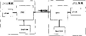
如图1所示,在现有技术方案中,各个CPU系统(如图中CPU1系统和CPU2系统)都有独立的BOOTROM,系统只能从该CPU对应的BOOTROM启动。由于整个系统中,通常只以某个CPU为主,其他CPU协助处理业务,各CPU之间只进行简单的通信,系统设计中为了降低成本,一般只实现主CPU的BOOTROM升级,而各个从CPU的BOOTROM不升级。如果实现所有BOOTROM的升级,则需要为每个BOOTROM设计加载电路,系统设计复杂度增加,成本上升。As shown in FIG. 1 , in the prior art solution, each CPU system (such as the CPU1 system and the CPU2 system in the figure) has an independent BOOTROM, and the system can only be started from the BOOTROM corresponding to the CPU. Because in the whole system, usually only one CPU is the main one, and other CPUs assist in processing business, and only simple communication is carried out between each CPU. The BOOTROM is not upgraded. If all BOOTROMs are upgraded, it is necessary to design and load circuits for each BOOTROM, which increases system design complexity and costs.
现有技术方案的缺点为:The disadvantages of prior art solutions are:
(1)在多CPU系统中,每个CPU通道由各自独立的BOOTROM引导启动,系统中需要使用多个BOOTROM存储器,增加了系统成本。(1) In a multi-CPU system, each CPU channel is booted and started by its own independent BOOTROM, and multiple BOOTROM memories need to be used in the system, which increases the system cost.
(2)系统需要升级所有CPU的软件时,为降低成本,只实现主CPU的升级,从CPU不升级。(2) When the system needs to upgrade the software of all CPUs, in order to reduce costs, only the main CPU is upgraded, and the slave CPUs are not upgraded.
(3)实现从CPU升级需要增加系统复杂度,增加系统成本。(3) Upgrading from a CPU needs to increase system complexity and system cost.
发明内容Contents of the invention
本发明所要解决的技术问题是:克服现有技术各个CPU通过独立的BOOTROM启动所带来的成本高、升级复杂等缺点,提供一种CPU启动的方法和系统,从而降低系统成本,并方便实现CPU的升级。The technical problem to be solved by the present invention is: to overcome the disadvantages of high cost and complicated upgrading caused by starting each CPU through an independent BOOTROM in the prior art, and provide a method and system for starting the CPU, thereby reducing system cost and facilitating implementation CPU upgrades.
本发明为解决上述技术问题所采用的技术方案为:The technical scheme that the present invention adopts for solving the problems of the technologies described above is:
这种中央处理单元启动的方法,在多中央处理单元系统中,利用同一个存储器存放各个中央处理单元的引导程序,各个中央处理单元与该存储器之间的数据/地址总线分别通过缓冲器进行隔离;中央处理单元系统启动流程步骤如下:This method of starting the central processing unit, in a multi-central processing unit system, utilizes the same memory to store the boot programs of each central processing unit, and the data/address buses between each central processing unit and the memory are isolated through buffers ; The steps of the central processing unit system startup process are as follows:
1)上电或整个系统复位后,主中央处理单元使得各从中央处理单元处于复位状态而无法启动,主中央处理单元给出片选信号选通与主中央处理单元对应的缓冲器及存储器,正常启动;1) After power-on or whole system reset, the main central processing unit makes each slave central processing unit in reset state and cannot be started, and the main central processing unit gives a chip select signal to strobe the buffer and memory corresponding to the main central processing unit, Normal start;
2)主中央处理单元启动完毕或启动到某个步骤后,解除从中央处理单元的复位,并调整主中央处理单元输出的控制信号,使得从中央处理单元可以访问存储器;2) After the main central processing unit is started or started to a certain step, release the reset of the slave central processing unit, and adjust the control signal output by the main central processing unit, so that the slave central processing unit can access the memory;
3)从中央处理单元给出片选信号选通该从中央处理单元对应的缓冲器及存储器,正常启动。3) The slave central processing unit sends a chip select signal to select the corresponding buffer and memory of the slave central processing unit, and starts normally.
其中,所述的存储器可采用闪存,各个中央处理单元的引导程序和应用软件在同一个闪存中根据地址划分存放在不同的空间。Wherein, the memory may be a flash memory, and the boot programs and application software of each central processing unit are stored in different spaces according to addresses in the same flash memory.
其中,从中央处理单元已正常启动或启动到不需要存储器后,主中央处理单元可以通过调整其输出的控制信号,取消从中央处理单元选通该从中央处理单元对应的缓冲器的权限,防止从中央处理单元误访问存储器。Wherein, after the slave central processing unit has been normally started or started to no need of memory, the main central processing unit can cancel the authority of the slave central processing unit to gate the buffer corresponding to the slave central processing unit by adjusting the control signal output by it, preventing Misaccess to memory from central processing unit.
其中,所述的从中央处理单元已正常启动的信息通过中央处理单元之间的通信通道获得,也可以估算一定的时间,确保该从中央处理单元已正常启动或已启动到不需要存储器的阶段。Wherein, the information that the said slave central processing unit has been started normally is obtained through the communication channel between the central processing units, and a certain period of time can also be estimated to ensure that the slave central processing unit has been started normally or has been started to a stage where no memory is required .
其中,在各中央处理单元正常运行期间,如果从中央处理单元需要访问存储器,必须通过中央处理单元之间的通信通道向主中央处理单元提出申请,得到允许后,主中央处理单元调整其输出的控制信号,使该从中央处理单元可以选通读取存储器;读取完毕后通知主中央处理单元,主中央处理单元调整其输出的控制信号,取消该从中央处理单元选通读取存储器的权限。Among them, during the normal operation of each central processing unit, if the secondary central processing unit needs to access the memory, it must apply to the main central processing unit through the communication channel between the central processing units. After being allowed, the main central processing unit adjusts its output control signal, so that the slave central processing unit can strobe and read the memory; after reading, notify the main central processing unit, and the master central processing unit adjusts the control signal output by it, and cancels the permission of the slave central processing unit to strobe and read the memory .
其中,如果存储器的空间较大,某些中央处理单元的地址范围不够时,根据该中央处理单元程序在存储器中存放的地址,在缓冲器之前给高位的存储器地址线做上、下拉处理,将其从外部强制成所需的固定电平,使得该中央处理单元可以访问到分配的存储器空间。Wherein, if the space of the memory is large, when the address range of some central processing units is not enough, according to the address stored in the memory by the central processing unit program, before the buffer, the high-order memory address lines are processed to be pulled up and down. It is externally forced to the required fixed level so that the central processing unit can access the allocated memory space.
相应的一种中央处理单元启动系统,其特征在于:A corresponding central processing unit startup system is characterized in that:
主、从中央处理单元的数据/地址总线分别通过缓冲器隔离后连接到同一存储器;The data/address buses of the master and slave central processing units are respectively separated by buffers and connected to the same memory;
主中央处理单元的片选信号直接输入到与主中央处理单元对应的缓冲器的使能信号管脚,同时该片选信号在与各从中央处理单元的片选信号相与后输入存储器,控制存储器的选通;The chip selection signal of the main central processing unit is directly input to the enable signal pin of the buffer corresponding to the main central processing unit, and the chip selection signal is input into the memory after being phased with the chip selection signals of each slave central processing unit, and the control memory gating;
从中央处理单元的片选信号在与所述主中央处理单元的片选信号相与之前,由上拉电阻拉高,并被与该从中央处理单元对应的缓冲器隔离;Before the chip select signal of the slave central processing unit is ANDed with the chip select signal of the master central processing unit, it is pulled up by a pull-up resistor and isolated from the buffer corresponding to the slave central processing unit;
主中央处理单元复位信号经下拉电阻拉低后输出到各从中央处理单元的复位管脚,同时,该复位信号在进行非运算后,与经上拉电阻拉高的主中央处理单元输出的控制信号及从中央处理单元的片选信号进行或运算,所产生的信号输入该从中央处理单元对应的缓冲器的使能信号管脚。The main central processing unit reset signal is output to the reset pins of each slave central processing unit after being pulled low by the pull-down resistor. OR operation is performed on the signal and the chip select signal of the slave central processing unit, and the generated signal is input to the enable signal pin of the buffer corresponding to the slave central processing unit.
其中,所述的存储器可以是具有块保护功能的闪存器件。Wherein, the memory may be a flash memory device with a block protection function.
其中,主、从中央处理单元之间可通过通信通道相连进行通讯。Wherein, the master and slave central processing units can be connected through a communication channel for communication.
其中,各中央处理单元的数据/地址总线还分别连接同步动态存储器或其它存储器件。Wherein, the data/address bus of each central processing unit is also respectively connected to a synchronous dynamic memory or other storage devices.
本发明的有益效果为:本发明在多CPU系统中使用flash来放置各CPU的引导程序和应用软件,所有CPU共用一个flash,从同一个flash启动,相对于现有技术从不同的BOOTROM启动而言节省了成本,由于各个CPU都可以访问flash,可以很方便地实现对所有CPU的软件进行升级。The beneficial effect of the present invention is: the present invention uses flash to place the guide program and application software of each CPU in the multi-CPU system, all CPUs share a flash, start from the same flash, start from different BOOTROM with respect to prior art This saves the cost, and because each CPU can access the flash, it is very convenient to upgrade the software of all CPUs.
附图说明Description of drawings
图1为现有的CPU启动原理示意图;FIG. 1 is a schematic diagram of an existing CPU startup principle;
图2为本发明CPU启动原理示意图;Fig. 2 is the schematic diagram of CPU startup principle of the present invention;
图3为本发明多个CPU从同一个flash启动的控制电路图;Fig. 3 is the control circuit diagram that multiple CPUs of the present invention start from the same flash;
图4为本发明CPU启动流程图;Fig. 4 is a CPU startup flow chart of the present invention;
图5为本发明CPU地址线范围不足时的处理示意图。FIG. 5 is a schematic diagram of processing when the CPU address line range is insufficient in the present invention.
具体实施方式Detailed ways
下面根据附图和实施例对本发明作进一步详细说明:Below according to accompanying drawing and embodiment the present invention will be described in further detail:
如图2所示为本发明CPU启动原理示意图,本发明使用可读写的存储器(如flash闪存器件)作为载体,取代现有的启动芯片(bootrom),使用flash器件存放CPU软件,所有CPU共用同一个flash,从同一个flash启动。由于CPU启动时读取bootrom的时间很短,程序搬运到同步动态存储器(sdram)后不再访问bootrom,所以可以通过主CPU来控制各个CPU系统对bootrom按顺序先后访问,达到共享的目的。为防止各CPU随意选取通flash以及隔离各个总线防止干扰,各个CPU系统与flash之间的数据/地址总线、及部分或所有片选信号通过缓冲器(buffer)进行隔离,由主CPU(图中CPU1)对各buffer进行控制,实现各CPU对flash的先后访问。同时主CPU可以在正常运行时选通flash,进行各个CPU软件的升级加载。As shown in Figure 2, it is a schematic diagram of the CPU starting principle of the present invention. The present invention uses a readable and writable memory (such as a flash flash memory device) as a carrier to replace the existing boot chip (bootrom), and uses the flash device to store CPU software, which is shared by all CPUs. The same flash, boot from the same flash. Since the time for reading the bootrom when the CPU starts is very short, the program will not access the bootrom after being transferred to the synchronous dynamic memory (sdram), so the main CPU can be used to control each CPU system to access the bootrom sequentially to achieve the purpose of sharing. In order to prevent each CPU from randomly selecting the flash and isolating each bus to prevent interference, the data/address bus between each CPU system and the flash, and some or all chip select signals are isolated through a buffer (buffer), which is controlled by the main CPU (in the figure). CPU1) controls each buffer, and realizes the sequential access of each CPU to the flash. At the same time, the main CPU can strobe the flash during normal operation to upgrade and load the software of each CPU.
如图3所示,以两个CPU系统为例说明本发明的技术方案,图中CPU1为主CPU,CPU2为从CPU。CPU1、CPU2的数字地址总线接口(date_addr_bus)分别经buffer1、buffer2的隔离后与同一flash的数字地址总线接口(date_addr_bus)相接。在buffer和flash分别选通时,相应的CPU可以访问flash,从flash的相应区域读取数据和进行数据搬运到相应的SDRAM,从而启动。As shown in FIG. 3 , the technical solution of the present invention is described by taking two CPU systems as an example. In the figure, CPU1 is the master CPU, and CPU2 is the slave CPU. The digital address bus interfaces (date_addr_bus) of CPU1 and CPU2 are connected to the digital address bus interface (date_addr_bus) of the same flash after being isolated by buffer1 and buffer2 respectively. When the buffer and the flash are selected respectively, the corresponding CPU can access the flash, read data from the corresponding area of the flash and transfer the data to the corresponding SDRAM, thereby starting.
图3中,缓冲器buffer1和buffer2的/G管脚为开关选通信号,低有效。该管脚为高时,相应的CPU和flash的数据/地址总线隔离;该管脚为低时,相应的CPU和flash的数据/地址总线连通。In FIG. 3 , the /G pins of the buffers buffer1 and buffer2 are switch gating signals, which are active low. When the pin is high, the corresponding CPU and the flash data/address bus are isolated; when the pin is low, the corresponding CPU and the flash data/address bus are connected.
各CPU之间的通信通道在不同的系统中可以不同,可以为RS232、RS485、I2C等串口;也可以为其他接口,如通用测试与操作接口(UTOPIA)等;也可以为自定义的通信接口。The communication channel between each CPU can be different in different systems, it can be serial ports such as RS232, RS485, I2C; it can also be other interfaces, such as the universal test and operation interface (UTOPIA), etc.; it can also be a self-defined communication interface .
CPU1的片选信号/CS1直接输入buffer1的/G管脚,同时/CS1在与CPU2的片选信号/CS2相与(and)后形成flash的选通信号/CS3。The chip select signal /CS1 of CPU1 is directly input to the /G pin of buffer1, and at the same time /CS1 is ANDed with the chip select signal /CS2 of CPU2 to form the strobe signal /CS3 of the flash.
CPU2的片选信号/CS2在做与运算送给flash之前,通过buffer2隔离,防止CPU2不取得flash控制权时选通flash。/cs2_buf的上拉电阻保证上电期间和buffer2隔离时,该信号为高状态,不会误选通flash。The chip select signal /CS2 of CPU2 is isolated by buffer2 before it is sent to the flash through AND operation, so as to prevent CPU2 from strobing the flash when it does not obtain the control right of the flash. The pull-up resistor of /cs2_buf ensures that when it is isolated from buffer2 during power-on, the signal is in a high state, and the flash will not be selected by mistake.
CPU1的复位输出信号/reset_out连到CPU2的复位管脚/reset,控制CPU2的复位状态。如果有多个从CPU,每个从CPU各需要一个与主CPU相连的复位信号,不能共用,复位信号低有效。The reset output signal /reset_out of CPU1 is connected to the reset pin /reset of CPU2 to control the reset state of CPU2. If there are multiple slave CPUs, each slave CPU needs a reset signal connected to the master CPU, which cannot be shared, and the reset signal is low and effective.
CPU1的control信号先和/reset_out的非(not)进行或运算(or)后产生信号CPU1_ctr,再将CPU1-ctr与/cs2进行或运算后输出CPU2_OE信号到buffer2的/G管脚,CPU2_OE作为使能信号控制buffer2的通断,防止CPU2随意选通buffer2,访问flash。平时由于上拉电阻的上拉,control信号为高,不允许CPU2选通buffer2。允许CPU2选通buffer2时,control信号为低。上拉电阻保证上电期间control信号为高状态。The control signal of CPU1 is ORed with the not (not) of /reset_out first to generate the signal CPU1_ctr, and then the CPU1-ctr is ORed with /cs2 to output the CPU2_OE signal to the /G pin of buffer2, and CPU2_OE is used as the The signal can control the on-off of buffer2 to prevent CPU2 from randomly selecting buffer2 and accessing flash. Normally, due to the pull-up of the pull-up resistor, the control signal is high, and CPU2 is not allowed to select buffer2. When CPU2 is allowed to strobe buffer2, the control signal is low. The pull-up resistor ensures that the control signal is in a high state during power-up.
这样,当系统启动时,各CPU的启动过程如下(假设以下器件的控制信号都为低有效):In this way, when the system starts, the startup process of each CPU is as follows (assuming that the control signals of the following devices are all active low):
上电后或整个系统复位后,CPU1先正常启动,CPU1的/reset_out管脚输出低电平,使得CPU2的复位输入为低(同时该管脚被拉低,保证CPU1启动初期也能为低电平),CPU2处于复位状态,无法启动;同时/reset_out经过非和或运算后使得CPU2_OE为高,关闭buffer2。CPU1正常启动,给出/CS1低信号,/CS1输入buffer1的/G管脚选通buffer1,同时/CS1与/CS2_buf目与产生低信号/CS3送入flash,选取通flash,取得flash的读写权限,从flash的相应区域读取数据和进行数据搬运到SDRAM。After power-on or after the whole system is reset, CPU1 starts normally first, and the /reset_out pin of CPU1 outputs a low level, making the reset input of CPU2 low (at the same time, the pin is pulled low to ensure that CPU1 can also be low-powered at the beginning of startup. level), CPU2 is in the reset state and cannot be started; at the same time, /reset_out makes CPU2_OE high after NOR operation, and closes buffer2. CPU1 starts up normally, gives /CS1 low signal, /G pin of /CS1 input buffer1 selects buffer1, at the same time, /CS1 and /CS2_buf generate low signal /CS3 sends to flash, selects pass flash, obtains flash reading and writing Permission to read data from the corresponding area of flash and transfer data to SDRAM.
CPU1启动完毕或者启动到某个步骤后(根据实际情况决定),/reset_out管脚拉高,使得CPU2走出复位状态,正常启动,同时control信号保持为低电平,使得CPU2可以控制buffer2的选通。CPU2正常启动,给出/CS2低信号,输入/G管脚的信号为低,buffer2选通,输出/CS2_buf为低,从而选通flash,取得flash的读写权限,从flash的相应区域读取数据和进行数据搬运到SDRAM。After CPU1 starts up or starts to a certain step (determined according to the actual situation), the /reset_out pin is pulled high, so that CPU2 goes out of the reset state and starts normally, and at the same time the control signal remains low, so that CPU2 can control the gating of buffer2 . CPU2 starts up normally, gives a /CS2 low signal, the signal of the input /G pin is low, buffer2 is strobed, and the output /CS2_buf is low, thereby strobes the flash, obtains the read and write permission of the flash, and reads from the corresponding area of the flash data and perform data transfer to SDRAM.
在CPU2启动期间,CPU1必须保证不访问flash,以免发生冲突。CPU2启动完毕的信息可以通过CPU之间的通信通道获得,也可以估算一定的时间,确保CPU2已正常启动或已启动到不需要flash的阶段(CPU从flash启动的时间通常很短,几秒钟之内可以完成基本启动,不再需要从flash读取数据)。确保CPU2不再需要flash后,CPU1的control管脚拉高,取消CPU2选通buffer2的权限,防止两个CPU同时访问flash,造成冲突,损坏器件。During CPU2 startup, CPU1 must ensure that it does not access flash to avoid conflicts. The information about the completion of CPU2 startup can be obtained through the communication channel between CPUs, and a certain period of time can also be estimated to ensure that CPU2 has started normally or has started to a stage that does not require flash (the time for CPU to start from flash is usually very short, a few seconds The basic startup can be completed within , no longer need to read data from flash). After ensuring that CPU2 no longer needs the flash, the control pin of CPU1 is pulled high to cancel the permission of CPU2 to select buffer2, so as to prevent two CPUs from accessing the flash at the same time, causing conflicts and damaging the device.
在正常运行期间,如果CPU2需要访问flash,必须通过CPU之间的通信通道提出申请,得到允许后同时CPU1的control管脚拉低,CPU2可以选通读取flash。读取完毕后通知CPU1,CPU1的control管脚拉高,取消CPU2选通buffer2的权限。如果正常运行期间CPU2不需要访问flash,没有本操作。During normal operation, if CPU2 needs to access the flash, it must apply through the communication channel between the CPUs. After getting permission, the control pin of CPU1 is pulled low at the same time, and CPU2 can strobe to read the flash. After reading, notify CPU1, pull the control pin of CPU1 high, and cancel the permission of CPU2 to select buffer2. If CPU2 does not need to access flash during normal operation, there is no such operation.
图3中只给出了三个片选信号:/cs1为主CPU给flash的片选信号(输出),/cs2为从CPU给flash的片选信号(输出),/cs3为flash的选通信号(输入)。Only three chip selection signals are shown in Figure 3: /cs1 is the chip selection signal (output) from the main CPU to the flash, /cs2 is the chip selection signal (output) from the CPU to the flash, and /cs3 is the selection communication of the flash number (input).
当从CPU不只CPU2一个时,同样根据control、/reset_out和从CPU给出的片选信号作为使能信号输入相应buffer的/G管脚来控制该buffer的通断,并通过该从CPU给出的片选信号与主CPU给出的片选信号相与来控制flash的通断,从而实现该从CPU对flash的访问。为了安全起见,也可以增加主CPU的control信号来控制相应的从CPU,达到主CPU可以单独控制各个从CPU的buffer通断。When there is more than one CPU2 from the CPU, the chip select signal given by control, /reset_out and the slave CPU is also used as the enable signal to input the /G pin of the corresponding buffer to control the on-off of the buffer, and through the slave CPU. The chip select signal and the chip select signal given by the main CPU control the on and off of the flash, so as to realize the access of the slave CPU to the flash. For safety reasons, the control signal of the master CPU can also be increased to control the corresponding slave CPUs, so that the master CPU can independently control the buffer on and off of each slave CPU.
如图4所示为本发明CPU启动流程图,启动流程概括如下:As shown in Figure 4, it is the CPU startup flowchart of the present invention, and the startup procedure is summarized as follows:
1)上电或整个系统复位后,主CPU使得各从CPU处于复位状态而无法启动,主CPU给出片选信号选通主CPU与flash之间的buffer及flash,正常启动;1) After the power is turned on or the whole system is reset, the main CPU makes each slave CPU in the reset state and cannot be started, and the main CPU sends a chip select signal to select the buffer and flash between the main CPU and the flash, and starts normally;
2)主CPU启动完毕或启动到某个步骤后,解除从CPU的复位,并把control信号拉低,使得从CPU可以访问flash;2) After the main CPU is started or started to a certain step, release the reset of the slave CPU, and pull down the control signal, so that the slave CPU can access the flash;
3)从CPU给出片选信号选通该从CPU与flash之间的buffer及flash,正常启动,在此期间主CPU不能访问flash;3) The slave CPU gives a chip select signal to strobe the buffer and flash between the slave CPU and the flash, and starts normally, during which the main CPU cannot access the flash;
4)确保从CPU不再访问flash后,主CPU把control信号拉高,防止从CPU误访问flash;4) After ensuring that the slave CPU no longer accesses the flash, the master CPU pulls the control signal high to prevent the slave CPU from accidentally accessing the flash;
5)主CPU和从CPU完成其它启动操作;5) The main CPU and the slave CPU complete other startup operations;
6)主CPU和从CPU正常运行。6) The master CPU and slave CPU are running normally.
本系统中的flash空间要进行划分,给各个CPU划分足够的地址空间,放置软件和其他信息。由于各个CPU都可以访问flash,可以很方便的实现在线加载各个软件,升级各个CPU的软件。The flash space in this system should be divided to divide enough address space for each CPU to place software and other information. Since each CPU can access the flash, it is very convenient to load each software online and upgrade the software of each CPU.
如果flash的空间较大,某些CPU的地址范围不够时,可以采用在buffer之前给高位的flash地址线做上、下拉处理,通过上、下拉处理后,从外部将高位的地址线强制成所需的固定电平,使得该CPU可以访问到分配的flash空间。如图5所示,当CPU地址线为A0-A18,共19根,而flash地址线为A0-A20,共21根时,图4圈中部分采用上、下拉处理,根据该CPU在flash中存储的地址,在buffer之前将A19强制为低电平,A20强制为高电平,从而在buffer选通时,该CPU可以访问到分配的flash空间(0x100000-0x17FFFF的512k空间分配给该从CPU使用)。If the flash space is large and the address range of some CPUs is not enough, you can use the high-order flash address line to do up and pull-down processing before the buffer. The required fixed level allows the CPU to access the allocated flash space. As shown in Figure 5, when the CPU address lines are A0-A18, a total of 19, and the flash address lines are A0-A20, a total of 21, the part in the circle in Figure 4 adopts up and down processing, according to the CPU in the flash The stored address, A19 is forced to be low level before the buffer, and A20 is forced to be high level, so that when the buffer is selected, the CPU can access the allocated flash space (512k space of 0x100000-0x17FFFF is allocated to the slave CPU use).
如果某些CPU的数据线宽不够,比如flash为16bit的数据线,而从CPU1为8位的数据线时,则该CPU只能访问8位对应的flash空间。If the data line width of some CPUs is not enough, for example, the flash is a 16-bit data line, and the slave CPU1 is an 8-bit data line, the CPU can only access the flash space corresponding to 8 bits.
本发明节省了成本,降低了系统复杂度,同时可以很方便的实现对所有CPU的软件进行升级,只要能访问flash器件的CPU都能升级软件。通常主CPU能够访问flash器件的所有空间,同时它能够决定flash器件的使用权限,由它来升级软件比较简单方便。需要注意的是,由于基本输入输出系统(BIOS)软件部分软件比较重要,可选用具有块保护功能的flash器件,从而可在平时使得各个CPU的BIOS软件空间处于保护状态,防止误操作。The invention saves cost, reduces system complexity, and can conveniently upgrade the software of all CPUs, as long as the CPUs that can access the flash device can upgrade the software. Usually the main CPU can access all the space of the flash device, and it can determine the usage authority of the flash device at the same time. It is relatively simple and convenient to upgrade the software by it. It should be noted that due to the important part of the basic input and output system (BIOS) software, a flash device with block protection function can be selected, so that the BIOS software space of each CPU can be in a protected state at ordinary times to prevent misuse.
Claims (10)
Priority Applications (1)
| Application Number | Priority Date | Filing Date | Title |
|---|---|---|---|
| CNB03137543XA CN1296830C (en) | 2003-06-08 | 2003-06-08 | Starting method and system of central processing unit |
Applications Claiming Priority (1)
| Application Number | Priority Date | Filing Date | Title |
|---|---|---|---|
| CNB03137543XA CN1296830C (en) | 2003-06-08 | 2003-06-08 | Starting method and system of central processing unit |
Publications (2)
| Publication Number | Publication Date |
|---|---|
| CN1553338A CN1553338A (en) | 2004-12-08 |
| CN1296830C true CN1296830C (en) | 2007-01-24 |
Family
ID=34323575
Family Applications (1)
| Application Number | Title | Priority Date | Filing Date |
|---|---|---|---|
| CNB03137543XA Expired - Fee Related CN1296830C (en) | 2003-06-08 | 2003-06-08 | Starting method and system of central processing unit |
Country Status (1)
| Country | Link |
|---|---|
| CN (1) | CN1296830C (en) |
Families Citing this family (17)
| Publication number | Priority date | Publication date | Assignee | Title |
|---|---|---|---|---|
| TWI308696B (en) | 2005-10-07 | 2009-04-11 | Via Tech Inc | Initializing method bus device |
| CN100373365C (en) * | 2005-10-14 | 2008-03-05 | 威盛电子股份有限公司 | Bus component initialization method |
| CN101222373B (en) * | 2008-01-29 | 2010-07-28 | 杭州华三通信技术有限公司 | Multi-master control system and master control board starting method thereof |
| CN102520778A (en) * | 2011-12-09 | 2012-06-27 | 山东大学 | One-key reset method suitable for embedded Linux operating system |
| CN102647280A (en) * | 2012-02-28 | 2012-08-22 | 山东大学 | Embedded Internet access device for community information system and its realization method |
| CN103907108B (en) * | 2012-10-25 | 2017-07-07 | 华为技术有限公司 | Share method, controller and the system of flash memory |
| CN103150224B (en) * | 2013-03-11 | 2015-11-11 | 杭州华三通信技术有限公司 | For improving the electronic equipment and method that start reliability |
| JP5996513B2 (en) * | 2013-11-27 | 2016-09-21 | 京セラドキュメントソリューションズ株式会社 | Electronics |
| CN104750510B (en) * | 2013-12-30 | 2019-04-02 | 深圳市中兴微电子技术有限公司 | A kind of chip starting method and multi-core processor chip |
| CN104834535A (en) * | 2014-02-07 | 2015-08-12 | 昆达电脑科技(昆山)有限公司 | SOC (System On Chip) chip system and power on method thereof |
| CN105468390B (en) * | 2014-09-05 | 2020-11-06 | 中兴通讯股份有限公司 | BOOT online upgrading device and method |
| CN106407156B (en) * | 2016-09-23 | 2018-11-23 | 深圳震有科技股份有限公司 | The method and system of one BOOTROM guidance multi-core CPU starting |
| CN108268286A (en) * | 2016-12-29 | 2018-07-10 | 联想(上海)信息技术有限公司 | Computer system starting method and computer system |
| CN109273031B (en) * | 2018-10-09 | 2021-07-27 | 珠海格力电器股份有限公司 | Flash decoding circuit and flash decoding method |
| CN109800032B (en) * | 2019-01-31 | 2022-03-25 | 深圳忆联信息系统有限公司 | BOOTROM multi-core loading method and device |
| CN110119286A (en) * | 2019-04-11 | 2019-08-13 | 厦门亿联网络技术股份有限公司 | A kind of firmware guidance implementation method based on simulation Flash chip |
| CN120523770A (en) * | 2024-02-22 | 2025-08-22 | 华为技术有限公司 | Chip system, operation method, data processing board and electronic equipment |
Citations (2)
| Publication number | Priority date | Publication date | Assignee | Title |
|---|---|---|---|---|
| CA2069972A1 (en) * | 1991-08-30 | 1993-03-01 | Brigitte R. Rapatz | Power-up and initialization of a multiprocessor system |
| US5497497A (en) * | 1989-11-03 | 1996-03-05 | Compaq Computer Corp. | Method and apparatus for resetting multiple processors using a common ROM |
-
2003
- 2003-06-08 CN CNB03137543XA patent/CN1296830C/en not_active Expired - Fee Related
Patent Citations (2)
| Publication number | Priority date | Publication date | Assignee | Title |
|---|---|---|---|---|
| US5497497A (en) * | 1989-11-03 | 1996-03-05 | Compaq Computer Corp. | Method and apparatus for resetting multiple processors using a common ROM |
| CA2069972A1 (en) * | 1991-08-30 | 1993-03-01 | Brigitte R. Rapatz | Power-up and initialization of a multiprocessor system |
Also Published As
| Publication number | Publication date |
|---|---|
| CN1553338A (en) | 2004-12-08 |
Similar Documents
| Publication | Publication Date | Title |
|---|---|---|
| CN1296830C (en) | Starting method and system of central processing unit | |
| CN112783818B (en) | On-line upgrading method and system of multi-core embedded system | |
| AU651747B2 (en) | Arbitration control logic for computer system having dual bus architecture | |
| US7287101B2 (en) | Direct memory access using memory descriptor list | |
| CN1085864C (en) | Add-in board with enable/disable expansion ROM for PCI bus computer | |
| US6789169B2 (en) | Embedded DRAM cache memory and method having reduced latency | |
| CN1026926C (en) | A data processing system for dynamically setting each time scale in a dynamic storage system | |
| US6202107B1 (en) | Host controller interface descriptor fetching unit | |
| JP6777050B2 (en) | Virtualization systems, virtualization programs, and storage media | |
| US7581054B2 (en) | Data processing system | |
| CN116342365A (en) | Techniques for expanding system memory via use of available device memory | |
| JPH096722A (en) | Computer system | |
| US7934029B2 (en) | Data transfer between devices within an integrated circuit | |
| CN108121672A (en) | A kind of storage array control method and device based on Nand Flash memorizer multichannel | |
| KR20120092176A (en) | Method and system for entirety mutual access in multi-processor | |
| CN105264506A (en) | Assigning processors to memory mapped configuration | |
| US20190138341A1 (en) | Method and apparatus for managing disaggregated memory | |
| US20260037185A1 (en) | Heterogeneous in-storage computation | |
| CN115309678B (en) | Processing system, related integrated circuit, device and method | |
| CN118427131B (en) | Dynamic allocation method and system for chip storage of multi-core system | |
| JPH08227381A (en) | Memory system and method of accessing this system | |
| CN119938576B (en) | APB bus-based communication management methods, apparatus, devices, and storage media | |
| US5799195A (en) | Structure and method for detecting occurrence of external events using semaphores | |
| US8244994B1 (en) | Cooperating memory controllers that share data bus terminals for accessing wide external devices | |
| US9436617B2 (en) | Dynamic processor-memory revectoring architecture |
Legal Events
| Date | Code | Title | Description |
|---|---|---|---|
| C06 | Publication | ||
| PB01 | Publication | ||
| C10 | Entry into substantive examination | ||
| SE01 | Entry into force of request for substantive examination | ||
| C14 | Grant of patent or utility model | ||
| GR01 | Patent grant | ||
| CF01 | Termination of patent right due to non-payment of annual fee |
Granted publication date: 20070124 Termination date: 20150608 |
|
| EXPY | Termination of patent right or utility model |