Embodiment
Before explanation the present invention, must be pointed out in the accompanying drawings and represent identical part with identical reference symbol.
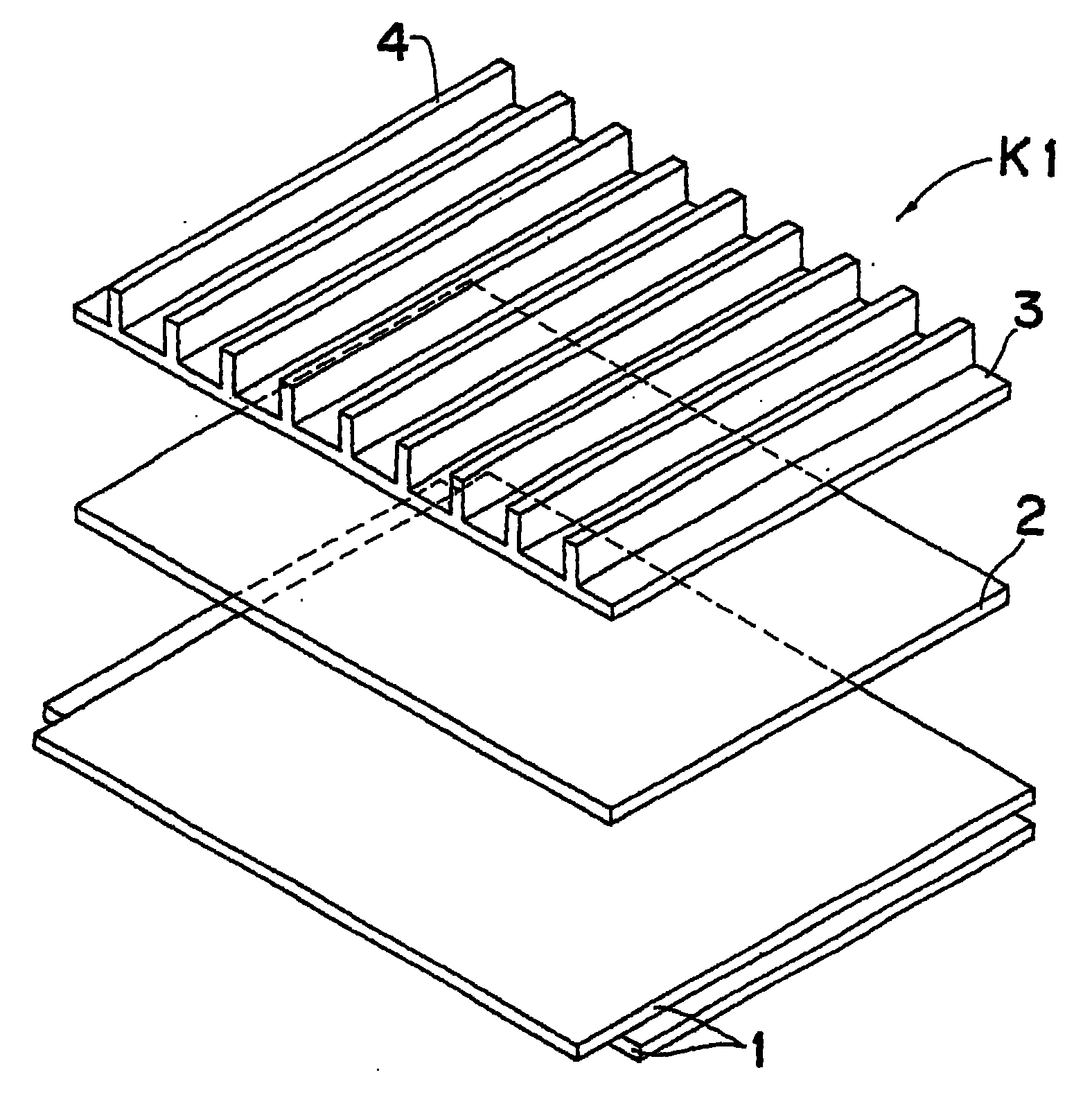
Referring to accompanying drawing, Fig. 5 and Fig. 6 represent the plasm display device K1 of first embodiment of the invention below.Plasm display device comprises plasma display panel 1, heat-conducting medium 2 and as the base plate part 3 of thermal component.The bossy body 4 of realizing heat diffusion effectively is assemblied on the base plate part 3.Heat-conducting medium not only is fit to reduce the temperature difference on plasma display panel 1 plane, and by the heat of plasma display panel 1 is sent to base plate part 3 effectively, and is diffused into air from base plate part 3 and has reduced the temperature of plasma display panel 1.Simultaneously, if heat-conducting medium 2 is made of the soft material of gel state, heat-conducting medium 2 also can be used as buffer medium, prevents the collision from the article on plasma body display panel 1 of outside.
In the present embodiment, with the plasma display panel of 26 inches types as plasma display panel 1.The thickness of heat-conducting medium 2 is 1 to 5mm and is made of the silicon layer of gel state, then the base plate part 3 of aluminum is attached to the whole back side of plasma display panel 1.When realizing that white shows on at plasma display panel 1 whole of the electric energy of 120W, and heat-conducting medium 2 is not compared with the situation that base plate part 3 is attached to plasma display panel 1, the temperature of plasma display panel 1 has descended 25 ℃ approximately.Available rubber layer replaces silicon layer to constitute heat-conducting medium 2.
Simultaneously, because plasma display panel 1 and base plate part 3 have slight bending, so preferably make heat-conducting medium 2 that higher pliability is arranged, so that heat-conducting medium 2 is brought in the plasma display panel 1 and base plate part 3 of airtight connection, thereby not only improved the heat conduction of plasma display panel 1 to base plate part 3, and utilize heat-conducting medium to make plasma display panel 1 prevent magnetic from the outside, in order to reduce the temperature difference and the temperature that reduces plasma display panel 1 on plasma display panel 1 plane effectively, heat-conducting medium 2 preferably has higher conductive coefficient., if constitute heat-conducting medium 2 with the material that high thermal conductivity coefficient is arranged, the tenor in the material just becomes big so, thereby the elasticity of heat-conducting medium 2 and pliability are descended.Therefore, in the plasma display system of second embodiment of the invention shown in Figure 7, heat-conducting medium 2 has the two-layer structure that comprises first and second media 6 and 7.First medium 6 is made of metal level with high thermal conductivity coefficient or carbon-coating, and simultaneously second medium 7 is by the soft silicon layer of gel state or there is the same material of standard conductive coefficient to constitute.By the thickness of first medium 6 is reduced to 0.1 to 0.5mm, can make first medium 6 possess pliability.Utilize first medium 6, the temperature difference on this display panel of plasma 1 plane that can reduce to cause by the heat that plasma display panel 1 produces.Effectively utilize second medium 7 heat that transmits on first medium 6 is sent to base plate part 3, from base plate part 3, be diffused in the air then.Simultaneously, because heat-conducting medium 2 is flexible, utilize heat-conducting medium 2 can alleviate the vibration and the collision from the outside of plasma display panel 1 therebetween, so that preventing plasma display panel 1 effectively breaks, and guarantee heat-conducting medium 2 and plasma display panel 1 and 3 airtight connections of base plate part, and carry out the heat conduction of 1 pair of base plate part 3 of plasma display panel effectively.
Among the plasm display device K2, it is that 800 to 1000W/m ℃, thickness are 0.1 to 0.5mm carbon-coating that first medium 6 adopts conductive coefficients, and second medium 7 adopts the silicon of gel states simultaneously, and its conductive coefficient is that 1 to 5W/m ℃, thickness are 1 to 5mm.Utilize this heat-conducting medium 2, can show as shown in Figure 4 be the image of the middle body at the end with the black background for bright image.At this moment, the temperature distributing characteristic of the plasma display panel 1 of the plasm display device K2 of the 8 expression X-X along the line (Fig. 4) of the solid line among Fig. 8.On the other hand, the temperature distributing characteristic of the plasma display panel 1 of the plasm display device K1 of 9 expressions of the dotted line among Fig. 8 X-X along the line.Compare with the temperature distributing characteristic of the plasm display device K1 of dotted line 9 expression, the temperature distributing characteristic of the plasm display device K2 of solid line 8 expressions spreads the middle body of the heat on plasma display panel 1 plane from plasma display panel 1 more fully to each limit part of plasma display panel 1.As a result, compare, show the temperature difference on plasma display panel 1 plane that has reduced plasm display device K2 with the situation of plasm display device K1.This is because of the conductive coefficient that has 800 to 1000W/m ℃ as the carbon-coating of first medium 6 on its surface direction.Though be lower than conductive coefficient on its surface direction at the carbon-coating conductive coefficient on its thickness direction as first medium 6, but utilize thin carbon layer as constituted above, on thickness direction, still can from plasma display panel 1, be sent to heat effectively on the base plate part 3.
Among plasm display device K1 and the K2, as what from the line 8 of Fig. 8 and line 9, obviously see, because the temperature difference on plasma display panel 1 plane is less than 20 ℃, so can prevent breaking of plasma display panel 1.
Available Copper Foil, aluminium foil or analog replace carbon-coating to constitute first medium 6, and simultaneously available rubber replaces silicon layer to constitute second medium 7.
Clearly indicated among the present invention first and second embodiment just as described above, because heat-conducting medium is arranged between plasma display panel and the base plate part, so not only reduced the temperature of work ionic medium body display panel, and reduced temperature difference on the plasma display panel plane, thereby can obtain highly reliable plasm display device.In addition,,, saved the electric energy that drives the draft fan motor so eliminated the noise of draft fan motor owing to do not adopt original essential draft fan, and the space that does not need to install the draft fan motor.
Fig. 9 represents the plasm display device K3 of third embodiment of the invention.Among the plasm display device K3, groove 13 is formed on the rectangular edges of base plate part 3, and buffer medium 14 is filled in the groove 13.Heat-conducting medium 2 is arranged on by in buffer medium 14 enclosed areas, so that buffer medium 14 is brought in the heat-conducting medium 2 of airtight substantially connection.
Below, the manufacture method of plasm display device K3 is described.As shown in figure 10, groove 13 is formed on base plate part 3 rectangular edges, and is 5.5mm such as making its width W, depth H is 2mm.To there be rectangular-shaped buffer medium 14 as shown in figure 11 to be filled in this groove 13, thereby as Figure 12 and the buffer medium 14 sealing predetermined zone of utilizing shown in Figure 13.For example, the width of buffer medium 14 is 5mm, highly is 4mm.
Then, as shown in figure 14, silicon resin glue is injected the zone that is surrounded by buffer medium 14 as heat-conducting medium 2, solidify then.At this moment, elevated temperature under normal pressure such as rising to 120 ℃, solidified silicones about 20 minutes, made it become solid-state heat-conducting medium 2.In this case, buffer medium 14 can possess thermal endurance.Silicon resin glue can be dry at normal temperatures, but the solidification of silicon resin glue needs the long time cycle at normal temperatures.
Thickness by solidifying the solid-state heat-conducting medium 2 that aforesaid liquid silicone resin glue obtains is 2mm.By heat-conducting medium 2 is attached on the plasma display panel 1, obtain plasm display device K3.
Available silicon ribbon constitutes buffer medium 14.In this case, after having cured liquid heat-conducting medium, can from base plate part 3, remove this band or just peelable when it is not removed from base plate part 3.In addition, in this case, groove 13 can constitute on base plate part 3.
Simultaneously, replace buffer unit 14, the recess that receives heat-conducting medium 2 can be formed on the face of base plate part 3,, or can only be arranged on the framework that stops the liquid heat-conducting medium outflow on the face of base plate part 3 this face additional guide thermal medium 2.
In the manufacture method of above-mentioned plasm display device K3, because foam infiltrates between heat-conducting medium 2 and base plate part, so can obtain to have the plasm display device K3 of thermal conductive resin and thermal diffusivity.
Figure 15 represents the plasm display device K4 of fourth embodiment of the invention.Be noted that plasm display device K4 is identical with plasm display device K1.Among the plasm display device K4, heat-conducting medium 2 is arranged on the base plate part 3, and plasma display panel 1 is arranged to and close being connected of 2 one-tenth basic envelopes of heat-conducting medium.
Below, the manufacture method of plasm display device K4 is described.Rectangular ring frame mold 16 shown in Figure 17 is fixed on the base plate part shown in Figure 16 3, causes the zone that seals by frame mold 16 shown in Figure 18 and 19.For example, the width of frame mold 16 is 5mm, highly is 2mm.Then, as shown in figure 20, the colloid of heat-conducting medium 2 is penetrated in the zone that is sealed by frame mold 16, be cured then, obtain solid-state heat-conducting medium 2.At this moment, the width of heat-conducting medium 2 is 1 to 5mm, is preferably about 2mm.Afterwards, from base plate part 3, unload frame mold 16, and heat-conducting medium 2 is attached on the plasma display panel 1.As a result, obtain plasm display device K1.
In the manufacture method of plasm display device K4, owing to foam does not infiltrate between heat-conducting medium 2 and base plate part 3, so can obtain to have thermal conductive resin and thermal diffusivity plasma device K4.
Simultaneously, more than among Shuo Ming third and fourth embodiment of the present invention, heat-conducting medium 2 can be made of the flexible material of gel state, so that also can be heat-conducting medium 2 as buffer medium, makes plasma display panel 1 can prevent collision from the outside.
Spelt out among third and fourth embodiment of the present invention just as described above, because heat-conducting medium is arranged between plasma display panel and the base plate part, so reduced the temperature of work ionic medium body display panel, therefore can obtain the plasm display device of high reliability.In addition, in the manufacture method of the plasm display device of third and fourth embodiment of the present invention, can obtain to have the plasm display device of thermal conductive resin and thermal diffusivity, strengthen heat-conducting medium in this method and be connected with plasma display panel and the airtight of base plate part.
Figure 21 represents the plasm display device K5 of fifth embodiment of the invention.Plasm display device K5 comprises casing 22 and the internal structure 36 that is contained in the casing 22.By front housing 24 and back cabinet are assembled formation casing 22 mutually.Many ventilation holes 28 and 30 are respectively formed on the side direction shown in the front housing 24 top and the bottom arrow a, and the light transmission part 32 that glass or analog are made is arranged on the front of front housing 24.In addition, on the side direction of back cabinet 26 top and the bottom, form many ventilation holes 28 and 30.
Internal structure 36 comprises base plate part 38, with L shaped gusset 40 the full display panel 42 of plasma is contained on the front 56 of base plate part 38, constituted and be inserted in the heat-conducting medium 44 between base plate part 38 and the plasma display panel 42 and be bearing in a plurality of circuit boards 46 on the back side 50 of base plate part 38 by silicon chip or analog.In order to send the heat of plasma display panel 42 to base plate part 38 effectively, be provided with heat-conducting medium 44.Simultaneously, in order to encourage and control the light emission of plasma display panel 42, be provided with circuit board 46.
Form plasma display panel 42 with header board and back plate.As seeing on Fig. 5, header board has than the horizontal edge of back plate length and the longitudinal edge shorter than back plate, and therefore, header board and back plate have mutual non-overlapping portions.Although do not mark especially in the drawings, the terminal that is connected with electrode on the plasma display panel 42 is formed in these underlapped parts of front and rear panel.The many film wire (not shown) that respectively carry the former connector at its end are connected on the terminal of welding.The former connector is connected to (not shown) on the formpiston connector that is located on circuit board 46 each limit.Therefore, each circuit board 46 is electrically connected plasma display panel 42.
Make base plate part 38 with the aluminium casting.As shown in figure 22, many fin 52 of heat transmission form with base plate part 38 mold pressing integratedly on the whole zone at the back side 50 that equals base plate part 38 substantially.The fin 52 of each rectangular shape stretches out from the back side 50 of base plate part 38, and vertical extent in parallel to each other, so that laterally keep predetermined each other interval.The present invention uses the experiment of carrying out in this respect and shows: when the width of each fin 52 be gap between about 3mm, the fin 52 be made as about 3mm, during similarly by at interval about 6mm arrangement fin 52, the radiating efficiency of fin 52 is good.But, must be pointed out that fin 52 is not limited to these sizes.In addition, fin 52 also is not limited to above-mentioned shape, also can vertically be divided into mass part.
As shown in figure 22, the fin 52 on the middle section 54 on the back side 50 of base plate part 38 stretches out from the back side 50, because underlying cause is higher than the fin 52 on the retaining zone at base plate 38 back sides 50.That is, by heat is passed to base plate part 38 from plasma panel 42 through heat-conducting medium 44, the temperature of the base plate part 38 that raise.; because the temperature distributing disproportionation of base plate part 38 is even; and it is higher to the upper temp of base plate part 38; the temperature that is higher than base plate part 38 retaining parts; therefore; according to this discovery, should make the radiating efficiency of the radiating efficiency of middle section 54 on the back side 50 of base plate part 38 greater than the retaining zone at base plate part 38 back sides 50.
As shown in figure 21, circuit board 46 is arranged in base plate part 38 back sides last middle section 54 around.Thus, because middle section 54 is not covered by circuit board 46 on the back side 50 of base plate part 38, so the high cooling efficiency of the fin 52 on the middle section just is not subjected to the obstruction of circuit board 46 on the back side 50 of base plate part 38.Simultaneously, support circuit board 46 with the bolt (not shown) that from the back side 50 of base plate part 38, stretches out, and separate, thereby directly do not contact with fin 52 with the end of each fin 52 and the back side 50 of base plate part 38, also directly do not contact the back side 50 of base plate part 38, as shown in figure 23.
On the other hand, a plurality of screw seats 58 that are threaded the hole separately stretch out simultaneously from the periphery of the front 56 of base plate part 38.Because screw seat 58 is suppress simultaneously with base plate part 38 in advance, thus with by welding, flange etc. situation about being compressed on the base plate part 38 behind the screw seat 58 is compared, the quantity that can reduce procedure of processing with reduce cost.
Shown in Figure 21 and 23, gusset 40 is separately positioned on four limits of rectangle plasma display panel 42, is fixed on the base plate part 38 so that the bolt hole that plasma display panel 42 and heat-conducting medium 44 penetrate gusset 40 by screw 60 enters the screwed hole of screw seat 58.Constitute each gusset 40 with mutually orthogonal substantially crossing plate portion 40a and 40b.By the buffer unit made from foamed material 62,, plasma display panel 42 is fixed on the front 56 of base plate part 38 through heat-conducting medium 44 the peripheral crimping of plate part 40a and plasma display panel 42 fronts.
Simultaneously, the plate part 40b of gusset 40 extends along each surface of four outer periphery surfaces 64.The circuit board 46 that is electrically connected and the many above-mentioned film wire of plasma display panel 42 are between the outer periphery surface 64 of plate part 40b and base plate part 38.Therefore, when the internal structure 36 that assembles was installed in the edge of the internal structure 36 that the operator assembles by chucking on back cabinet 26, plate part 40b was used for the protective film lead, makes film wire injury-free.
Among the plasm display device K5 of above-mentioned assembling, when the light emission by plasma display panel 42 showed, the heat that is produced by discharging in the plasma display panel 42 had improved the temperature of plasma display panel 42.By heat-conducting medium 44, the heat that produces on the plasma display panel 42 is sent on the base plate part 38, and from the fin 52 of base plate part 38 integral dies on dissipate effectively.Because the air that this thermal diffusion is heated in casing 22 discharges from the overdraught hole 28 of casing 22, simultaneously, its temperature is that the air of room temperature flows into from the leg space ventilation hole 30 of casing 22.Utilize this free convection, cooling plasma display panel 42 and circuit board 46.Suppose that the highest indoor temperature is 40 ℃, shows in the experiment that this direction is carried out according to the inventor: the temperature in the casing 22 can remain on the maximum temperature that is no more than permission, it equal 40 ℃ add room temperature and.
Because fin 52 is base plate part 38 integral dies with supporting plasma display panel 42, base plate part 38 also be can be used as above-mentioned thermal component, so can obtain the cooling construction of nature, air in this structure in the casing 22 provides free convection, thus the inside of cooling casing 22.Therefore, force to discharge in the casing 22 air and force to cool off the draft fan 52 of casing 22 inside owing to not needing to be provided with, thus the dust suction problem that causes such as noise, draft fan fault and forced ventilation can be eliminated, and can reduce production costs.
Simultaneously, among the plasm display device K5, adopted optional cooling construction as above-mentioned cancellation draft fan., among the plasm display device K5, also draft fan can be set, replenish, to promote the air flows in the casing 22 as a kind of of natural convection air.In this case, compare with the plasm display device of prior art, owing to can reduce the quantity of illustrated draft fan, so can alleviate the above-mentioned defective of the plasm display device of prior art.
Figure 24 represents to improve the plasm display device K5 ' of plasm display device K5.Among the plasm display device K5 ', again auxiliary heat proliferation part 65 is set in place on the fin 52 of middle body 54 on the back side 50 of base plate part 38, thereby further improves the thermal diffusion efficient of the fin 52 on the last middle section 54 of base plate part 38.Become the metallic plate 65a of U-shaped structure and have the sheet metal components 65b grid figure and that be fixed on the inside of metallic plate 65a to constitute auxiliary heat proliferation part 65 by general curved.The air white region 66 of many pros is limited in the auxiliary heat proliferation part 65, thereby extends vertically as fin 52 by identical mode.Each dummy section 66 is not limited to square shape, also can be any other shape.The experiment that the application's inventor carries out in this respect shows: if be provided with auxiliary heat proliferation part 65, compare with the situation that auxiliary heat proliferation part 65 is not set, the temperature of base plate part 38 also can further descend 10 ℃.Therefore, just adopt the plasm display device of DC type plasma display panel, because the heat that produces on the DC plasma display panel is greater than the heat of AC type plasma type display panel, so be particularly suitable for additionally being provided with auxiliary heat proliferation part 65.
Simultaneously, among Figure 24, auxiliary heat proliferation part 65 is set in place on the fin 52 on the last middle section 54 at base plate part 38 back sides 50.; can also arrange fin like this; promptly the fin 52 on the retaining zone of being arranged at the fin 52 on the middle section on the back side 50 of base plate part 38 with base plate part 38 back sides 50 there is the height that equates; promptly; all fin 52 on the back side 50 of base plate part 38 have identical height; then auxiliary heat proliferation part 65 is located at and is positioned on the base plate part 38 on the fin on the middle section 54 52, thereby improve the thermal diffusion efficient of the fin 52 on the last middle section 54 at the back side 50 of base plate part 38.
As what from the above explanation of fifth embodiment of the invention, spell out,, can effectively heat be diffused on the base plate part from plasma display panel by fin and base plate part mold pressing integrally.Because the air in the casing of this thermal diffusion heating discharges from the ventilation hole on casing top, and the air of ambient temperature flows into from the ventilation hole of casing bottom, produces the cross-ventilation of nature.Therefore, cooled off plasma display panel and circuit board, the temperature in the casing can remain under the condition of the maximum temperature that is no more than permission.
Owing to also can adopt the optional cooling construction that cools off casing inside by natural convection air, so do not need to dispose draft fan with the base plate part of supporting plasma display panel as the thermal diffusion plate that high thermal diffusion efficient is arranged.Therefore, can alleviate such as noise, draft fan fault and forced ventilation and cause defectives such as inhaling ash, and can reduce production costs.Simultaneously, when draft fan during as the aid of natural convection air, is compared with the plasm display device of prior art, can reduce the quantity of illustrated draft fan, thereby can eliminate the above-mentioned defective of the plasm display device of prior art, and can reduce production costs.
Figure 25 represents the plasm display device K6 of sixth embodiment of the invention.According to the mode that is same as plasm display device K5, plasm display device K6 comprises casing 22 and internal structure 36.Constitute the heat-conducting medium 44 of internal structure 36 by having thin-layer tablet that thermal conductive resin and flexible material make, such as constituting heat-conducting medium with silicones, and not only it is used for effectively the heat that produces on the plasma display panel 42 being passed to base plate part 38, but also can be used as buffer medium.As shown in figure 26, heat-conducting medium 44 has the size that is substantially equal to plasma display panel 42.Simultaneously, utilize in the grid figure without any arranging a plurality of synusia 70 with gap, formation heat-conducting medium 44.
Figure 26 and 27 presentation surface article on plasma body display panel 42 and base plate part 38 respectively has the thin slice 70 of opposing face 70A and 70B.On the face 70A of thin slice 70, constitute a plurality of protuberances 74, grid groove 72 is limited between the protuberance 74 by matrix shape.Thin slice 70 is a square, and its length of side is 100mm, and thickness is 2mm.Protuberance 74 is square, and length is 13mm, highly is 1mm, and the width W of groove 72 is 2mm simultaneously., these shape and size are unrestricted, also can carry out various changes.
As shown in figure 28, plasma display panel 42 is assembled with base plate part 38.At first, four sections two-sided tapes 78 that thickness is equated with heat-conducting medium 44 substantially are attached to respectively on four neighborings of base plate part 38 fronts 56.Then, the heat-conducting medium 44 of the heat conduction that is made of the good thin slice 70 of arrangement is placed on the front 56 of base plate part 38, makes the face 70A of each thin slice 70, promptly the protuberance 74 of each thin slice 70 is towards plasma display panel 42.Then, utilize roll or analog, extrude the air between base plate part 38 and the heat-conducting medium 44 fully, make heat-conducting medium 44 form sealing and contact with base plate part 38.Because the reverse side toughness of heat-conducting medium 44, so, between base plate part 38 and heat-conducting medium 44, just can not infiltrate air in case heat-conducting medium 44 forms sealing with base plate part 38 contacts.
Then, plasma display panel 42 is placed on two-sided tape 78 and the heat-conducting medium 44, and with hand from top two-sided tape 78 and the heat-conducting medium 44 of flattening gently.As a result, each protuberance 74 of the thin slice 70 of plasma display panel 42 and heat-conducting medium 44 formed to compress contact, square protuberance 74 is flattened and lateral expansion.Each groove 72 of thin slice 70 is as the outside exhaust in exhaust passage between this phase of expansion of protuberance 74, and the protuberance 74 that finally is inflated ties up and disappears.Therefore, owing to eliminated the air layer between heat-conducting medium 44 and the plasma display panel 42 substantially fully, 42 mutual formation sealings contact so that heat-conducting medium 44 is with plasma display panel in institute, and utilize two-sided tape 78 that plasma display panel 42 is fixed on the base plate part 38.Because plasma display panel 42 is not transparent, so can not observe exhaust process., it can confirm by experiment, promptly compresses when contact when transparent glass plate and heat-conducting medium 44 form, and glass plate does not have the sealing of air layer formation to contact with heat-conducting medium 44 therebetween with regard to being formed on.
Simultaneously, when plasma display panel 42 has compressed heat-conducting medium 44, even air layer is retained in the groove 72, plasma display panel 42 as a whole also can contact with heat-conducting medium 44 substantially equably, therefore, air layer is retained between heat-conducting medium 44 and the plasma display panel 42 substantially equably.Therefore, compare, improved thermal conductivity, and to make thermal conductivity be uniform in the whole zone of plasma display panel 42 with the situation that air layer is retained between heat-conducting medium 44 and the plasma display panel 42 partly.
Among the plasm display device K6, protuberance 74 and groove 72 are provided with on one of them face of heat-conducting medium, and being placed on, plasma display panel 42 flattens gently on the back side of heat-conducting medium 44 and back to this face, so that discharge the air that exists between aforesaid heat-conducting medium 44 and the plasma display panel 42.Therefore, contacting because heat-conducting medium 44 and plasma display panel 42 can easily form sealing mutually, is uniform so can make the thermal conductivity on the whole zone of plasma display panel 42.
Figure 29 and 30 expressions improve the thin slice 70a of the thin slice 70 of Figure 26.Among the thin slice 70a, arranging a plurality of circular bulge 74a, so that form mutual contact.As shown in figure 30, each protuberance 74a has the convex surface, and its thickness is reduced to its outward flange gradually from its middle body.There is not the protuberance 74a of protuberance 74a and the interface 80 between the regional 72a groove 72 corresponding to synusia 70.Thin slice 70a can obtain the effect identical with thin slice 70.
Simultaneously, the thin slice 70b of Figure 31 and another improvement thin slice 70 of 32 expressions.Thin slice 70b has the convex surface, and its thickness is reduced to its outward flange gradually from its middle body.Therefore, when constituting heat-conducting medium 44 by assembled laminae 70b, the middle body of thin slice 70b is just as the protuberance 74 of thin slice 70, and the outward flange of thin slice 70b is just as the groove 72 of thin slice 70 simultaneously.Therefore, the heat-conducting medium 44 that is made of thin slice 70b can obtain the effect identical with the heat-conducting medium that constitutes with thin slice 70 44.
Protuberance 74 and groove 72 can be formed on one of them face of heat-conducting medium 44, also can be formed on the reverse side of heat-conducting medium 44.Simultaneously, can constitute heat-conducting medium 44, also can and produce protuberance 74 respectively and the protuberance of the effect of groove 72 and the single sheet of groove constitute it by the size that equals plasma display panel 42 substantially by arranging a plurality of thin slices 70,70a or 70b.
Spelt out in the above-mentioned explanation as sixth embodiment of the invention, protuberance and groove are arranged on one of them face of heat-conducting medium, plasma display panel is placed on the heat-conducting medium face, and be used for flattening the heat-conducting medium back side gently, so that discharge the air that retains between heat-conducting medium and the plasma display panel.Therefore, in the sixth embodiment of the invention, owing to do not stockpiling between plasma display panel and the heat-conducting medium under the situation of a large amount of air, plasma display panel can easily form sealing mutually with heat-conducting medium and contact, so on the whole zone of plasma display panel, it is uniform can making thermal conductivity.