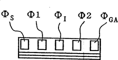
Use the light pen of self-scanned luminescent array
Technical field
The present invention relates to light pen, particularly relate to the light pen that uses self-scanned luminescent array.
Background technology
Optical printer head is a light pen, possesses the light-emitting element array that makes luminescent device be arranged in row and constitute.As light-emitting element array, for example using light-emitting diode (LED) array to constitute under the situation of optical printer head, when printing the light pen of 600dpi (dots perinch, dots per inch) on the printing paper of A3 size, row approximately will be arranged 7200 LED.Under the situation of such light pen, all want extraction electrode from each LED, and be electrically connected with the electrode of drive IC.Connect and to use the gold wire bonding technology usually.Usually, drive the IC of n LED, go here and there-and conversion, so that n serial data is transformed into n parallel data, turn off the light according to the bright lamp of n LED of this parallel data control.
Therefore, the bar number of the holding wire that light pen takes out, if remove power supply with for the holding wire of regularly relevant pulse use outside, equate with the bar number of drive IC.But, if like this then under the too much situation of the bar number of holding wire, adopt the way of data allocations being given the specific drive IC of m drive IC (go here and there-and conversion) is set, just can reduce to 1/m to the bar number of the holding wire that will take out.
As mentioned above, use the existing light pen of led array, owing to have the wiring of LED number just, thus if need not go here and there near the above-mentioned specific drive IC-and the bar number of the conversion minimizing holding wire that will take out, then become for can not form and the outside between the structure of interface.For this reason, because of the result becomes to will disposing specific drive IC in the same substrate top with led array, so exist the problem that the width (with the meet at right angles width of direction of the orientation of LED) of light pen broadens.And, owing to will go here and there-also the special-purpose specific drive IC of conversion is built in the write head, has increased cost.
On the other hand, the inventor, about inscape as light-emitting element array, the thyristor of concentrating on to have the pnpn structure, can realize this situation of self-scanning of luminous point, (spy opens flat 1-238962 communique to have proposed patent application, Te Kaiping 2-14584 communique, Te Kaiping 2-92650 communique, spy open flat 2-92651 communique), shown as optical printer can form carefully, can make light-emitting element array of small compact or the like in pitch easy aspect the installation, luminescent device with light source.
In addition, the inventor etc. have also proposed the scheme (Te Kaiping-No. 263668 communique) of self-scanned luminescent array, its structure be the carrying device that constitutes by luminous thyristor as shift register, separate with light-emitting element array.
Summary of the invention
The objective of the invention is to, provide the way that can adopt self-scanned luminescent array to reduce the light pen of the bar number of the holding wire that will take out.
To achieve these goals, the invention provides a kind of light pen, arranging a plurality of self-scanned luminescent array chips, comprising with the one dimension state:
1 dimension ground arrange the gate electrode with control threshold voltage or threshold current a plurality of 3 end carrying devices, the gate electrode of adjacent carrying device is connected to each other, by each load resistance power line is connected on each gate electrode of above-mentioned carrying device, n phase clock impulse line is connected to the carrying device array that forms on the negative electrode of above-mentioned each carrying device or the anode with the interval of n carrying device respectively with having electric unidirectional device by the electric current limiting resistance; Said n is the integer more than or equal to 2;
3 gate electrode identical with quantity above-mentioned carrying device end luminescent devices with control threshold voltage or threshold current are arranged with 1 dimension state, each gate electrode of above-mentioned luminescent device is connected on the gate electrode of correspondence of every n above-mentioned carrying device, and the line that adds write signal is connected to the light-emitting element array that forms on the negative electrode of above-mentioned each luminescent device or the anode by the electric current limiting resistance;
It is one group a plurality of groups that above-mentioned a plurality of chip is divided into m chip, and on all chips in each group, independent initial pulse bus and above-mentioned 1 is tieed up the gate electrode that is in the carrying device of original position in the carrying device of arrangement and is connected; Above-mentioned m is the integer more than or equal to 1;
The m bar clock pulse bus of certain phase is connected on m the interior chip of each group with the interval of m chip respectively;
The clock pulse bus of other common phases is connected on each chip;
Common write signal bus is connected on each chip.
In addition, light pen of the present invention is being arranged a plurality of self-scanned luminescent array chips with the one dimension state, comprising:
1 dimension ground arrange the gate electrode with control threshold voltage or threshold current a plurality of 3 end carrying devices, the gate electrode of adjacent carrying device is connected to each other, by each load resistance power line is connected on each gate electrode of above-mentioned carrying device, n phase clock impulse line is connected to the carrying device array that forms on the negative electrode of above-mentioned each carrying device or the anode with the interval of n carrying device respectively with having electric unidirectional device; Said n is the integer more than or equal to 2;
Make 3 gate electrode identical end luminescent devices arrange, each gate electrode of above-mentioned carrying device is connected to 1 dimension state on the corresponding gate electrode of above-mentioned luminescent device, the line that adds write signal is connected on the negative electrode of above-mentioned each luminescent device or the anode and the light-emitting element array of formation with quantity above-mentioned carrying device with control threshold voltage or threshold current;
In each chip, common initial pulse bus and above-mentioned 1 is tieed up the gate electrode that is in the carrying device of original position in the carrying device of arranging and is connected;
Common n phase clock pulse bus is connected on each chip;
2 independent write signal buses are connected on each chip, and above-mentioned 2 write signal buses whenever are connected on the above-mentioned luminescent device in each chip alternately.
In addition, light pen of the present invention is being arranged a plurality of self-scanned luminescent array chips with the one dimension state, comprising:
1 dimension ground arrange the gate electrode with control threshold voltage or threshold current a plurality of 3 end carrying devices, the gate electrode of adjacent carrying device is connected to each other, by each load resistance power line is connected on each gate electrode of above-mentioned carrying device, n phase clock impulse line is connected to the carrying device array that forms on the negative electrode of above-mentioned each carrying device or the anode with the interval of n carrying device respectively with having electric unidirectional device by the electric current limiting resistance; Said n is the integer more than or equal to 2;
The line that 3 gate electrode identical with quantity above-mentioned carrying device end luminescent devices with control threshold voltage or threshold current are arranged, each gate electrode of above-mentioned luminescent device is connected to 1 dimension state on the corresponding gate electrode of the individual above-mentioned carrying device of every n, adds write signal by electric current limiting resistance handle is connected to the light-emitting element array that forms on the negative electrode of above-mentioned each luminescent device or the anode;
In each chip, independent initial pulse bus respectively with carrying device that above-mentioned 1 dimension is arranged in be in the carrying device of original position gate electrode be connected;
Common n phase clock pulse bus is connected on each chip;
Common write signal bus is connected on each chip.
In addition, light pen of the present invention is being arranged a plurality of self-scanned luminescent array chips with the one dimension state, comprising:
1 dimension ground arrange the gate electrode with control threshold voltage or threshold current a plurality of 3 end carrying devices, the gate electrode of adjacent carrying device is connected to each other, by each load resistance power line is connected on each gate electrode of above-mentioned carrying device, n phase clock impulse line is connected to the carrying device array that forms on the negative electrode of above-mentioned each carrying device or the anode with the interval of n carrying device respectively with having electric unidirectional device; Said n is the integer more than or equal to 2;
Make 3 gate electrode identical end luminescent devices arrange, each gate electrode of above-mentioned carrying device is connected to 1 dimension state on the corresponding gate electrode of above-mentioned luminescent device, the line that adds write signal is connected on the negative electrode of above-mentioned each luminescent device or the anode and the light-emitting element array of formation with quantity above-mentioned carrying device with control threshold voltage or threshold current;
M bar initial pulse bus is connected on the gate electrode of the carrying device that is in original position in the carrying device that above-mentioned 1 dimension of relevant chip arranges with the interval of m chip respectively; Above-mentioned m is the integer more than or equal to 2;
Common n phase clock pulse bus is connected on each chip;
It is one group a plurality of groups that above-mentioned a plurality of chip is divided into a m adjacent one another are chip, and independent write signal bus is connected respectively on all chips in each chipset;
The resistor that is connected on above-mentioned initial pulse bus, n phase clock pulse bus, the write signal bus is built in the chip.
In addition, light pen of the present invention is being arranged a plurality of self-scanned luminescent array chips with the one dimension state, comprising:
1 dimension ground arrange the gate electrode with control threshold voltage or threshold current a plurality of 3 end carrying devices, the gate electrode of adjacent carrying device is connected to each other, by each load resistance power line is connected on each gate electrode of above-mentioned carrying device, n phase clock impulse line is connected to the carrying device array that forms on the negative electrode of above-mentioned each carrying device or the anode with the interval of n carrying device respectively with having electric unidirectional device; Said n is the integer more than or equal to 2;
Make 3 gate electrode identical end luminescent devices arrange, each gate electrode of above-mentioned carrying device is connected to 1 dimension state on the corresponding gate electrode of above-mentioned luminescent device, the line that adds write signal is connected on the negative electrode of above-mentioned each luminescent device or the anode and the light-emitting element array of formation with quantity above-mentioned carrying device with control threshold voltage or threshold current;
It is one group a plurality of groups that above-mentioned a plurality of chip is divided into a m adjacent one another are chip; Above-mentioned m is the integer more than or equal to 2;
In the chip in one group, the gate electrode of last carrying device of chip is connected with the gate electrode of the initial carrying device of adjacent next chip by electric unidirectional device;
In the initial chip in each group, common initial pulse bus is connected above-mentioned 1 and ties up on the gate electrode of the carrying device that is in original position in the carrying device of arranging;
Common n phase clock pulse bus is connected on each chip;
Independent write signal bus is connected on all interior chips of each chipset.
In addition, light pen of the present invention is being arranged a plurality of self-scanned luminescent array chips with the one dimension state, comprising:
1 dimension ground arrange the gate electrode with control threshold voltage or threshold current a plurality of 3 end carrying devices, the gate electrode of adjacent carrying device is connected to each other, by each load resistance power line is connected on each gate electrode of above-mentioned carrying device, n phase clock impulse line is connected to the carrying device array that forms on the negative electrode of above-mentioned each carrying device or the anode with the interval of n carrying device respectively with having electric unidirectional device; Said n is the integer more than or equal to 2;
Make 3 gate electrode identical end luminescent devices arrange, each gate electrode of above-mentioned carrying device is connected to 1 dimension state on the corresponding gate electrode of above-mentioned luminescent device, the line that adds write signal is connected on the negative electrode of above-mentioned each luminescent device or the anode and the light-emitting element array of formation with quantity above-mentioned carrying device with control threshold voltage or threshold current;
It is one group a plurality of groups that above-mentioned a plurality of chip is divided into a m adjacent one another are chip, and on all chips in each group, independent initial pulse bus and above-mentioned 1 is tieed up the gate electrode that is in the carrying device of original position in the carrying device of arrangement and is connected; Above-mentioned m is the integer more than or equal to 2;
The m bar clock pulse bus of a certain phase is connected on m the interior chip of each group with the interval of m chip respectively;
The clock pulse bus of other common phases is connected on each chip;
Common write signal bus is connected on each chip.
The 1 self-scanned luminescent array chip of lighting the lamp type that can use in light pen of the present invention has following such essential structure.
In other words, one lights the self-scanned luminescent array chip of lamp type, comprising:
1 dimension ground arrange the gate electrode with control threshold voltage or threshold current a plurality of 3 end carrying devices, with have electric unidirectional device make the gate electrode of adjacent carrying device be connected to each other, power line be connected on each gate electrode of carrying device by each load resistance, n phase (n for more than or equal to 2 integer) clock pulse line, be connected to the last formed carrying device array of a side of 2 remaining terminals of each carrying device respectively in order by every phase n carrying device
Make a plurality of 3 end luminescent devices, 1 dimension ground arrange, each gate electrode of carrying device is connected to the last light-emitting element array of formation of a side in 2 the remaining terminals that are connected to each luminescent device on the gate electrode of correspondence of luminescent device, the line that adds write signal with gate electrode of control threshold voltage or threshold current.
The 1st scheme according to light pen of the present invention, then make a plurality of above-mentioned such self-scanned luminescent arrays of lighting the lamp type that constitute, arrange one-dimensionally, common initial pulse bus is connected on each chip, 2 common phase clock pulse buses are connected on each chip, independent write signal bus is connected respectively on each chip.
In addition, if according to the 2nd scheme of light pen of the present invention, then in the 1st scheme, the electric current limiting resistance that is connected on initial pulse bus, n phase clock pulse bus, the write signal bus is built in the chip.
In addition, if according to the 3rd scheme of light pen of the present invention, then in the 1st scheme, the electric current limiting resistance that is connected on the clock pulse bus of n phase is built in the chip.
In addition, if according to the 4th scheme of light pen of the present invention, then the clock pulse bus to each bar n phase all inserts buffer IC in the 3rd scheme.
In addition, according to the 5th scheme of light pen of the present invention, then use the 2 self-scanned luminescent battle array chips of lighting the lamp type.Under the situation of this scheme, common initial pulse bus is connected on each chip, the clock pulse bus of 2 common phases is connected on each chip, 2 independent write signal buses are connected respectively on each chip, in each chip, write pulse bus to above-mentioned 2, be connected on the above-mentioned luminescent device every a ground.In addition, according to the 6th scheme of the present invention, then adopt the self-scanning light-emitting element array of a plurality of bright lamp types.
The self-scanning light-emitting element array chip of these a plurality of bright lamp types comprises:
A plurality of 3 end carrying devices of the gate electrode with control threshold voltage or threshold current are arranged on 1 dimension ground, with having electric unidirectional device the gate electrode of adjacent carrying device is connected to each other, power line is connected on each gate electrode of carrying device by each load resistance, n phase (n is the integer more than or equal to 2) clock pulse line is connected in order the last formed carrying device array of a side of 2 remaining terminals of each carrying device respectively by the electric current limiting resistance by every phase n carrying device
Make a plurality of 3 end luminescent devices, 1 dimension ground arrange, each gate electrode of luminescent device is connected to the light-emitting element array that the side in 2 the remaining terminals that on the gate electrode of correspondence of every n carrying device, by the electric current limiting resistance line that adds write signal are connected to each luminescent device upward forms with gate electrode of control threshold voltage or threshold current.
This self-scanned luminescent array arrangements of chips is become under the situation of light pen of one dimension, respectively independent initial pulse bus is connected on each chip, common n phase clock pulse bus is connected on each chip, common electric current is applied bus be connected on each chip.
In addition, the 7th scheme of the present invention, using one to light in the light pen of self-scanned luminescent array chip of lamp type, repeatedly be connected on each chip in order the initial pulse bus of m bar (m is the integer more than or equal to 2), the clock pulse bus of common n phase is connected on each chip, independent write signal bus is connected respectively on each the chip of adjacent m, is connected to incorporating resistor on initial pulse bus, clock pulse bus, the write signal bus in chip.
In addition, under the situation of the 8th scheme of the present invention, using one to light in the light pen of self-scanned luminescent array chip of lamp type, a plurality of chips, the chipset that is divided into m adjacent one another are (m is the integer more than or equal to 2), in the chip in one group, the terminal point bonding welding pad of a certain chip is connected with the initial pulse bonding welding pad of the chip of next stage, common initial pulse bus is connected on the interior initial chip of each chipset, the clock pulse bus of common n phase is connected on each chip, independent write signal bus is connected respectively on all chips of each chip.
In addition, in the 9th scheme of the present invention, in the light pen of the self-scanned luminescent array chip that uses the bright lamp type of multiple spot, independent initial pulse bus is connected on the individual chip of adjacent every m (m is the integer more than or equal to 2), the clock pulse bus of the m bar of a certain phase is connected on the individual chip of adjacent m in order, the clock pulse bus of common other phase is connected on each chip, the write signal bus is connected respectively on each chip.
Description of drawings
Fig. 1 shows the essential structure of the luminous thyristor of 3 ends.
Fig. 2 is the equivalent circuit diagram of self-scanned luminescent array.
Fig. 3 shows the light pen as embodiments of the invention 1.
Fig. 4 A, Fig. 4 B show in embodiment 1 a SLED chip of lighting the lamp type that uses.
Fig. 5 shows the light pen as embodiments of the invention 2a.
Fig. 6 A, Fig. 6 B show the SLED chip of the incorporating resistor type that uses in embodiment 2a.
Fig. 7 A, Fig. 7 B show the SLED chip of the incorporating resistor type that uses in embodiment 2b.
Fig. 8 shows the light pen as embodiments of the invention 2c.
Fig. 9 shows the light pen as embodiments of the invention 3.
Figure 10 A, Figure 10 B show in embodiment 3 the 2 SLED chips of lighting the lamp type that use.
Figure 11 shows the light pen as embodiments of the invention 4.
Figure 12 shows the SLED chip of the bright lamp type of multiple spot that uses in embodiment 4.
Figure 13 shows the light pen as embodiments of the invention 5.
Figure 14 shows the drive waveforms example of embodiment 5.
Figure 15 shows the light pen as embodiments of the invention 6.
Figure 16 A, Figure 16 B show in embodiment 6 the 1 SLED chip of lighting the lamp type that uses.
Figure 17 shows the drive waveforms example of embodiment 6.
Figure 18 shows the light pen as embodiments of the invention 7.
Embodiment
At first, simply the self-scanned luminescent array that uses light pen of the present invention is described.Self-scanned luminescent array uses the luminous thyristor of 3 ends.In Fig. 1, show the essential structure of the luminous thyristor of 3 ends.As an example, form PNPN structure 12 in P type GaAs substrate 10 tops.The control utmost point 14 of the luminous thyristor of this 3 end has the effect that voltage is connected in control, is added to the connection voltage on the negative electrode 16, will become to the diffusion potential of PN junction and control voltage are added to the voltage of controlling on the pole tension.In addition, after connection, the control pole tension becomes to consistent substantially with anode voltage.Therefore, if anode 18 ground connection is then controlled pole tension and will be become and be 0V.
Fig. 2 show use so luminous thyristor of 3 ends, open the equivalent electric circuit of disclosed self-scanned luminescent array in the flat 2-263668 communique above-mentioned spy.This self-scanned luminescent array possesses carrying device T
1, T
2, T
3... array and write and use luminescent device L
1, L
2, L
3... array.These luminescent devices and carrying device are made of the luminous thyristor of 3 ends, between the gate electrode of adjacent carrying device, use diode D
1, D
2, D
3, D
4Connect.
Each cathode electrode of carrying device is alternatively supplied with clock pulse 1, 2.V
GABe that power supply is (normally-5V), via load resistance R
LBe connected to the gate electrode G of each carrying device
1, G
2, G
3... on.These carrying devices T
1, T
2, T
3..., diode D
1, D
2, D
3..., by means of a plurality of load resistance R
L, constitute shift register 8.The gate electrode of carrying device also is connected on the gate electrode of corresponding luminescent device.Give the carrying device T of the 1st row
1Gate electrode add initial pulse
SAdd write signal for the cathode electrode that writes with luminescent device
I
The action of this self-scanned luminescent array of simple declaration.
Now, suppose carrying device T
2Be in the ON state, gate electrode G
2Voltage, just from supply voltage V
GA(-5V) risen, and becomes to being almost 0.Therefore, if write signal
IVoltage be lower than the diffusion potential (approximately 1V) of PN junction, then can make luminescent device L
0Become and be luminance.
To this, gate electrode G
1Be about-5V gate electrode G
3Become and be pact-1V.Therefore, luminescent device L
1Write voltage become for approximately-6V, luminescent device L
3Write voltage become for approximately-2V.Then, only to luminescent device L
2The write signal that writes
IVoltage will become and be-1 to-2V scope.As luminescent device L
2Become and be ON, when becoming in other words to luminance, write signal
IThe voltage of line is fixed as approximately-1V, does not select other luminescent device and luminous possibility so do not have.
The luminous intensity of luminescent device is by flowing to write signal
IMagnitude of current decision, can carry out image with intensity arbitrarily and write.For luminance being sent to the luminescent device of next, must make write signal in addition
IThe voltage of line temporarily is reduced to 0V, makes just temporarily to become at luminous luminescent device to be OFF.
Under the situation of in such self-scanned luminescent array being applied to optical printer etc., going, form as a semiconductor chip of carrying device that is integrated with a certain some and luminescent device constitutes the self-scanned luminescent array chip, this self-scanned luminescent array chip for example is arranged in row, forms the self-scanned luminescent array of given size.
Below, explain the light pen that uses such linearity light source with reference to the accompanying drawings
Embodiment.
Embodiment 1
As shown in Figure 3, make 56 600dpi/128 luminous point/one light self-scanned luminescent array (the being abbreviated as SLED) arrangements of chips of lamp type (a bright lamp of luminescent device while), constitute A3 size light pen.A SLED chip of lighting the lamp type of Shi Yonging is shown in Fig. 4 A, Fig. 4 B in this embodiment.
SLED shown in Fig. 4 B is by 128 carrying device T
1~T
128With 128 write and use luminescent device L
1~L
128Constitute.Shift register partly constitutes, and the connection between the gate electrode of adjacent carrying device uses diode to connect.V
GABe power supply, via load resistance R
LBe connected on the gate electrode of each carrying device.In addition, the gate electrode of carrying device also is connected on the gate electrode of corresponding luminescent device.Give carrying device T
1Gate electrode add initial pulse
SAlternatively add clock pulse 1, 2 for the cathode electrode of carrying device.Add write signal for the cathode electrode that writes with luminescent device
I
In such SLED chip, shown in Fig. 4 A, have 1, 2, V
GA,
S,
IWith bonding welding pad 30,32,34,36,38.
Get back to Fig. 3, subtend is arranged with the signal routing that 56 self-scanned luminescent arrays with SLED chip of bonding welding pad 30,32,34,36,38 as described above connect up and describes.V from connector 20
GATerminal, 2 terminals, 1 terminal,
STerminal extends a bus 22,24,26,28 respectively. 1 bonding welding pad 30 of each SLED chip is connected on 1 bus 26 by the electric current limiting resistance R1 that adds, and 2 bonding welding pads 32 are connected on 2 buses 24 by the electric current limiting resistance R2 that adds.In addition,
S Bonding welding pad 36 is by the electric current limiting resistance R that adds
SBe connected to
SOn the bus 28, V
GA Bonding welding pad 34 is connected to V
GAOn the bus 22.The of each SLED chip is arranged again
IBonding welding pad 38 is by the electric current limiting resistance R that adds
I, through write signal
I(1)~
I(56) bus of usefulness is connected to the of the correspondence of connector 20
I(1)~
I(56) on the terminal.
Under the situation of such write head, owing to same initial pulse Ф is provided for each SLED chip
SSo, begin to transmit action simultaneously.In each SLED chip just in the luminous intensity of a luminescent device of bright lamp, by the write signal that offers each SLED chip respectively
I(1)~
I(56) decision.
The light pen that below constitutes like that from the wiring number that chip takes out, is given
S, 1, 2, V
GA,
I(1)~
I(56) earthy wiring (not drawing) is added in the wiring of the bonding welding pad of usefulness, adds up to 61.With the wiring ratio of the existing light pen that uses led array, the cloth number of lines become and lack, in addition, employed resistance R 1, R2, R
S, R
ISum, be 56 * 4=224.
In addition, in the above-described embodiment, though that explanation is 2 SLED that drive mutually that drive with clock pulse 1, 2 with transmitting,, also can be the SLED that uses the clock pulse more than or equal to 3 phases to drive.
Embodiment 2a
Present embodiment is impressed current limiting resistance R1, R2, the R the light pen of Fig. 3
S, R
IBe built in the light pen in the SLED chip.
As shown in Figure 5, make 600dpi/128 luminous point/one of 56 built-in resistors light the SLED arrangements of chips of lamp type, constitute A3 size light pen.Fig. 6 A, Fig. 6 B show the SLED that uses in the present embodiment.
Shown in Fig. 6 B, the SLED chip is built-in with electric current limiting resistance R1, R2, R
S, R
IThese resistance are inserted into 1 line 40, 2 lines 42, respectively
S Line 46,
IIn the line 48.The number of the bonding welding pad of a chip as shown in Figure 6A, is the same with embodiment 1.
Just as the write head of the write head that makes Fig. 5 and Fig. 3 compare just can understand, as electric parts, can realize only using the light pen of SLED chip, can realize the light pen that width is narrower.
Embodiment 2b
Present embodiment does not use the SLED chip of embodiment 2a, uses the only SLED chip of built-in current limiting resistance R1, R2 and replace.Fig. 7 A, Fig. 7 B show the SLED chip that uses in the present embodiment.Under the situation of this SLED chip, respectively resistance R 1, R2 are inserted in 1 line 40, 2 lines 42, to
S Line 46,
IDo not insert the electric current limiting resistance in the line 48.As mentioned above, because not to
IInsert resistance in the line 48, so with the of driven with current sources connector 20
I(1)~
I(56) terminal.In addition, voltage between the anode-cathode of the thyristor of ON state equally keeps the forward voltage of PN junction substantially and irrelevant with electric current.Utilize this character, also can use voltage source and resistor group formation altogether as current source.As mentioned above, because not to
IInsert resistance in the line 48, so as shown in Figure 6, owing to having eliminated resistance R
IBe built in the heating that is taken place under the situation in chip or the light pen, so and the chip of Fig. 6 relatively can prevent the rising of chip temperature.
Embodiment 2c
Fig. 8 shows the light pen of present embodiment.In the present embodiment, in the 1 of the light pen of embodiment 2b, 2 buses, inserted buffer IC61,62.
Why insert buffer IC, it be the reasons are as follows.In other words, when flowing into the electric current of about 5mA in each bar line of the of SLED chip 1 line, 2 lines, the electric current that flows to 1 line 26, 2 lines 24 in 60 chips respectively will be up to 300mA.When big electric current carries out can producing undesirable radiation when interrupted, exist the danger of the fault that generates electromagnetic waves.The way of buffer IC is inserted in employing in bus, just can stop the generation because of the interrupted radiation that produces of big electric current.
In addition, adopt the way of inserting buffer IC, as long as the voltage also high or also lower than the threshold value of buffer IC is offered 1, 2 terminals of connector 20.Under the situation of the SLED of carrying device chip with diode-coupled, from operating principle say be difficult to 3V make it the action, but adopt the way of inserting buffer IC,, can drive the SLED chip with the signal of 3V system although need other 5V power supply.So, just can adopt the way that reduces supply voltage to reduce power consumption.
Embodiment 3
Present embodiment is the A3 size light pen that self-scanned luminescent array (the being abbreviated as SLED) arrangements of chips that makes 56 600dpi/128 luminous point/2 light lamp type (2 luminescent device simultaneously bright lamp) gets up to constitute.
Fig. 9 shows the formation of light pen, and Figure 10 A, Figure 10 B show the SLED chip that uses in the present embodiment.
SLED chip shown in Figure 10 A, Figure 10 B is removed the write signal in the SLED chip of Fig. 6
IOutside, also have write signal
JTo
JInsert electric current limiting resistance R in the line 49
JWrite signal
I,
JAlternatively be connected on the luminescent device.By means of this, make in a chip, to make 2 bright lamps of luminescent devices while become possibility, the duty ratio of write signal increases in addition, and the light quantity of validity increases.
If with the light pen of present embodiment, as shown in Figure 9, owing to 2 write signal bus all are provided for each chip
I(1)~
I(56),
J(1)~
J(56), thus with embodiment 1 relatively, increase by 56 buses, becoming from the taking-up total line number of chip taking-up is 117.
In addition, in each chip, the transmission clock bus also can be more than or equal to 3 phases, and the write signal bus also can be more than or equal to 3.
Embodiment 4
Present embodiment is to make the A3 size write head that 56 600dpi/128 luminous points/a plurality of self-scanned luminescent array arrangements of chips of lighting lamp type (a plurality of luminescent devices are bright lamp simultaneously) get up to constitute.
Figure 11 shows the formation of write head, and Figure 12 shows the SLED chip that uses in the present embodiment.Under the situation of the SLED of a plurality of bright lamp types chip, each cathode electrode of carrying device T is connected on 1, 2 lines 40,42 by electric current limiting resistance 70,72, and each cathode electrode of luminescent device L is connected to by electric current limiting resistance 74
IOn the line 48.These electric current limiting resistances 71,72,73 have been integrated in the chip.Then, each gate electrode of luminescent device L, be connected on the gate electrode of carrying device T of input clock pulse 1.
Under the situation of the light pen shown in Figure 11 that such SLED is lined up, prepare 56 initial pulse
S(1)~
S(56), be connected to separately on each chip SLED,, all use initial pulse, be pre-written in the shift register, by means of writing pulse the data that show a plurality of carrying devices that will make it conducting to each chip
I, make a plurality of luminescent devices bright lamp simultaneously.Under the situation of a plurality of bright lamp type SLED chips,, pretend to electric parts and can only realize light pen with SLED because all electric current limiting resistances all are built in the chip.
In addition, in above embodiment, the transmission clock bus also can be more than or equal to 3 phases, in addition
SBus also can be provided with more than or equal to 3.
Embodiment 5
Figure 13 shows the light pen of present embodiment.In the present embodiment, the light pen ratio with embodiment 2a shown in Figure 5 as shown in figure 13, is provided with
S(1) bus 28 (1) and
S(2) bus 28 (2) 2 initial pulse buses so are
S(1) bus 28 (1) is connected on SLED1, SLED3, the SLED5...,
S(2) bus is connected on SLED2, the SLED4....
Have again, make the write signal in the light pen of Fig. 5
IThe bar number become and be half, become in other words and be
I(1)~
I(28), make each chip in 2 adjacent chips that same write signal is provided.
If adopt the write head of this structure, then the taking-up bar number of bus also will be given
S(1),
S(2), 1, 2, V
GA,
I(1)~
I(28) add that earthy bus (not drawing) becomes to adding up to 34.
Figure 14 shows the signal waveform of the write head of Figure 13, as can be known: provide initial pulse to the SLED of odd number chip
S(1), provides initial pulse to the SLED of even number chip
S(2), provide write signal to each of 2 adjacent SLED chips
S(1),
S(2),
S(3) ....
In addition, the transmission clock bus also can be more than or equal to 3 phases,
SBus also can be provided with more than or equal to 3.
Embodiment 6
Figure 15 shows the light pen of present embodiment.In the present embodiment, as shown in figure 15, use the final coupling diode D of the SLED chip (Fig. 5) of embodiment 2a
128Negative electrode as terminal point bonding welding pad (
End) 37 chips that take out, make the of (2N-1) number chip
EndThe of the chip of bonding welding pad 37 and 2N number
S Bonding welding pad 36 connects.Then, initial pulse
SBe connected on the SLED chip of (2N-1) number.
So, just can handle 2 chips as a chip.Therefore, take out the bar number and will give
S, 1, 2, V
GA,
I(1)~
I(28) bus adds that earthy bus (not drawing) becomes to adding up to 33.
The bonding welding pad and the circuit of such SLED chip have been shown in Figure 16 A, Figure 16 B.What illustrate is final coupling diode D
128Negative electrode as
EndThe situation that bonding welding pad 37 takes out.
Figure 17 shows the signal waveform of the light pen of Figure 15.The more luminous action and the embodiment 5 of luminescent device are the same with the signal routing of Figure 14.
The transmission clock bus also can be more than or equal to 3 phases, in addition, and
EndBonding welding pad 37 and
SThe chip that bonding welding pad 36 couples together also can be doing to become one group more than or equal to 3 chips.
Embodiment 7
Adopt the way that Ф 1 bus of embodiment 4 (Figure 11) work is become the L bar, the bar number of initial pulse bus (Data In-Line) is become be 1/L.The light pen of the present embodiment when Figure 18 shows L=2. 1 bus increases and to be so 2 of 1 (1) bus and 1 (2) buses, and the initial pulse bus is reduced to
S(1) bus is to
S(28) bus is so 28.Therefore, from the bus that the SLED chip is drawn, give 1 (1), 1 (2), 2, V
GA,
I,
S(1)~
S(28) bus adds that earthy bus becomes to adding up to 34.
In addition, in the present embodiment, the transmission clock bus also can be more than or equal to 3 phases, and 1 bus also can be provided with more than or equal to 3.
If adopt the light pen of present embodiment, just can be written to the data in advance that shows the luminescent device of wanting to make it bright lamp of while in the shift register, use write signal
IMake it bright lamp simultaneously.
If adopt the present invention just can adopt the way of using self-scanned luminescent array to provide to reduce from the light pen of the bar number of the holding wire of SLED chip taking-up.