CN1334603A - Planar plastic packaged module of integrated circuit - Google Patents
Planar plastic packaged module of integrated circuit Download PDFInfo
- Publication number
- CN1334603A CN1334603A CN01122637A CN01122637A CN1334603A CN 1334603 A CN1334603 A CN 1334603A CN 01122637 A CN01122637 A CN 01122637A CN 01122637 A CN01122637 A CN 01122637A CN 1334603 A CN1334603 A CN 1334603A
- Authority
- CN
- China
- Prior art keywords
- lead
- tce
- chip package
- wire
- lead frame
- Prior art date
- Legal status (The legal status is an assumption and is not a legal conclusion. Google has not performed a legal analysis and makes no representation as to the accuracy of the status listed.)
- Granted
Links
Images




Classifications
-
- H—ELECTRICITY
- H10—SEMICONDUCTOR DEVICES; ELECTRIC SOLID-STATE DEVICES NOT OTHERWISE PROVIDED FOR
- H10W—GENERIC PACKAGES, INTERCONNECTIONS, CONNECTORS OR OTHER CONSTRUCTIONAL DETAILS OF DEVICES COVERED BY CLASS H10
- H10W76/00—Containers; Fillings or auxiliary members therefor; Seals
- H10W76/40—Fillings or auxiliary members in containers, e.g. centering rings
-
- H—ELECTRICITY
- H10—SEMICONDUCTOR DEVICES; ELECTRIC SOLID-STATE DEVICES NOT OTHERWISE PROVIDED FOR
- H10W—GENERIC PACKAGES, INTERCONNECTIONS, CONNECTORS OR OTHER CONSTRUCTIONAL DETAILS OF DEVICES COVERED BY CLASS H10
- H10W70/00—Package substrates; Interposers; Redistribution layers [RDL]
- H10W70/40—Leadframes
-
- H—ELECTRICITY
- H10—SEMICONDUCTOR DEVICES; ELECTRIC SOLID-STATE DEVICES NOT OTHERWISE PROVIDED FOR
- H10W—GENERIC PACKAGES, INTERCONNECTIONS, CONNECTORS OR OTHER CONSTRUCTIONAL DETAILS OF DEVICES COVERED BY CLASS H10
- H10W70/00—Package substrates; Interposers; Redistribution layers [RDL]
- H10W70/40—Leadframes
- H10W70/411—Chip-supporting parts, e.g. die pads
- H10W70/415—Leadframe inner leads serving as die pads
-
- H—ELECTRICITY
- H10—SEMICONDUCTOR DEVICES; ELECTRIC SOLID-STATE DEVICES NOT OTHERWISE PROVIDED FOR
- H10W—GENERIC PACKAGES, INTERCONNECTIONS, CONNECTORS OR OTHER CONSTRUCTIONAL DETAILS OF DEVICES COVERED BY CLASS H10
- H10W70/00—Package substrates; Interposers; Redistribution layers [RDL]
- H10W70/40—Leadframes
- H10W70/421—Shapes or dispositions
- H10W70/424—Cross-sectional shapes
- H10W70/427—Bent parts
-
- H—ELECTRICITY
- H10—SEMICONDUCTOR DEVICES; ELECTRIC SOLID-STATE DEVICES NOT OTHERWISE PROVIDED FOR
- H10W—GENERIC PACKAGES, INTERCONNECTIONS, CONNECTORS OR OTHER CONSTRUCTIONAL DETAILS OF DEVICES COVERED BY CLASS H10
- H10W72/00—Interconnections or connectors in packages
- H10W72/071—Connecting or disconnecting
- H10W72/075—Connecting or disconnecting of bond wires
-
- H—ELECTRICITY
- H10—SEMICONDUCTOR DEVICES; ELECTRIC SOLID-STATE DEVICES NOT OTHERWISE PROVIDED FOR
- H10W—GENERIC PACKAGES, INTERCONNECTIONS, CONNECTORS OR OTHER CONSTRUCTIONAL DETAILS OF DEVICES COVERED BY CLASS H10
- H10W72/00—Interconnections or connectors in packages
- H10W72/50—Bond wires
- H10W72/531—Shapes of wire connectors
- H10W72/536—Shapes of wire connectors the connected ends being ball-shaped
-
- H—ELECTRICITY
- H10—SEMICONDUCTOR DEVICES; ELECTRIC SOLID-STATE DEVICES NOT OTHERWISE PROVIDED FOR
- H10W—GENERIC PACKAGES, INTERCONNECTIONS, CONNECTORS OR OTHER CONSTRUCTIONAL DETAILS OF DEVICES COVERED BY CLASS H10
- H10W72/00—Interconnections or connectors in packages
- H10W72/50—Bond wires
- H10W72/531—Shapes of wire connectors
- H10W72/5363—Shapes of wire connectors the connected ends being wedge-shaped
-
- H—ELECTRICITY
- H10—SEMICONDUCTOR DEVICES; ELECTRIC SOLID-STATE DEVICES NOT OTHERWISE PROVIDED FOR
- H10W—GENERIC PACKAGES, INTERCONNECTIONS, CONNECTORS OR OTHER CONSTRUCTIONAL DETAILS OF DEVICES COVERED BY CLASS H10
- H10W72/00—Interconnections or connectors in packages
- H10W72/90—Bond pads, in general
- H10W72/951—Materials of bond pads
-
- H—ELECTRICITY
- H10—SEMICONDUCTOR DEVICES; ELECTRIC SOLID-STATE DEVICES NOT OTHERWISE PROVIDED FOR
- H10W—GENERIC PACKAGES, INTERCONNECTIONS, CONNECTORS OR OTHER CONSTRUCTIONAL DETAILS OF DEVICES COVERED BY CLASS H10
- H10W90/00—Package configurations
- H10W90/701—Package configurations characterised by the relative positions of pads or connectors relative to package parts
- H10W90/751—Package configurations characterised by the relative positions of pads or connectors relative to package parts of bond wires
- H10W90/756—Package configurations characterised by the relative positions of pads or connectors relative to package parts of bond wires between a chip and a stacked lead frame, conducting package substrate or heat sink
Landscapes
- Lead Frames For Integrated Circuits (AREA)
- Structures Or Materials For Encapsulating Or Coating Semiconductor Devices Or Solid State Devices (AREA)
- Packaging Frangible Articles (AREA)
- Encapsulation Of And Coatings For Semiconductor Or Solid State Devices (AREA)
Abstract
Description
本发明一般涉及到集成电路的塑料封装件。更确切地说是涉及到用来减少塑料封装模块弯曲和提供更加平坦的模块的改进结构。更加确切地说是涉及到提供更加平坦的模块的改进了的引线框。The present invention relates generally to plastic packages for integrated circuits. Rather, it relates to improved structures designed to reduce bowing of plastic packaged modules and provide flatter modules. More specifically it relates to an improved lead frame that provides a flatter module.
通常,集成电路芯片通过高度导电的引线框被电连接到外部。芯片的金属丝键合焊点被细软的直径为1mil的金属丝连接到更厚和更坚韧的引线框导体。芯片、细软的金属丝、和引线框的邻接部分被包封在模塑塑料中,以保护芯片和金属丝不受损伤,同时,延伸出塑料的引线框导体部分可以用来焊接到诸如印刷电路板之类的装备件的下一层。每年有成千上万的这种类型的模块在出售。Generally, an integrated circuit chip is electrically connected to the outside through a highly conductive lead frame. The chip's wire-bond pads are connected by thin, 1-mil diameter wire to thicker and tougher leadframe conductors. The chip, flexible wire, and adjoining parts of the lead frame are encapsulated in molded plastic to protect the chip and wire from damage, while the lead frame conductors extending out of the plastic can be used for soldering to, for example, printed circuit The next level of equipment such as boards. Thousands of modules of this type are sold each year.
很多问题被认为与这个封装概念有联系。其中之一就是弯曲。使成品模块弯曲的高的应力能够使集成电路芯片破裂并使之不能正常工作。在封装过程中,或在芯片封装件已经被安装在客户使用的电子器件中以后,都可以出现弯曲和破裂。成品率的下降明显增加了封装芯片的成本,且使用中出现的失效会使客户恼怒。A number of issues have been identified as being connected to this encapsulation concept. One of them is bending. The high stresses that bend the finished module can crack and render the integrated circuit chip non-functional. Bending and cracking can occur during the packaging process, or after the chip package has been installed in the electronic device used by the customer. The decline in yield significantly increases the cost of packaged chips, and failures in use can annoy customers.
即使芯片不破裂,封装件的弯曲也能在把模块引线框固定到印制电路板的焊接过程中导致严重的问题。如果塑料封装模块弯曲,引线端头的位置就可能移出平面,一些引线端头在焊接步骤中可能不接触到板上的焊点。为了避免这个问题,一种由JEDEC建立的工业平面化规范MS-024,规定所有的引线必须平坦,不能存在彼此偏离超过4mil的两个引线。Even if the chip does not crack, package warping can cause serious problems during the soldering process that secures the module lead frame to the printed circuit board. If the plastic packaged module is bent, the position of the lead terminations may move out of plane, and some lead terminations may not contact the solder joints on the board during the soldering step. To avoid this problem, MS-024, an industry planarization specification established by JEDEC, stipulates that all leads must be flat, and there cannot be two leads that deviate from each other by more than 4mil.
如果封装件由具有不同热膨胀系数(TCE)的不同材料组成,就会产生封装件弯曲。硅芯片、金属引线框、和塑料包封剂通常具有非常不同的TCE,而在制造过程中或使用过程中,封装件要经历温度的明显变化。所以,需要一种塑料封装的更好解决办法,来避免能导致弯曲的温度应力,以下的本发明提供了这种解决办法。Package bowing can occur if the package is composed of different materials with different coefficients of thermal expansion (TCE). Silicon chips, metal leadframes, and plastic encapsulants often have very different TCEs, and packages experience significant temperature changes during manufacturing or during use. Therefore, there is a need for a better solution for plastic packaging to avoid temperature stresses that can cause warping, and the following invention provides such a solution.
因此,本发明的一个目的是提供一种减少或消除塑料封装件弯曲的方法。Accordingly, it is an object of the present invention to provide a method of reducing or eliminating bowing of plastic packages.
本发明的另一目的是提供一种减少弯曲的引线框设计。Another object of the present invention is to provide a lead frame design that reduces bowing.
本发明的另一目的是提供一种平衡各个力,以便在温度改变时避免弯曲的引线框。Another object of the present invention is to provide a lead frame that balances the forces so as to avoid bending when the temperature changes.
本发明的一个特征是,引线框在一个层上具有用来电连接到芯片的元件,并在塑料包封剂内的第二层上具有用来平衡应力的额外的元件。A feature of the invention is that the lead frame has components on one layer for electrical connection to the chip and additional components for stress balancing on a second layer within the plastic encapsulant.
本发明的优点是,当封装件经受温度大改变时,应力被平衡并避免了弯曲。An advantage of the invention is that when the package is subjected to large changes in temperature, stresses are balanced and buckling is avoided.
本发明的这些和其它目的、特点和优点,借助于包含具有接触焊点的半导体芯片和引线框的芯片封装件被实现,该引线框具有与接触焊点隔开至少第一距离并位于邻近接触焊点的第一层上的引线指条。包封剂把芯片和部分引线框包封起来。位于第二层上的材料也在包封剂中。此材料在这一第二层上具有包含长度和宽度的面积。此材料也具有厚度、比厚度大的长度和宽度。此材料从芯片延伸第二距离,其中所述第二距离大于第一距离。第二层上的材料被用来借助于平衡引线框和包封剂之间的热应力而提供更加平坦的封装件。These and other objects, features and advantages of the present invention are achieved by means of a chip package comprising a semiconductor chip having contact pads and a lead frame having at least a first distance from the contact pads and located adjacent to the contact pads. Lead fingers on the first layer of the solder joint. The encapsulant encapsulates the chip and part of the lead frame. The material on the second layer is also in the encapsulant. The material has an area comprising length and width on this second layer. This material also has a thickness, a length and a width greater than the thickness. This material extends a second distance from the chip, wherein the second distance is greater than the first distance. The material on the second layer is used to provide a more planar package by balancing the thermal stress between the lead frame and the encapsulant.
本发明人认识到当芯片具有明显小于封装件的面积时,弯曲问题通常更加严重。因此,随着一代一代的芯片以更小的尺寸生产,而封装件仍然保持相同的尺寸时,弯曲问题就增大。本发明提供一种在封装件内提供更小芯片而不增加弯曲的方法。在本发明的优选实施方案中,材料是引线框的一个整体部分。这是与电连接到芯片的那部分不同的层上的包封剂中的引线框的弯曲部分。在封装完成时,此材料可以包含不电连接到引线的那部分引线框。在另外一个实施方案中,此材料是诸如第二半导体芯片的没有用金属丝电连接到芯片的键合焊点的物体。第二半导体芯片可以被安装到用来在装配过程中保持其位置的条带。The inventors have realized that bowing problems are generally more severe when the chip has a significantly smaller area than the package. Therefore, as each generation of chips is produced at a smaller size, while the package remains the same size, the bowing problem increases. The present invention provides a method of providing smaller chips within a package without increasing bow. In a preferred embodiment of the invention, the material is an integral part of the leadframe. This is the bent portion of the leadframe in the encapsulant on a different layer than the portion that is electrically connected to the chip. This material may contain the portion of the leadframe that is not electrically connected to the leads when the package is complete. In another embodiment, the material is an object such as a second semiconductor chip that is not electrically connected to the bond pads of the chip with wires. The second semiconductor chip may be mounted to the strip for maintaining its position during the assembly process.
从附图中所述本发明的下列详细描述中,本发明的上述和其它的目的、特点、和优点将显而易见,其中:The foregoing and other objects, features, and advantages of the present invention will be apparent from the following detailed description of the invention illustrated in the accompanying drawings, in which:
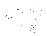
图1a.是包含半导体芯片和具有与引线指条分离的下置部分的引线框的一个模块的三维视图;Figure 1a. is a three-dimensional view of a module comprising a semiconductor chip and a lead frame with an underlying portion separated from the lead fingers;
图1b.是图1a的引线框的三维视图,示出了连接到引线框指条连接端的下置部分;FIG. 1b. is a three-dimensional view of the leadframe of FIG. 1a, showing the underlying portion connected to the leadframe finger bar connection;
图2是另一实施方案的三维视图,示出了包含半导体芯片和具有带下置部分的引线框的一个模块;2 is a three-dimensional view of another embodiment, showing a module comprising a semiconductor chip and a lead frame with an underlying portion;
图3是另一实施方案的三维视图,示出了包含半导体芯片和具有连接到引线指条的下置部分的引线框的一个模块;Figure 3 is a three-dimensional view of another embodiment, showing a module comprising a semiconductor chip and a leadframe having an underlying portion connected to a lead finger bar;
图4a是另一实施方案的三维视图,示出了包含半导体芯片、引线框、和模拟芯片的一个模块,此模拟芯片位于引线指条的下一层;Figure 4a is a three-dimensional view of another embodiment, showing a module comprising a semiconductor chip, a lead frame, and an analog chip positioned on the next layer of a lead finger bar;
图4b是两个实施方案的俯视图,左边的那个示出了包含由支架固定在图4a模拟芯片下一层的物体的模块,右边的那个示出了厚度相似于芯片并用条带固定到引线框连杆的物体;Figure 4b is a top view of two embodiments, the one on the left shows the module containing the object held by a standoff on a layer below the analog chip of Figure 4a, the one on the right shows a thickness similar to the chip and is secured to the leadframe with straps connecting rod objects;
图4c是图4b实施方案的剖面图;Figure 4c is a cross-sectional view of the embodiment of Figure 4b;
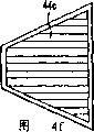
图4d-4f是具有各种形状的物体的俯视图;以及Figures 4d-4f are top views of objects having various shapes; and
图4g-4i是图4d-4f实施方案的相应剖面图。Figures 4g-4i are corresponding cross-sectional views of the embodiment of Figures 4d-4f.
本发明人认识到,通过平衡塑料封装件内的各个力,可以减少或避免弯曲。他们认识到,当引线框上面的塑料的厚度不同于引线框下面的厚度时,封装件就好象是双金属条,并根据温度而弯曲。为了减少或避免弯曲,本发明人在不同于引线框连接引线的层处的塑料中提供了额外的材料层,以便平衡各个力。在一个实施方案中,引线框材料的一部分被弯曲到不同于用作引线框其余部分的层,以便平衡各个力。在另一个实施方案中,引线指条被向下弯曲再回复向上,以便更好地平衡引线指条上的各个力。The inventors have realized that by balancing the various forces within the plastic package, bending can be reduced or avoided. They realized that when the thickness of the plastic above the leadframe was different than the thickness below the leadframe, the package behaved like a bimetallic strip and flexed in response to temperature. To reduce or avoid bending, the inventors provided an additional layer of material in the plastic at a different layer than the lead frame where the leads are connected, in order to balance the forces. In one embodiment, a portion of the leadframe material is bent to a different layer than the layer used for the remainder of the leadframe in order to balance the forces. In another embodiment, the lead fingers are bent down and back up to better balance the forces on the lead fingers.
如图1a所示,引线框22的下置连杆20在塑料包封剂26内的弯点24a和弯点24b处被弯曲到明显低于引线框22的引线指条32层面30的层28。层28被选择来提供双材料弯曲力,此力使模块36的引线指条32和集成电路芯片34上的某些或全部的力得到平衡。此外,下置连杆20从邻近封装件一端的位置延伸到邻近芯片34边沿的位置,以便使下置连杆20的面积最大,并使下置效应最大。于是,封装件的弯曲被减少或消除。下置连杆20最好具有A字形形状,以便在引线指条32所提供的空间内提供最大的面积,并提供机械强度和硬度。通过在下置连杆20内部提供几个支撑杆20’,也增加了稳定性。支撑杆20’被定向为平行于制模过程中液体塑料化合物的流向,使当液体塑料化合物填充物体时,连杆不被抬起。提供下置连杆20的尽可能最大面积,就提供了最大的力来抵消更高的引线指条32的力。下置连杆20最好与引线指条32平行,但在不同的平面上。弯点24a、24b通过使用工具夹住邻近连杆20的引线框22,然后用弯曲操作完成时以及下置连杆20被置于所希望的高度并平行于引线指条32时提供足够弯曲的工具,压住连杆20而实现。下置连杆20被设计成使到邻近引线指条32的最小间隔为32mil而到标称尺寸和放置的芯片34边沿的最小间隔为23mil,以便避免模块36中的电短路或机械接合。这些尺寸具有±1mil的公差。下置连杆20也能够被提供成在包封剂26内具有向下的斜坡。As shown in FIG. 1 a, the lower connecting
所希望的是,通过键合金属丝37连接到芯片34的键合焊点35的引线指条2位于包封剂26中高处。模块36和它所固定于其上的印制电路板(未示出)之间的应力被减少到引线指条32在模块36的包封剂26中被抬起的程度。因此,借助于把引线指条32提供成与其从包封剂26出来时那样高,就增强了到电路板的连接可靠性,同时,借助于提供下置连杆20来平衡包封剂26中的热应力,就减少了模块36内高放置所导致的应力。Desirably, the lead fingers 2 connected to the
在用塑料完成包封之后,引线指条32的连接端38(图1b)被切断,并把引线指条32弯曲到用以安装到印制电路板的位置。延伸出包封剂26的下置连杆20的连接端38’(图1b)被沿着包封剂26的边沿26’切断。现在,下置连杆20就与引线框22的其余部分和芯片34完全分离。After the encapsulation with plastic is complete, the connection ends 38 (FIG. 1b) of the
下置连杆20的引入将薄小外形塑料封装件(TSOP)的弯曲从3.5mil减少到了2mil,即减小了42%。这种40mil厚的塑料封装件使用了TCE约为13的模制包封剂,具有TCE为3.5的硅芯片以及由TCE约为4的合金42制造的引线框。引线指条32约为5mil厚,并位于距包封剂26顶部表面约9mil和距包封剂底部约26mil的地方。芯片34约为12mil厚,并且位于距包封剂26顶部表面约17mil处。引线指条32用厚约3mil的带条46a安装在芯片34上(图4)。下置连杆20被下置在比包封剂26内的引线指条32低约15mil处,以便提供弯曲改善。借助于增加下置连杆20的面积或增加下置量,能够获得弯曲的进一步改善。下置连杆20被设计成使到邻近引线指条32的最小间隔为32mil,而到芯片34端的最小间隔为23mil,以便避免模块36内的电短路或机械接合。The introduction of the
如图2所示,在变通实施方案中,引线指条32a的各个部分沿着区域32a’向下设置。在这种情况下,引线指条32a拥有弯点40a和40b,以便在比引线框22a的引线指条32a的层30更低的层28处提供下置区域32a’。除了或不用下置连杆20,能够提供引线指条32a的下置部分32a’。此外,具有下置区域33’的额外的指条33可以被提供在各引线指条32a之间的通常未被占用的空间内。As shown in FIG. 2, in an alternate embodiment, portions of
如图3所示,在另一个变通实施方案中,下置连杆20a能够被连接到一个或更多个引线指条32b。在这种情况下,弯点24a’和24b’在比引线框22a的引线指条32a的层30更低的层28处提供下置连杆20a。下置连杆20a连接于其上的引线指条32b,最好被电连接到地。如图3所示,如果希望的话,下置连杆20a可以被劈开。As shown in FIG. 3, in another alternative embodiment, the
如图4a所示,在另一个变通实施方案中,诸如模拟半导体芯片的物体44被提供在比引线指条32a的层30更低的包封剂26中的层28处。物体44提供力来平衡引线指条32a所提供的力。物体44可以被放置在与集成电路芯片34大致相同的层上。在这种情况下,物体44和芯片34都被安装在用来在装配过程中固定物体44和芯片34位置的带条46a和46b上。作为变通,如图4b和图4c所示,物体44’可以被放置在比芯片34低的位置。在这种情况下,支柱50用带条把物体44连接到引线指条32a。利用支柱的高度可以控制力。支柱50能够与物体44’成一整体,并且能够在浇注或冲压操作中制造。除了半导体之外,物体44、44’能用诸如合金42、殷钢、柯伐铁镍钴合金、或铜-殷钢-铜之类的金属来制造。也能够用诸如陶瓷或液晶聚合物之类的绝缘体来制造。如图4d-4f所示,物体44、44’可以有各种各样的形状44a、44b、44c。可以设计这些形状来控制装配过程中包封剂的流动,以便分裂大的平坦表面,从而将物体44、44’锁定在包封剂内的位置上。提供局部延伸通过物体44、44’的空洞,使平坦表面破裂,从而增强了与包封剂的接触,并避免了潮气引起的问题。As shown in Figure 4a, in another alternative embodiment, an
虽然此处详细描述了并在附图中阐述了本发明的几种实施方案及其修正,但显然,能够在设计下置元件的过程中作出多种进一步修正而不偏离本发明的范围。在上述说明书中,没有比所附权利要求更窄地限制本发明。给出的例子只是为了阐述而不是排他性的。While several embodiments of the invention and modifications thereto have been described in detail and illustrated in the drawings, it will be apparent that various further modifications can be made in the design of the underlying components without departing from the scope of the invention. In the foregoing specification, the invention is not limited more narrowly than by the appended claims. The examples given are for illustration only and are not exclusive.
Claims (38)
Applications Claiming Priority (3)
| Application Number | Priority Date | Filing Date | Title |
|---|---|---|---|
| US09/605,173 US6603195B1 (en) | 2000-06-28 | 2000-06-28 | Planarized plastic package modules for integrated circuits |
| US09/605,173 | 2000-06-28 | ||
| US09/605173 | 2000-06-28 |
Publications (2)
| Publication Number | Publication Date |
|---|---|
| CN1334603A true CN1334603A (en) | 2002-02-06 |
| CN1180478C CN1180478C (en) | 2004-12-15 |
Family
ID=24422553
Family Applications (1)
| Application Number | Title | Priority Date | Filing Date |
|---|---|---|---|
| CNB011226374A Expired - Fee Related CN1180478C (en) | 2000-06-28 | 2001-06-27 | Planarized Plastic Packaging Modules for Integrated Circuits |
Country Status (9)
| Country | Link |
|---|---|
| US (1) | US6603195B1 (en) |
| JP (1) | JP2002043494A (en) |
| KR (1) | KR100444242B1 (en) |
| CN (1) | CN1180478C (en) |
| BR (1) | BR0102606A (en) |
| CA (1) | CA2350057A1 (en) |
| HK (1) | HK1042591B (en) |
| MY (1) | MY119889A (en) |
| TW (1) | TWI231026B (en) |
Cited By (5)
| Publication number | Priority date | Publication date | Assignee | Title |
|---|---|---|---|---|
| CN101540307B (en) * | 2008-03-20 | 2010-10-20 | 力成科技股份有限公司 | Semiconductor packaging structure with pins on chip |
| CN101483166B (en) * | 2008-01-10 | 2011-09-07 | 力成科技股份有限公司 | Lead frame and semiconductor package structure with sunken spoiler connection structure |
| CN103624909A (en) * | 2012-08-24 | 2014-03-12 | 无锡华润安盛科技有限公司 | Clamp and method for reducing bending of plastic-sealed body |
| CN104956782A (en) * | 2013-01-09 | 2015-09-30 | 德克萨斯仪器股份有限公司 | Integrated circuit module |
| CN115274571A (en) * | 2022-09-30 | 2022-11-01 | 东屹半导体科技(江苏)有限公司 | Semiconductor packaging module with tilting component |
Families Citing this family (7)
| Publication number | Priority date | Publication date | Assignee | Title |
|---|---|---|---|---|
| US7323765B2 (en) * | 2004-10-13 | 2008-01-29 | Atmel Corporation | Die attach paddle for mounting integrated circuit die |
| JP4755214B2 (en) * | 2008-02-22 | 2011-08-24 | 力成科技股▲分▼有限公司 | Lead frame and semiconductor device using the same |
| US7812430B2 (en) * | 2008-03-04 | 2010-10-12 | Powertech Technology Inc. | Leadframe and semiconductor package having downset baffle paddles |
| US7750444B2 (en) * | 2008-05-19 | 2010-07-06 | Powertech Technology Inc. | Lead-on-chip semiconductor package and leadframe for the package |
| US9496214B2 (en) | 2013-05-22 | 2016-11-15 | Toyota Motor Engineering & Manufacturing North American, Inc. | Power electronics devices having thermal stress reduction elements |
| US20140374892A1 (en) * | 2013-06-24 | 2014-12-25 | Yit Meng LEE | Lead frame and semiconductor device using same |
| US9917039B2 (en) * | 2016-04-20 | 2018-03-13 | Amkor Technology, Inc. | Method of forming a semiconductor package with conductive interconnect frame and structure |
Family Cites Families (16)
| Publication number | Priority date | Publication date | Assignee | Title |
|---|---|---|---|---|
| US5229329A (en) * | 1991-02-28 | 1993-07-20 | Texas Instruments, Incorporated | Method of manufacturing insulated lead frame for integrated circuits |
| US5585600A (en) * | 1993-09-02 | 1996-12-17 | International Business Machines Corporation | Encapsulated semiconductor chip module and method of forming the same |
| US5686698A (en) | 1994-06-30 | 1997-11-11 | Motorola, Inc. | Package for electrical components having a molded structure with a port extending into the molded structure |
| US5789806A (en) | 1995-08-02 | 1998-08-04 | National Semiconductor Corporation | Leadframe including bendable support arms for downsetting a die attach pad |
| KR0184076B1 (en) * | 1995-11-28 | 1999-03-20 | 김광호 | Three-dimensional stacked package |
| JP3108856B2 (en) | 1995-12-28 | 2000-11-13 | ローム株式会社 | Resin package type semiconductor device and electronic circuit board mounting the same |
| JPH09186286A (en) * | 1996-01-05 | 1997-07-15 | Matsushita Electron Corp | Lead frame and semiconductor chip mounting method |
| US5872398A (en) * | 1996-01-11 | 1999-02-16 | Micron Technology, Inc. | Reduced stress LOC assembly including cantilevered leads |
| US6277225B1 (en) * | 1996-03-13 | 2001-08-21 | Micron Technology, Inc. | Stress reduction feature for LOC lead frame |
| KR100196285B1 (en) * | 1996-04-18 | 1999-06-15 | 윤종용 | Addition method of lead and chip, of lead on chip package |
| KR0174983B1 (en) * | 1996-05-10 | 1999-02-01 | 김광호 | Semiconductor chip mounting method using fluid adhesive and lead frame of LOC type semiconductor chip package |
| US5733800A (en) * | 1996-05-21 | 1998-03-31 | Micron Technology, Inc. | Underfill coating for LOC package |
| JPH09312367A (en) | 1996-05-23 | 1997-12-02 | Mitsubishi Electric Corp | High frequency semiconductor device |
| JPH1070230A (en) * | 1996-08-27 | 1998-03-10 | Hitachi Cable Ltd | LOC lead frame |
| KR100216991B1 (en) * | 1996-09-11 | 1999-09-01 | 윤종용 | Leadframe having adhesive layer |
| US6522299B2 (en) * | 1999-04-08 | 2003-02-18 | Cypress Semiconductor Corp. | PC card retractable antenna |
-
2000
- 2000-06-28 US US09/605,173 patent/US6603195B1/en not_active Expired - Lifetime
-
2001
- 2001-06-04 KR KR10-2001-0031081A patent/KR100444242B1/en not_active Expired - Fee Related
- 2001-06-07 CA CA002350057A patent/CA2350057A1/en not_active Abandoned
- 2001-06-21 MY MYPI20012927A patent/MY119889A/en unknown
- 2001-06-22 TW TW090115294A patent/TWI231026B/en not_active IP Right Cessation
- 2001-06-27 CN CNB011226374A patent/CN1180478C/en not_active Expired - Fee Related
- 2001-06-27 JP JP2001194587A patent/JP2002043494A/en active Pending
- 2001-06-28 BR BR0102606-2A patent/BR0102606A/en not_active IP Right Cessation
-
2002
- 2002-06-03 HK HK02104209.7A patent/HK1042591B/en not_active IP Right Cessation
Cited By (8)
| Publication number | Priority date | Publication date | Assignee | Title |
|---|---|---|---|---|
| CN101483166B (en) * | 2008-01-10 | 2011-09-07 | 力成科技股份有限公司 | Lead frame and semiconductor package structure with sunken spoiler connection structure |
| CN101540307B (en) * | 2008-03-20 | 2010-10-20 | 力成科技股份有限公司 | Semiconductor packaging structure with pins on chip |
| CN103624909A (en) * | 2012-08-24 | 2014-03-12 | 无锡华润安盛科技有限公司 | Clamp and method for reducing bending of plastic-sealed body |
| CN103624909B (en) * | 2012-08-24 | 2016-09-07 | 无锡华润安盛科技有限公司 | For reducing fixture and the method thereof of plastic-sealed body bending |
| CN104956782A (en) * | 2013-01-09 | 2015-09-30 | 德克萨斯仪器股份有限公司 | Integrated circuit module |
| CN104956782B (en) * | 2013-01-09 | 2018-05-11 | 德克萨斯仪器股份有限公司 | IC module |
| CN115274571A (en) * | 2022-09-30 | 2022-11-01 | 东屹半导体科技(江苏)有限公司 | Semiconductor packaging module with tilting component |
| CN115274571B (en) * | 2022-09-30 | 2022-12-16 | 东屹半导体科技(江苏)有限公司 | Semiconductor packaging module with tilting component |
Also Published As
| Publication number | Publication date |
|---|---|
| KR100444242B1 (en) | 2004-08-11 |
| HK1042591B (en) | 2005-05-13 |
| BR0102606A (en) | 2002-02-13 |
| HK1042591A1 (en) | 2002-08-16 |
| TWI231026B (en) | 2005-04-11 |
| MY119889A (en) | 2005-07-29 |
| KR20020001521A (en) | 2002-01-09 |
| JP2002043494A (en) | 2002-02-08 |
| US6603195B1 (en) | 2003-08-05 |
| CN1180478C (en) | 2004-12-15 |
| CA2350057A1 (en) | 2001-12-28 |
Similar Documents
| Publication | Publication Date | Title |
|---|---|---|
| CN1065662C (en) | Improved integrated chip package with reduced dimensions | |
| US5053852A (en) | Molded hybrid IC package and lead frame therefore | |
| US10796983B2 (en) | Positional relationship among components of semiconductor device | |
| CN1180478C (en) | Planarized Plastic Packaging Modules for Integrated Circuits | |
| KR19980032479A (en) | Surface installation TO-220 package and its manufacturing process | |
| CN1099131C (en) | Ball grid array semiconductor package | |
| US8030766B2 (en) | Semiconductor device | |
| US20130200507A1 (en) | Two-sided die in a four-sided leadframe based package | |
| JPH04269856A (en) | Lead frame; semiconductor integrated circuit device using it | |
| JP2000223639A (en) | Lead frame structure to prevent warpage of semiconductor package body | |
| JPH07161876A (en) | SEMICONDUCTOR INTEGRATED CIRCUIT DEVICE, METHOD FOR MANUFACTURING THE SAME, AND MOLD DIES USED FOR MANUFACTURING THE SAME | |
| WO2006091940A1 (en) | Integrated circuit package with lead stops | |
| JP3075617B2 (en) | Semiconductor integrated circuit device | |
| US8349655B2 (en) | Method of fabricating a two-sided die in a four-sided leadframe based package | |
| US6921967B2 (en) | Reinforced die pad support structure | |
| JPS6215844A (en) | Semiconductor lead frame | |
| US20050194698A1 (en) | Integrated circuit package with keep-out zone overlapping undercut zone | |
| JP2001024132A (en) | Deformation absorption type lead frame for semiconductor device | |
| KR950006434B1 (en) | Lead frame | |
| JP3061715B2 (en) | Resin-sealed semiconductor device | |
| KR100419950B1 (en) | manufacturing method of ball grid array semiconductor package using a flexible circuit board | |
| KR0177006B1 (en) | Semiconductor devices with composite lead configurations | |
| KR20120043867A (en) | Semiconductor package and method of manufacturing the same | |
| KR19990050846A (en) | Leadframe structure | |
| KR20010000425U (en) | semiconductor package |
Legal Events
| Date | Code | Title | Description |
|---|---|---|---|
| C10 | Entry into substantive examination | ||
| SE01 | Entry into force of request for substantive examination | ||
| C06 | Publication | ||
| PB01 | Publication | ||
| C14 | Grant of patent or utility model | ||
| GR01 | Patent grant | ||
| C17 | Cessation of patent right | ||
| CF01 | Termination of patent right due to non-payment of annual fee |
Granted publication date: 20041215 Termination date: 20120627 |