CN1402254A - Thin film magnetic storage device with storage unit contg. magnetic tunnel node - Google Patents
Thin film magnetic storage device with storage unit contg. magnetic tunnel node Download PDFInfo
- Publication number
- CN1402254A CN1402254A CN02128216A CN02128216A CN1402254A CN 1402254 A CN1402254 A CN 1402254A CN 02128216 A CN02128216 A CN 02128216A CN 02128216 A CN02128216 A CN 02128216A CN 1402254 A CN1402254 A CN 1402254A
- Authority
- CN
- China
- Prior art keywords
- data
- mentioned
- memory cell
- write
- current
- Prior art date
- Legal status (The legal status is an assumption and is not a legal conclusion. Google has not performed a legal analysis and makes no representation as to the accuracy of the status listed.)
- Granted
Links
Images







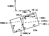


Classifications
-
- G—PHYSICS
- G11—INFORMATION STORAGE
- G11C—STATIC STORES
- G11C11/00—Digital stores characterised by the use of particular electric or magnetic storage elements; Storage elements therefor
- G11C11/02—Digital stores characterised by the use of particular electric or magnetic storage elements; Storage elements therefor using magnetic elements
- G11C11/14—Digital stores characterised by the use of particular electric or magnetic storage elements; Storage elements therefor using magnetic elements using thin-film elements
- G11C11/15—Digital stores characterised by the use of particular electric or magnetic storage elements; Storage elements therefor using magnetic elements using thin-film elements using multiple magnetic layers
-
- G—PHYSICS
- G11—INFORMATION STORAGE
- G11C—STATIC STORES
- G11C7/00—Arrangements for writing information into, or reading information out from, a digital store
- G11C7/18—Bit line organisation; Bit line lay-out
-
- G—PHYSICS
- G11—INFORMATION STORAGE
- G11C—STATIC STORES
- G11C11/00—Digital stores characterised by the use of particular electric or magnetic storage elements; Storage elements therefor
- G11C11/02—Digital stores characterised by the use of particular electric or magnetic storage elements; Storage elements therefor using magnetic elements
- G11C11/16—Digital stores characterised by the use of particular electric or magnetic storage elements; Storage elements therefor using magnetic elements using elements in which the storage effect is based on magnetic spin effect
-
- G—PHYSICS
- G11—INFORMATION STORAGE
- G11C—STATIC STORES
- G11C11/00—Digital stores characterised by the use of particular electric or magnetic storage elements; Storage elements therefor
- G11C11/02—Digital stores characterised by the use of particular electric or magnetic storage elements; Storage elements therefor using magnetic elements
- G11C11/16—Digital stores characterised by the use of particular electric or magnetic storage elements; Storage elements therefor using magnetic elements using elements in which the storage effect is based on magnetic spin effect
- G11C11/161—Digital stores characterised by the use of particular electric or magnetic storage elements; Storage elements therefor using magnetic elements using elements in which the storage effect is based on magnetic spin effect details concerning the memory cell structure, e.g. the layers of the ferromagnetic memory cell
-
- G—PHYSICS
- G11—INFORMATION STORAGE
- G11C—STATIC STORES
- G11C11/00—Digital stores characterised by the use of particular electric or magnetic storage elements; Storage elements therefor
- G11C11/02—Digital stores characterised by the use of particular electric or magnetic storage elements; Storage elements therefor using magnetic elements
- G11C11/16—Digital stores characterised by the use of particular electric or magnetic storage elements; Storage elements therefor using magnetic elements using elements in which the storage effect is based on magnetic spin effect
- G11C11/165—Auxiliary circuits
- G11C11/1653—Address circuits or decoders
- G11C11/1655—Bit-line or column circuits
-
- G—PHYSICS
- G11—INFORMATION STORAGE
- G11C—STATIC STORES
- G11C11/00—Digital stores characterised by the use of particular electric or magnetic storage elements; Storage elements therefor
- G11C11/02—Digital stores characterised by the use of particular electric or magnetic storage elements; Storage elements therefor using magnetic elements
- G11C11/16—Digital stores characterised by the use of particular electric or magnetic storage elements; Storage elements therefor using magnetic elements using elements in which the storage effect is based on magnetic spin effect
- G11C11/165—Auxiliary circuits
- G11C11/1653—Address circuits or decoders
- G11C11/1657—Word-line or row circuits
-
- G—PHYSICS
- G11—INFORMATION STORAGE
- G11C—STATIC STORES
- G11C11/00—Digital stores characterised by the use of particular electric or magnetic storage elements; Storage elements therefor
- G11C11/02—Digital stores characterised by the use of particular electric or magnetic storage elements; Storage elements therefor using magnetic elements
- G11C11/16—Digital stores characterised by the use of particular electric or magnetic storage elements; Storage elements therefor using magnetic elements using elements in which the storage effect is based on magnetic spin effect
- G11C11/165—Auxiliary circuits
- G11C11/1675—Writing or programming circuits or methods
-
- G—PHYSICS
- G11—INFORMATION STORAGE
- G11C—STATIC STORES
- G11C8/00—Arrangements for selecting an address in a digital store
- G11C8/12—Group selection circuits, e.g. for memory block selection, chip selection, array selection
Landscapes
- Engineering & Computer Science (AREA)
- Computer Hardware Design (AREA)
- Mram Or Spin Memory Techniques (AREA)
- Hall/Mr Elements (AREA)
- Semiconductor Memories (AREA)
Abstract
在隧道磁电阻元件(100a)中,第一和第二自由磁化层(103)具有对应存储数据的磁化方向。第一和第二自由磁化层夹住非磁性导电体形成的中间层(107)来配置。数据写入时,中间层(107)中流过对应写入的存储数据的电平的方向的数据写入电流。通过由流过中间层的电流产生的磁场将第一和第二自由磁化层磁化为环状。
In the tunnel magnetoresistance element (100a), the first and second free magnetization layers (103) have magnetization directions corresponding to stored data. The first and second free magnetization layers are arranged to sandwich an intermediate layer (107) formed of a non-magnetic conductor. When writing data, a data writing current in a direction corresponding to the level of stored data to be written flows through the intermediate layer (107). The first and second free magnetization layers are magnetized in a ring shape by a magnetic field generated by a current flowing through the intermediate layer.
Description
技术领域technical field
本发明涉及一种薄膜磁存储装置,尤其涉及备有含磁隧道结(MTJ:Magnetic Tunnel Junction)的存储器单元的随机存取存储器。The present invention relates to a thin film magnetic storage device, in particular to a random access memory equipped with a memory unit containing a Magnetic Tunnel Junction (MTJ: Magnetic Tunnel Junction).
背景技术Background technique
作为低功耗可存储非易失性数据的存储装置,MRAM(MagneticRandom memory)器件受到关注。MRAM器件是使用在半导体集成电路上形成的多个薄膜磁体进行非易失性数据的存储,可对各个薄膜磁体进行随机存取的存储装置。As a low-power storage device that can store non-volatile data, MRAM (Magnetic Random memory) devices have attracted attention. The MRAM device is a storage device that uses multiple thin-film magnets formed on a semiconductor integrated circuit to store non-volatile data, and can perform random access to each thin-film magnet.
尤其,近年来,发表了通过将利用磁隧道结的薄膜磁体用作存储器单元可飞速促进MRAM器件性能进步。对于备有含磁隧道结的存储器单元的MRAM器件,在2000年2月的ISSCC Digest of TechnicalPapers,TA7.2的“A 10ns Read and Write Non-Volatile Memory ArrayUsing a Magnetic Tunnel Junction and FET Switch in each Cell”和2000年2月的ISSCC Digest of Technical Papers,TA7.3的“NonvolatileRAM based on Magnetic Tunnel Junction Element”等技术文献中公开。In particular, in recent years, it has been reported that the performance of an MRAM device can be rapidly improved by using a thin-film magnet utilizing a magnetic tunnel junction as a memory cell. For MRAM devices with memory cells containing magnetic tunnel junctions, "A 10ns Read and Write Non-Volatile Memory Array Using a Magnetic Tunnel Junction and FET Switch in each Cell" in ISSCC Digest of Technical Papers, TA7.2 in February 2000 " and ISSCC Digest of Technical Papers in February 2000, TA7.3 "NonvolatileRAM based on Magnetic Tunnel Junction Element" and other technical documents.
图48是表示具有磁隧道结的存储器单元(下面简称MTJ存储器单元)的结构和数据读出动作的概念图。FIG. 48 is a conceptual diagram showing the structure and data read operation of a memory cell having a magnetic tunnel junction (hereinafter referred to as an MTJ memory cell).
参考图48,MTJ存储器单元具有对应存储数据的数据电平变化电阻值的隧道磁电阻元件TMR和数据读出时形成通过隧道磁电阻元件TMR的传感电流的路径的存取晶体管ATR。存取晶体管ATR例如用场效应晶体管形成,耦合于隧道磁电阻元件TMR和接地电压VSS之间。Referring to FIG. 48 , the MTJ memory cell has a tunneling magneto-resistance element TMR having a data level change resistance value corresponding to stored data, and an access transistor ATR forming a path for a sense current passing through the tunnel magneto-resistance element TMR during data reading. The access transistor ATR is formed by, for example, a field effect transistor, and is coupled between the tunnel magnetoresistive element TMR and the ground voltage VSS.
隧道磁电阻元件TMR包括具有一定方向的固定磁场的铁磁性层(下面简称为固定磁化层)FL和磁化为根据从外部施加的磁场变化的方向上的铁磁性层(下面简称自由磁化层)VL。在固定磁化层FL和自由磁化层VL之间配置绝缘膜形成的隧道势垒层TB。自由磁化层VL对应存储数据的电平磁化为与固定磁化层FL相同方向或与固定磁化层FL不同方向上。The tunnel magnetoresistive element TMR includes a ferromagnetic layer (hereinafter simply referred to as a fixed magnetization layer) FL having a fixed magnetic field in a certain direction and a ferromagnetic layer (hereinafter referred to as a free magnetization layer) VL magnetized in a direction that varies according to a magnetic field applied from the outside. . A tunnel barrier layer TB formed of an insulating film is arranged between the fixed magnetization layer FL and the free magnetization layer VL. The level magnetization of the free magnetization layer VL corresponding to the stored data is in the same direction as that of the fixed magnetization layer FL or in a direction different from that of the fixed magnetization layer FL.
对于MTJ存储器单元,配置指示数据写入的写入字线WWL和指示数据读出的读出字线RWL以及作为在数据读出时和数据写入时传送对应存储数据的电平的电信号的数据线的位线BL。For an MTJ memory cell, a write word line WWL indicating data writing and a read word line RWL indicating data reading are configured, as well as an electrical signal that transmits a level corresponding to stored data when data is read and when data is written. The data line is the bit line BL.
数据读出时,存取晶体管ATR对应读出字线RWL的激活被接通。由此,位线BL~隧道磁电阻元件TMR~存取晶体管ATR~接地电压VSS的电流路径中可流过传感电流Is。When reading data, the access transistor ATR is turned on corresponding to the activation of the read word line RWL. Accordingly, the sense current Is can flow in the current path from the bit line BL to the tunnel magnetoresistive element TMR to the access transistor ATR to the ground voltage VSS.
隧道磁电阻元件TMR的电阻值对应固定磁化层FL和自由磁化层VL的磁化方向的相对关系变化。具体说,固定磁化层FL的磁化方向和自由磁化层VL中写入的磁化方向对齐时,与二者的磁化方向不同(反平行:antiparallel)时相比,隧道磁电阻元件TMR的电阻值减小。下面本说明书中,分别与存储数据1和0对应的隧道磁电阻元件的电阻值分别用R1和R0表示。其中R1>R0。The resistance value of the tunnel magnetoresistance element TMR changes in accordance with the relative relationship between the magnetization directions of the fixed magnetization layer FL and the free magnetization layer VL. Specifically, when the magnetization direction of the fixed magnetization layer FL is aligned with the magnetization direction written in the free magnetization layer VL, the resistance value of the tunnel magnetoresistance element TMR decreases compared to when the magnetization directions of the two are different (antiparallel). Small. In the following specification, the resistance values of the tunnel magneto-resistance elements corresponding to the
这样,隧道磁电阻元件TMR对应磁化方向变化其电阻值。因此,分别对应隧道磁电阻元件TMR中的自由磁化层VL的2个磁化方向和存储数据的电平(1和0),可执行数据存储。即,自由磁化层VL相当于MTJ存储器单元的存储节点。In this way, the tunnel magnetoresistance element TMR changes its resistance value in accordance with the magnetization direction. Therefore, data storage can be performed corresponding to the two magnetization directions of the free magnetization layer VL in the tunnel magnetoresistance element TMR and the levels (1 and 0) of the storage data, respectively. That is, free magnetization layer VL corresponds to the storage node of the MTJ memory cell.
由于传感电流Is在隧道磁电阻元件TMR产生的电压变化对应自由磁化层VL的磁化方向,即存储数据电平而不同。由此,将位线BL预充电到一定电压的状态后,隧道磁电阻元件TMR中不流过传感电流Is,通过监视位线BL的电压电平变化可读出MTJ存储器单元的存储数据。The voltage change generated by the sensing current Is in the tunnel magnetoresistance element TMR is different corresponding to the magnetization direction of the free magnetization layer VL, that is, the stored data level. Thus, after the bit line BL is precharged to a certain voltage, the sensing current Is does not flow in the tunnel magnetoresistive element TMR, and the stored data of the MTJ memory cell can be read by monitoring the voltage level change of the bit line BL.
图49是说明对MTJ存储器单元的数据写入动作的概念图;FIG. 49 is a conceptual diagram illustrating an operation of writing data to an MTJ memory cell;
参考图49,在数据写入时,读出字线RWL不激活,存取晶体管ATR接通。该状态下,将自由磁化层VL磁化为对应写入数据的方向的数据写入电流分别流向写入字线WWL和位线BL。自由磁化层VL的磁化方向通过分别流过写入字线WWL和位线BL的数据写入电流的方向组合决定。Referring to FIG. 49, during data writing, read word line RWL is inactive, and access transistor ATR is turned on. In this state, a data writing current that magnetizes free magnetization layer VL in a direction corresponding to writing data flows to writing word line WWL and bit line BL, respectively. The magnetization direction of free magnetization layer VL is determined by a combination of directions of data write current flowing through write word line WWL and bit line BL, respectively.
图50是说明数据写入时数据写入电流的方向和磁化方向的关系的概念图。FIG. 50 is a conceptual diagram illustrating the relationship between the direction of the data writing current and the magnetization direction during data writing.
参考图50,横轴Hx表示由流过位线BL的数据写入电流产生的数据写入磁场H(BL)的方向。另一方面,纵轴Hy表示由流过写入字线WWL的数据写入电流产生的数据写入磁场H(WWL)的方向。Referring to FIG. 50, the horizontal axis Hx represents the direction of the data write magnetic field H(BL) generated by the data write current flowing through the bit line BL. On the other hand, the vertical axis Hy represents the direction of the data write magnetic field H(WWL) generated by the data write current flowing through the write word line WWL.
自由磁化层VL的磁化方向仅在数据写入磁场H(BL)和H(WWL)的和到达图中所示的磁滞特性线的外侧区域时可被重新改写。即,施加的数据写入磁场为与磁滞特性线的内侧区域相当的强度时,不改变自由磁化层VL的磁化方向。The magnetization direction of the free magnetization layer VL can be rewritten only when the sum of the data write magnetic fields H(BL) and H(WWL) reaches the outer region of the hysteresis characteristic line shown in the figure. That is, when the applied data writing magnetic field has a strength corresponding to the inner region of the hysteresis characteristic line, the magnetization direction of the free magnetization layer VL is not changed.
因此,为通过数据写入动作更新隧道磁电阻元件TMR的存储内容,需要在写入字线WWL和位线BL二者中流过规定电平以上的电流。隧道磁电阻元件TMR中暂时存储的磁化方向,即存储数据在执行新的数据写入之前非易失地保持。Therefore, in order to update the stored content of the tunnel magnetoresistive element TMR through the data write operation, it is necessary to flow a current of a predetermined level or higher through both the write word line WWL and the bit line BL. The magnetization direction temporarily stored in the tunnel magneto-resistance element TMR, that is, the stored data is non-volatilely held until new data writing is performed.
数据读出动作时,位线BL中流过传感电流Is。但是,传感电流Is一般设定得比上述数据写入电流小1~2个数量级,因此由于传感电流Is的影响在数据读出时MTJ存储器单元的存储数据被误改写的可能性小。During the data read operation, the sense current Is flows through the bit line BL. However, the sense current Is is generally set to be 1 to 2 orders of magnitude smaller than the above-mentioned data writing current, so the possibility of erroneous rewriting of stored data in the MTJ memory cell during data reading due to the influence of the sense current Is is small.
但是,使用这种隧道磁电阻元件TMR的MRAM器件中,随着存储器单元尺寸缩小,产生下面所述的问题。However, in an MRAM device using such a tunnel magneto-resistive element TMR, problems as described below arise as the memory cell size shrinks.
MTJ存储器单元中,通过自由磁化层VL的磁化方向存储存储数据,但为改写自由磁化层VL的磁化方向需要施加的磁场强度(下面叫做反转磁场强度)在磁性层厚度为T、磁性层的磁化方向的长度为L时与T/L成比例。因此,缩小磁场强度单元大小时,随着平面方向尺寸的缩小(scaling)反转磁场强度增大。In the MTJ memory cell, the stored data is stored through the magnetization direction of the free magnetization layer VL, but the magnetic field strength (hereinafter referred to as the reversal magnetic field strength) that needs to be applied to rewrite the magnetization direction of the free magnetization layer VL is when the thickness of the magnetic layer is T, the magnetic layer When the length of the magnetization direction is L, it is proportional to T/L. Therefore, when the size of the magnetic field strength unit is reduced, the reversal magnetic field strength increases as the dimension in the plane direction is reduced (scaling).
随着磁场强度单元尺寸的缩小,在MTJ存储器单元外部和内部固定磁化层和自由磁化层之间产生的磁场干扰增大。由此,数据写入需要的数据写入磁场的阈值(与图50中的磁滞特性线相当)依赖写入数据的图形而变化,依赖数据写入西磁场的方向而变为非对称形状。As the size of the magnetic field strength cell shrinks, the magnetic field interference generated between the fixed magnetization layer and the free magnetization layer outside and inside the MTJ memory cell increases. Thus, the threshold value of the data writing magnetic field required for data writing (corresponding to the hysteresis characteristic line in FIG. 50 ) changes depending on the pattern of the writing data, and becomes asymmetrical depending on the direction of the data writing magnetic field.
由于这种现象,MTJ存储器单元缩小变得困难,随着存储器单元尺寸缩小产生消耗电流增大等问题。Due to this phenomenon, it becomes difficult to reduce the size of the MTJ memory cell, and problems such as an increase in current consumption occur as the size of the memory cell decreases.
为解决这种问题,美国专利(USP)6,166,948中公开一种技术:将MTJ存储器单元的自由磁化层有具有不同的磁矩的2层的铁磁性层形成。下面将这种由2层磁性层形成自由磁化层的构造叫做2层存储节点构造。与此相反,将图48和图49所示的由单层磁性层形成自由磁化层的构造叫做单层存储节点构造。In order to solve this problem, US Patent (USP) 6,166,948 discloses a technique in which a free magnetization layer of an MTJ memory cell is formed of two ferromagnetic layers having different magnetic moments. Hereinafter, such a structure in which two magnetic layers form a free magnetization layer is called a two-layer storage node structure. In contrast, the structure in which a free magnetization layer is formed of a single magnetic layer shown in FIGS. 48 and 49 is called a single-layer storage node structure.
图51是表示具有2层存储节点构造的已有隧道磁电阻元件结构的截面图。Fig. 51 is a cross-sectional view showing the structure of a conventional tunnel magnetoresistive element having a two-layer storage node structure.
参考图51,已有的隧道磁电阻元件包含反铁磁层AFL、固定磁化层FL、自由磁化层VL1,VL2、固定磁化层FL和自由磁化层VL1之间形成的隧道势垒层TB、自由磁化层VL1,VL2之间形成的中间层IML。中间层IML用非磁性体形成。包含图51所示的隧道磁电阻元件的MTJ存储器单元中,对应固定磁化层FL和自由磁化层VL1的磁化方向的相对关系存储存储数据。Referring to FIG. 51, the existing tunnel magnetoresistive element includes an antiferromagnetic layer AFL, a fixed magnetization layer FL, free magnetization layers VL1, VL2, a tunnel barrier layer TB formed between the fixed magnetization layer FL and the free magnetization layer VL1, a free The intermediate layer IML is formed between the magnetization layers VL1, VL2. The intermediate layer IML is formed of a non-magnetic material. In the MTJ memory cell including the tunnel magnetoresistive element shown in FIG. 51, stored data is stored in correspondence with the relative relationship between the magnetization directions of the fixed magnetization layer FL and the free magnetization layer VL1.
自由磁化层VL1,VL2夹持中间层IM1L配置。自由磁化层VL1的磁矩比自由磁化层VL2大。因此,变化磁化方向的磁化阈值是自由磁化层VL1比自由磁化层VL2大。The free magnetization layers VL1, VL2 are configured to sandwich the intermediate layer IM1L. The magnetic moment of free magnetization layer VL1 is larger than that of free magnetization layer VL2. Therefore, the magnetization threshold for changing the magnetization direction is larger for the free magnetization layer VL1 than for the free magnetization layer VL2.
由于磁矩有强弱,因此自由磁化层VL1的磁化方向变化时,为与自由磁化层VL1之间形成磁化环路,自由磁化层VL2的磁化方向也随着变化。Since the magnetic moment is strong or weak, when the magnetization direction of the free magnetization layer VL1 changes, the magnetization direction of the free magnetization layer VL2 also changes accordingly to form a magnetization loop with the free magnetization layer VL1.
图52是说明图51所示隧道磁电阻元件的磁化的磁滞曲线图。图52中,示出数据写入磁场H引起的自由磁化层VL1,VL2的易磁化轴方向的磁化举动。FIG. 52 is a hysteresis curve diagram illustrating the magnetization of the tunnel magnetoresistive element shown in FIG. 51. FIG. FIG. 52 shows the magnetization behavior in the direction of the easy axis of magnetization of the free magnetization layers VL1 and VL2 caused by the data writing magnetic field H. In FIG.
参考图52,首先,说明数据写入磁场在负方向增大时的磁化方向的变化。Referring to FIG. 52, first, a change in the magnetization direction when the data writing magnetic field increases in the negative direction will be described.
首先,H>H01区域(状态1A)中,自由磁化层VL1,VL2都被磁化为正方向(右方向)。接着,变化为H<H01时(状态2A),仅磁矩小的自由磁化层VL2的磁化方向反转。First, in the H>H01 region (state 1A), both the free magnetization layers VL1 and VL2 are magnetized in the positive direction (right direction). Next, when the change becomes H<H01 (state 2A), only the magnetization direction of the free magnetization layer VL2 having a small magnetic moment is reversed.
另外,将磁场变化为负方向,进入超出阈值-H02的区域(状态3A)时,磁矩大的自由磁化层VL1的磁化方向从正方向(右侧)变化为负方向(左侧)。随之而来的是自由磁化层VL2的磁化方向也从状态2A反转。In addition, when the magnetic field is changed to a negative direction and enters a region exceeding the threshold -H02 (state 3A), the magnetization direction of the free magnetization layer VL1 with a large magnetic moment changes from a positive direction (right side) to a negative direction (left side). It follows that the magnetization direction of the free magnetization layer VL2 is also reversed from state 2A.
此外,数据写入磁场H在负方向增大时,进入H<-H03的区域(状态4A)时,自由磁化层VL1,VL2二者中,磁化方向变化为负方向(左侧)。In addition, when the data write magnetic field H increases in the negative direction and enters the region of H<-H03 (state 4A), the magnetization directions of both free magnetization layers VL1 and VL2 change to the negative direction (left side).
接着说明数据写入磁场H在正方向增大时的磁化方向的变化。Next, the change in the magnetization direction when the data writing magnetic field H increases in the positive direction will be described.
H<-H01区域(状态4B)中,自由磁化层VL1,VL2都被磁化为负方向(左方向)。接着,变化为H>-H01时(状态3B),仅磁矩小的自由磁化层VL2的磁化方向反转。In the H<-H01 region (state 4B), both the free magnetization layers VL1 and VL2 are magnetized in the negative direction (left direction). Next, when the change is H>-H01 (state 3B), only the magnetization direction of the free magnetization layer VL2 having a small magnetic moment is reversed.
另外,将磁场变化为正方向,进入超出阈值H02的区域(状态2B)时,磁矩大的自由磁化层VL1的磁化方向从负方向(左侧)变化为正方向(右侧)。随之而来的是自由磁化层VL2的磁化方向也从状态3B反转。In addition, when the magnetic field is changed to a positive direction and enters a region exceeding the threshold H02 (state 2B), the magnetization direction of the free magnetization layer VL1 with a large magnetic moment changes from the negative direction (left side) to the positive direction (right side). It follows that the magnetization direction of the free magnetization layer VL2 is also reversed from state 3B.
此外,数据写入磁场H在正方向增大时,进入H>H03的区域(状态1B)时,自由磁化层VL1,VL2二者中,磁化方向变化为正方向(右侧)。In addition, when the data write magnetic field H increases in the positive direction and enters the region of H>H03 (state 1B), the magnetization directions of the free magnetization layers VL1 and VL2 change to the positive direction (right side).
这样,用分别具有不同的磁化阈值(磁矩)的铁磁层形成并在其间夹持作为非磁性层的中间层来构成自由磁化层,通过将自由磁化层的磁场在上/下层彼此反转的状态用作数据存储状态,可减轻自由磁化层的反转磁场强度。数据存储状态中,2层的自由磁化层被磁化为环状,因此MTJ存储器单元中磁力线不扩张,磁场干扰产生的坏影响也可被抑制。In this way, the free magnetization layer is formed by forming ferromagnetic layers each having a different magnetization threshold value (magnetic moment) and sandwiching an intermediate layer as a nonmagnetic layer in between, by reversing the magnetic field of the free magnetization layer to each other in the upper/lower layer The state of is used as a data storage state, which can relieve the reversal magnetic field strength of the free magnetization layer. In the data storage state, the two free magnetization layers are magnetized in a ring shape, so the magnetic force lines in the MTJ memory cell do not expand, and the adverse effects of magnetic field interference can also be suppressed.
但是,如图51所示的2层存储节点构造的MTJ存储器单元中,自由磁化层VL1,VL2必须具有彼此不同的磁化阈值(磁矩),因此需要层叠材质和厚度等不同的2个磁性层,制造装置和制造工序复杂化。However, in an MTJ memory cell with a two-layer storage node structure as shown in FIG. 51, the free magnetization layers VL1 and VL2 must have different magnetization thresholds (magnetic moments) from each other, so it is necessary to laminate two magnetic layers of different materials and thicknesses. , The manufacturing device and manufacturing process are complicated.
尤其,如图52所示,自由磁化层VL1,VL2之间的磁矩的差对数据存储状态产生的影响大,因此由于在制造时的磁矩偏差,恐怕会使MTJ存储器单元的数据存储特性产生大变化。In particular, as shown in FIG. 52, the difference in the magnetic moment between the free magnetization layers VL1 and VL2 has a great influence on the data storage state, so the data storage characteristics of the MTJ memory cell may be affected due to the deviation of the magnetic moment during manufacture. Make big changes.
如图48,图49和图52所示,MTJ存储器单元中,磁化为对应存储数据的方向的自由磁化层VL,VL1,VL2与具有固定磁化方向的固定磁化层FL以及反铁磁层AFL接近配置,因此自由磁化层的磁化特性对应存储数据电平变得不均匀。As shown in Figure 48, Figure 49 and Figure 52, in the MTJ memory cell, the free magnetization layers VL, VL1, VL2, which are magnetized in the direction corresponding to the stored data, are close to the fixed magnetization layer FL and the antiferromagnetic layer AFL with a fixed magnetization direction. configuration, so that the magnetization characteristics of the free magnetization layer become non-uniform corresponding to the stored data level.
图53是说明单层存储节点构造的MTJ存储器单元的磁化特性的不均匀性的概念图。FIG. 53 is a conceptual diagram illustrating non-uniformity in magnetization characteristics of an MTJ memory cell having a single-layer storage node structure.
参考图53,固定磁化层FL和反铁磁层AFL具有相同的固定的磁化方向。反铁磁层AFL配置来更牢固地固定固定磁化层FL的磁化方向。Referring to FIG. 53, the fixed magnetization layer FL and the antiferromagnetic layer AFL have the same fixed magnetization direction. The antiferromagnetic layer AFL is configured to more firmly fix the magnetization direction of the fixed magnetization layer FL.
用作存储节点的自由磁化层VL对应存储数据的电平磁化到正方向(+方向)和负方向(-方向)之一。图53中,与固定磁化层FL相同方向的磁化方向定义为正方向,与固定磁化层FL反平行方向的磁化方向定义为负方向。The free magnetization layer VL serving as a storage node is magnetized to one of a positive direction (+ direction) and a negative direction (−direction) corresponding to a level of stored data. In FIG. 53 , the magnetization direction in the same direction as the fixed magnetization layer FL is defined as a positive direction, and the magnetization direction in an antiparallel direction to the fixed magnetization layer FL is defined as a negative direction.
这样,由于多个磁性层接近设置,来自反铁磁层AFL和固定磁化层FL的磁场静磁耦合,自由磁化层VL中,在易磁化轴方向上施加相同的磁场ΔHp。相同的磁场ΔHp作用在与固定磁化层FL反平行方向,即负方向上。由于这种相同磁场ΔHp的存在,自由磁化层VL的磁化特性依赖磁场方向为非对称的。In this way, since the magnetic layers are arranged close to each other, the magnetic fields from the antiferromagnetic layer AFL and the fixed magnetization layer FL are magnetostatically coupled, and in the free magnetization layer VL, the same magnetic field ΔHp is applied in the direction of the easy axis of magnetization. The same magnetic field ΔHp acts in a direction antiparallel to the fixed magnetization layer FL, ie, in a negative direction. Due to the existence of this same magnetic field ΔHp, the magnetization characteristic of the free magnetization layer VL is asymmetrical depending on the direction of the magnetic field.
图54是说明图53所示的自由磁化层VL的磁化特性的磁滞曲线图。图54中,表示易磁化轴方向的数据写入磁场Hex引起的自由磁化层VL的磁化举动。FIG. 54 is a hysteresis graph illustrating the magnetization characteristics of the free magnetization layer VL shown in FIG. 53 . FIG. 54 shows the magnetization behavior of the free magnetization layer VL caused by the data writing magnetic field Hex in the direction of the easy axis of magnetization.
参考图54,为将磁化为负方向的自由磁化层VL磁化到正方向,需要施加超出+Hsp的正方向的磁场Hex。相反,为将磁化为正方向的自由磁化层VL磁化到负方向,需要施加超出-Hsn的负方向的磁场Hex。Referring to FIG. 54 , in order to magnetize the free magnetization layer VL magnetized in the negative direction to the positive direction, it is necessary to apply a magnetic field Hex in the positive direction exceeding +Hsp. Conversely, in order to magnetize the free magnetization layer VL magnetized in the positive direction to the negative direction, it is necessary to apply a magnetic field Hex in the negative direction exceeding -Hsn.
这里,由于与固定磁化层FL之间的静磁耦合产生的相同磁场ΔHp的影响,磁化到正方向的阈值Hsp比磁化到负方向的阈值Hsn仅大ΔHp。这样,对应施加磁场方向,自由磁化层VL的磁化特性不对称,因此依赖于对MTJ存储器单元的写入数据的电平,需要向自由磁化层VL施加的磁场强度不同。为将这种隧道磁电阻元件用作存储器单元,写入某一数据电平时,都需要施加超出大的磁化阈值的磁场。即,在将自由磁化层VL磁化为负方向时需要施加用于产生超出磁化阈值Hsp的磁场的数据写入电流。从而,这种情况下,数据写入电流变得不必要地大。由此,产生功耗增大,布线电流密度增加引起的布线可靠性降低这类问题。Here, the threshold Hsp of magnetization to the positive direction is greater than the threshold Hsn of magnetization to the negative direction by only ΔHp due to the influence of the same magnetic field ΔHp generated by the magnetostatic coupling with the fixed magnetization layer FL. As described above, since the magnetization characteristics of free magnetization layer VL are asymmetrical in accordance with the direction of the applied magnetic field, the strength of the magnetic field to be applied to free magnetization layer VL needs to be different depending on the level of data written to the MTJ memory cell. In order to use such a tunnel magnetoresistive element as a memory cell, it is necessary to apply a magnetic field exceeding a large magnetization threshold whenever a certain data level is written. That is, when magnetizing free magnetization layer VL in the negative direction, it is necessary to apply a data write current for generating a magnetic field exceeding magnetization threshold value Hsp. Therefore, in this case, the data writing current becomes unnecessarily large. As a result, power consumption increases and wiring reliability decreases due to an increase in wiring current density.
这种现象在2层存储节点构造的隧道磁电阻元件中同样存在。This phenomenon also exists in tunnel magnetoresistive elements with a two-layer storage node structure.
图55是说明2层存储节点构造的MTJ存储器单元的磁化特性的不均匀性的概念图。FIG. 55 is a conceptual diagram illustrating non-uniformity in magnetization characteristics of an MTJ memory cell having a two-layer storage node structure.
参考图55,即便是2层存储节点构造的隧道磁电阻元件,与单层存储节点构造同样,在自由磁化层VL1中,由于反铁磁层AFL和固定磁化层FL之间的静磁耦合,在易磁化轴方向上施加相同磁场ΔHp。由此,自由磁化层VL1,VL2的易磁化轴方向的磁化举动不对称。Referring to FIG. 55 , even for a tunnel magneto-resistive element with a two-layer storage node structure, as in the single-layer storage node structure, in the free magnetization layer VL1, due to the magnetostatic coupling between the antiferromagnetic layer AFL and the fixed magnetization layer FL, Apply the same magnetic field ΔHp in the direction of the easy axis of magnetization. Accordingly, the magnetization behavior in the direction of the easy magnetization axis of the free magnetization layers VL1 and VL2 is asymmetric.
图56是说明图55所示的自由磁化层VL的磁化特性的磁滞曲线图。FIG. 56 is a hysteresis curve diagram illustrating the magnetization characteristics of the free magnetization layer VL shown in FIG. 55 .
参考图56,由于与固定磁化层FL之间的静磁耦合产生的相同磁场ΔHp的影响,易磁化轴方向的数据写入磁场Hex引起的自由磁化层VL1,VL2的磁化举动与图52所示的逻辑特性相比,是仅有ΔHp的偏移的特性。即,相对针对图52所示的正方向的施加磁场的阈值+H01,+H02,+H03,针对负方向的磁场的阈值-H01’,-H02’,-H03’仅分别错开ΔHp,相对正方向的磁场和负方向的磁场磁化特性不对称。即,H01-|-H01’|=H02-|-H02’|=H03-|-H03’|=ΔHp。Referring to Figure 56, due to the influence of the same magnetic field ΔHp generated by the magnetostatic coupling with the fixed magnetization layer FL, the magnetization behavior of the free magnetization layers VL1 and VL2 caused by the data writing magnetic field Hex in the direction of the easy axis of magnetization is the same as that shown in Figure 52 Compared with the logic characteristic of , it is a characteristic with only a shift of ΔHp. That is, relative to the thresholds +H01, +H02, +H03 of the applied magnetic field in the positive direction shown in FIG. The magnetization characteristics of the magnetic field in the negative direction and the magnetic field in the negative direction are asymmetric. That is, H01-|-H01'|=H02-|-H02'|=H03-|-H03'|=ΔHp.
这样,在单层存储节点构造和2层存储节点构造的任一个的隧道磁电阻元件中引起磁场特性的不对称,需要数据写入电流的电平不必要地增大。As described above, asymmetry in the magnetic field characteristic is caused in the tunnel magnetoresistive element of either the single-layer storage node structure or the two-layer storage node structure, and the level of the data writing current needs to be increased unnecessarily.
发明内容Contents of the invention
本发明的目的是提供薄膜磁存储装置,具有不导致制造工序的复杂化、磁化特性简单、并且可充分确保动作裕量的MTJ存储器单元。It is an object of the present invention to provide a thin-film magnetic memory device having an MTJ memory cell which does not complicate the manufacturing process, has simple magnetization characteristics, and can sufficiently secure an operating margin.
本发明的其他目的是提供具有不依赖于写入的存储数据电平的磁化特性对称的MTJ存储器单元的薄膜磁存储装置,Another object of the present invention is to provide a thin-film magnetic storage device having a symmetric MTJ memory cell whose magnetization characteristics do not depend on a written storage data level,
本发明简要说是一种薄膜磁存储装置,具有各自执行数据存储的多个存储器单元。各存储器单元包括对应存储数据变化电阻值的磁存储部和在导通时使数据读出电流通过磁存储部的读出存取元件。磁存储部备有具有固定的磁化方向的第一磁性层、对应施加的数据写入磁场在彼此相反方向上磁化的第二和第三磁性层、在第二和第三磁性层之间形成的非磁性的且导电的中间层、在第二和第三磁性层的一侧与第一磁性层之间形成的绝缘层。在数据写入时,数据写入磁场的至少一部分由流过中间层的第一数据写入电流产生。Briefly, the present invention is a thin film magnetic memory device having a plurality of memory cells each performing data storage. Each memory cell includes a magnetic storage portion that varies a resistance value corresponding to stored data, and a read access element that passes a data read current through the magnetic storage portion when turned on. The magnetic storage unit has a first magnetic layer having a fixed magnetization direction, second and third magnetic layers magnetized in opposite directions to each other corresponding to an applied data writing magnetic field, and a magnetic layer formed between the second and third magnetic layers. A non-magnetic and conductive intermediate layer, an insulating layer formed between one side of the second and third magnetic layers and the first magnetic layer. During data writing, at least a part of the data writing magnetic field is generated by the first data writing current flowing through the intermediate layer.
这样的薄膜磁存储装置,由于流过夹持在与自由磁化层相当的第二和第三磁化层的中间层的数据写入电流,有效地将2个自由磁化层磁化为环状。由一个自由磁化层的磁化产生的磁力线作为磁化另一自由磁化层的磁力线,彼此相互作用。其结果自由磁化层的磁化方向改换需要的数据写入电流可减小,从而可兼顾功耗降低和磁噪声的抑制。In such a thin film magnetic storage device, the two free magnetization layers are effectively magnetized in a ring shape by the data write current flowing through the intermediate layer sandwiched between the second and third magnetization layers corresponding to the free magnetization layer. Lines of force generated by magnetization of one free magnetization layer interact with each other as lines of force magnetizing the other free magnetization layer. As a result, the data writing current required to change the magnetization direction of the free magnetization layer can be reduced, so that both reduction in power consumption and suppression of magnetic noise can be achieved.
根据本发明的另一方面,作为薄膜磁存储装置,具有各自执行数据存储的多个存储器单元。各存储器单元包括对应存储数据变化电阻值的磁存储部和在导通时使数据读出电流通过磁存储部的存取元件。磁存储部备有具有固定的磁化方向的第一磁性层、对应施加的数据写入磁场在彼此相反方向上磁化的具有彼此不同的磁矩的第二和第三磁性层、在第二和第三磁性层之间形成的非磁性的中间层、在第二和第三磁性层的一侧与第一磁性层之间形成的绝缘层。薄膜磁存储装置还包含在数据写入时流过产生数据写入磁场的数据写入电流的数据写入布线。中间层形成为平面状,通过多个存储器单元的至少一部分被共有。According to another aspect of the present invention, as a thin film magnetic memory device, there are a plurality of memory cells each performing data storage. Each memory cell includes a magnetic storage portion that varies a resistance value corresponding to stored data, and an access element that passes a data read current through the magnetic storage portion when turned on. The magnetic storage unit has a first magnetic layer having a fixed magnetization direction, second and third magnetic layers having magnetic moments different from each other magnetized in opposite directions corresponding to an applied data writing magnetic field, A non-magnetic intermediate layer formed between the three magnetic layers, an insulating layer formed between one side of the second and third magnetic layers and the first magnetic layer. The thin film magnetic storage device further includes a data writing wiring through which a data writing current that generates a data writing magnetic field flows during data writing. The intermediate layer is formed in a planar shape, and is shared by at least a part of the plurality of memory cells.
这种薄膜磁存储装置在与自由磁化层相当的第二和第三磁化层中,由一个自由磁化层的磁化产生的磁力线作为磁化另一自由磁化层的磁力线,彼此相互作用。因此,自由磁化层的磁化方向改换需要的数据写入电流可减小,从而可兼顾存储器单元尺寸的缩小和功耗降低和磁噪声的抑制。另外,对于中间层,不需要考虑存储器单元之间的电干扰,因此形状自由度提高。从而制造过程变得容易,成品率上升。In this thin-film magnetic memory device, in the second and third magnetization layers equivalent to the free magnetization layers, flux lines generated by magnetization of one free magnetization layer interact with each other as flux lines magnetizing the other free magnetization layer. Therefore, the data writing current required for changing the magnetization direction of the free magnetization layer can be reduced, so that the size reduction of the memory unit, the reduction of power consumption and the suppression of magnetic noise can be taken into account. In addition, for the intermediate layer, there is no need to consider electrical interference between memory cells, so the degree of freedom in shape is improved. Thereby, the manufacturing process becomes easy, and the yield increases.
根据本发明的再一方面,作为薄膜磁存储装置,具有多个存储器单元和分层设置的全局数据线和本地数据线。多个存储器单元的每一个包括执行数据存储、响应施加的磁场并对应改换的磁化方向变化电阻值的磁存储部;和在导通时使数据读出电流通过磁存储部的存取元件。全局数据线和本地数据线设置来在数据写入时将用于磁化为对应写入数据的方向的数据写入电流流过磁存储部。According to still another aspect of the present invention, the thin film magnetic storage device has a plurality of memory cells and hierarchically arranged global data lines and local data lines. Each of the plurality of memory cells includes a magnetic storage portion performing data storage, changing a resistance value in response to an applied magnetic field and corresponding to a switched magnetization direction; and an access element passing a data read current through the magnetic storage portion when turned on. The global data line and the local data line are arranged to flow a data write current for magnetizing in a direction corresponding to written data through the magnetic storage part at the time of data writing.
这种薄膜磁存储装置使用分层设置的全局/本地数据线,可实现数据写入电流路径的低电阻化。This kind of thin film magnetic storage device uses hierarchically arranged global/local data lines, which can realize low resistance of the data writing current path.
更好是数据写入时分别由流过全局数据线和本地数据线的数据写入电流产生的磁场在磁存储部彼此强烈耦合。It is more preferable that the magnetic fields generated by the data writing currents respectively flowing through the global data line and the local data line are strongly coupled to each other in the magnetic storage portion during data writing.
由此,磁存储部的磁化方向改换需要的数据写入电流可减小,从而可实现功耗降低和磁噪声的抑制。As a result, the data writing current required to change the magnetization direction of the magnetic storage portion can be reduced, thereby reducing power consumption and suppressing magnetic noise.
根据本发明的又一方面,作为薄膜磁存储装置,具有各自执行数据存储的多个存储器单元和第一数据写入电流线。各存储器单元包括对应存储数据变化电阻值的磁存储部。磁存储部备有具有固定的磁化方向的第一磁性层、磁化为对应存储数据的电平的方向的第二磁性层、在第二和第一磁性层之间形成的绝缘层。第一数据写入电流线对多个存储器单元中为数据写入对象选择的至少一个选择存储器单元产生磁化第二磁性层的第一数据写入磁场。第一数据写入磁场不管存储数据的电平如何在第二磁性层中具有消除从第一磁性层向第二磁性层作用的耦合磁场的方向的成分。According to still another aspect of the present invention, as a thin film magnetic memory device, there are a plurality of memory cells each performing data storage and a first data writing current line. Each memory cell includes a magnetic storage portion that varies a resistance value corresponding to stored data. The magnetic storage unit includes a first magnetic layer having a fixed magnetization direction, a second magnetic layer magnetized in a direction corresponding to a level of stored data, and an insulating layer formed between the second and first magnetic layers. The first data writing current line generates a first data writing magnetic field to magnetize the second magnetic layer to at least one selected memory cell selected as a data writing object among the plurality of memory cells. The first data writing magnetic field has a component in the second magnetic layer that cancels the direction of the coupling magnetic field acting from the first magnetic layer to the second magnetic layer regardless of the level of the stored data.
这种薄膜磁存储装置在磁存储部(隧道磁电阻元件)中的第二磁性层(自由磁化层)中可不依赖于写入数据的电平使沿着易磁化轴方向的磁化特性对称。其结果可抑制存储数据写入需要的数据写入电流。其结果是可实现MRAM器件的功耗的降低和数据写入电流的电流密度降低引起的动作可靠性的提高。In such a thin film magnetic storage device, the magnetization characteristic along the easy axis direction can be made symmetrical in the second magnetic layer (free magnetization layer) in the magnetic storage portion (tunnel magnetoresistive element) independently of the level of written data. As a result, the data writing current required for writing memory data can be suppressed. As a result, the power consumption of the MRAM device can be reduced and the operational reliability can be improved by reducing the current density of the data writing current.
附图的简要说明Brief description of the drawings
图1是表示根据本发明的实施例1的MRAM器件的整体结构的框图;1 is a block diagram showing the overall structure of an MRAM device according to
图2是表示图1所示的存储器阵列的结构例的概念图;FIG. 2 is a conceptual diagram showing a configuration example of the memory array shown in FIG. 1;
图3是表示具有图2所示的2层存储节点结构的MTJ存储器单元的结构例的概念图;FIG. 3 is a conceptual diagram showing a structural example of an MTJ memory cell having the two-layer storage node structure shown in FIG. 2;
图4A和图4B是说明数据写入时自由磁化层的磁化方向的概念图;4A and 4B are conceptual diagrams illustrating the magnetization direction of the free magnetization layer at the time of data writing;
图5是表示具有2层存储节点结构的MTJ存储器单元的其他结构例的概念图;5 is a conceptual diagram showing another structural example of an MTJ memory cell having a two-layer memory node structure;
图6是表示存储器阵列10的其他结构例的框图;FIG. 6 is a block diagram showing another configuration example of the
图7是表示存储器阵列10的另一其他结构例的框图;FIG. 7 is a block diagram showing another example of the configuration of the
图8是表示图7所示的存储器单元的结构的结构图;FIG. 8 is a structural diagram showing the structure of the memory cell shown in FIG. 7;
图9是表示具有2层存储节点结构的MTJ存储器单元的另一其他结构的概念图;FIG. 9 is a conceptual diagram showing yet another structure of an MTJ memory cell having a 2-layer storage node structure;
图10是表示根据实施例2的存储器阵列的结构的简图;10 is a diagram showing the structure of a memory array according to Embodiment 2;
图11是表示图10所示的存储器块MBa的结构的电路图;FIG. 11 is a circuit diagram showing the structure of the memory block MBa shown in FIG. 10;
图12是表示根据实施例2的变形例1的存储器块MBb的结构的电路图;12 is a circuit diagram showing the configuration of a memory block MBb according to
图13A和图13B是说明根据实施例2的变形例1的存储器块的数据写入磁场产生的状态的概念图;13A and 13B are conceptual diagrams illustrating a state in which a data writing magnetic field is generated in a memory block according to
图14是表示根据实施例2的变形例2的存储器阵列的结构的简图;14 is a schematic diagram showing the configuration of a memory array according to Modification 2 of Embodiment 2;
图15是表示根据实施例2的变形例3的存储器阵列的结构的简图;15 is a schematic diagram showing the configuration of a memory array according to Modification 3 of Embodiment 2;
图16是说明图15所示的存储器决的结构的电路图;FIG. 16 is a circuit diagram illustrating the structure of the memory block shown in FIG. 15;
图17是表示表示根据实施例2的变形例4的存储器阵列的结构的框图;17 is a block diagram showing the configuration of a memory array according to Modification 4 of Embodiment 2;
图18是说明图17所示的存储器块的结构的电路图;FIG. 18 is a circuit diagram illustrating the structure of the memory block shown in FIG. 17;
图19是表示根据实施例2的变形例5的存储器阵列10的结构的框图;19 is a block diagram showing the configuration of a
图20表示单层存储节点构造的MTJ存储器单元的结构;FIG. 20 shows the structure of an MTJ memory cell constructed of a single-layer storage node;
图21是表示具有2层存储节点构造的原有MTJ存储器单元的结构的构造图;21 is a structural diagram showing the structure of a conventional MTJ memory cell having a 2-layer memory node structure;
图22是表示根据实施例3的存储器块MBe的结构的电路图;22 is a circuit diagram showing the structure of a memory block MBe according to Embodiment 3;
图23是表示根据实施例3的变形例1的存储器块MBf的结构的电路图;23 is a circuit diagram showing the configuration of a memory block MBf according to
图24A和图24B是说明根据实施例3的变形例1的存储器块的数据写入磁场的发生状态的概念图;24A and 24B are conceptual diagrams illustrating a state of occurrence of a data write magnetic field of a memory block according to
图25是表示根据实施例3的变形例2的存储器块的结构的电路图;25 is a circuit diagram showing the configuration of a memory block according to Modification 2 of Embodiment 3;
图26是表示根据实施例3的变形例32的存储器块的结构的电路图;26 is a circuit diagram showing the configuration of a memory block according to Modification 32 of Embodiment 3;
图27是表示具有根据实施例4的2层存储构造的MTJ存储器单元的结构的概念图;27 is a conceptual diagram showing the structure of an MTJ memory cell having a 2-layer memory structure according to Embodiment 4;
图28A和图28B是表示图27所示的MTJ存储器单元的数据写入磁场的发生状态的概念图;28A and 28B are conceptual diagrams showing the generation state of the data writing magnetic field of the MTJ memory cell shown in FIG. 27;
图29是表示将图27所示的MTJ存储器单元配置为行列状的存储器阵列的结构的框图;FIG. 29 is a block diagram showing the structure of a memory array in which the MTJ memory cells shown in FIG. 27 are arranged in rows and columns;
图30是表示根据实施例4的变形例1的存储器阵列的结构的电路图;30 is a circuit diagram showing the configuration of a memory array according to
图31是说明根据实施例4的变形例2的分层字线结构的概念图;31 is a conceptual diagram illustrating a hierarchical word line structure according to Modification 2 of Embodiment 4;
图32是说明根据实施例4的变形例3的分层字线结构的概念图;32 is a conceptual diagram illustrating a hierarchical word line structure according to Modification 3 of Embodiment 4;
图33是表示根据实施例5的存储器阵列的结构的框图;33 is a block diagram showing the structure of a memory array according to
图34是说明根据实施例5的MTJ存储器单元的构造的概念图;34 is a conceptual diagram illustrating the configuration of an MTJ memory cell according to
图35是说明对根据实施例5的MTJ存储器单元的数据读出和数据写入动作的动作波形图;35 is an operation waveform diagram illustrating the data read and data write operations for the MTJ memory cell according to
图36是表示根据实施例5的变形例1的存储器阵列的结构的框图;36 is a block diagram showing the configuration of a memory array according to
图37是说明根据实施例5的变形例1的MTJ存储器单元的构造的概念图;37 is a conceptual diagram illustrating the configuration of an MTJ memory cell according to
图38是说明根据实施例5的变形例2的存储器阵列的结构的框图;38 is a block diagram illustrating the configuration of a memory array according to Modification 2 of
图39是说明根据实施例5的变形例2的MTJ存储器单元的构造的概念图;39 is a conceptual diagram illustrating the configuration of an MTJ memory cell according to Modification 2 of
图40是说明对根据实施例5的变形例2的MTJ存储器单元的数据读出和数据写入动作的动作波形图;40 is an operation waveform diagram illustrating the data reading and data writing operations of the MTJ memory cell according to Modification 2 of
图41是表示根据实施例5的变形例3的存储器阵列的结构的框图;41 is a block diagram showing the configuration of a memory array according to Modification 3 of
图42是说明根据实施例5的变形例3的MTJ存储器单元的构造的概念图;42 is a conceptual diagram illustrating the configuration of an MTJ memory cell according to Modification 3 of
图43是说明对根据实施例5的变形例3的MTJ存储器单元的数据读出和数据写入动作的动作波形图;43 is an operation waveform diagram illustrating the data reading and data writing operations of the MTJ memory cell according to Modification 3 of
图44是表示根据实施例6的数据写入磁场的方向的概念图;44 is a conceptual diagram showing the direction of a data writing magnetic field according to Embodiment 6;
图45是表示根据实施例6的隧道磁电阻元件的配置的概念图;45 is a conceptual diagram showing the configuration of a tunnel magnetoresistance element according to Embodiment 6;
图46是表示根据实施例6的变形例的数据写入磁场的方向的概念图;46 is a conceptual diagram showing the direction of a data writing magnetic field according to a modified example of Embodiment 6;
图47是表示根据实施例6的变形例的隧道磁电阻元件的配置的概念图;47 is a conceptual diagram showing the arrangement of a tunnel magnetoresistive element according to a modified example of Embodiment 6;
图48是表示MTJ存储器单元的结构和数据读出动作的概念图;FIG. 48 is a conceptual diagram showing the structure of an MTJ memory cell and a data readout operation;
图49是说明对MTJ存储器单元的数据写入动作的概念图;FIG. 49 is a conceptual diagram illustrating an operation of writing data to an MTJ memory cell;
图50是说明对MTJ存储器单元的数据写入时数据写入电流方向和磁化方向的关系的概念图;FIG. 50 is a conceptual diagram illustrating the relationship between the direction of data writing current and the direction of magnetization at the time of data writing to an MTJ memory cell;
图51是表示由2层自由磁化层构造的已有隧道磁电阻元件的结构的截面图;Fig. 51 is a cross-sectional view showing the structure of a conventional tunnel magnetoresistance element constructed of two free magnetization layers;
图52是说明图51所示的隧道磁电阻元件的磁化的磁滞回线图;Fig. 52 is a hysteresis loop diagram illustrating the magnetization of the tunneling magnetoresistive element shown in Fig. 51;
图53是说明单层存储节点构造的MTJ存储器单元的磁化特性的不均匀性的概念图;53 is a conceptual diagram illustrating non-uniformity in magnetization characteristics of an MTJ memory cell of a single-layer storage node configuration;
图54是说明图53所示的自由磁化层的磁化特性的磁滞回线图;Fig. 54 is a hysteresis loop diagram illustrating the magnetization characteristics of the free magnetization layer shown in Fig. 53;
图55是说明2层存储节点构造的MTJ存储器单元的磁化特性的不均匀性的概念图;55 is a conceptual diagram illustrating non-uniformity in magnetization characteristics of an MTJ memory cell having a 2-layer storage node structure;
图56是说明图55所示的自由磁化层的磁化特性的磁滞回线图。Fig. 56 is a hysteresis loop diagram illustrating the magnetization characteristics of the free magnetization layer shown in Fig. 55 .
发明的具体实施例Specific Embodiments of the Invention
下面参考附图详细说明本发明的实施例。图中相同的符号表示相同或相当的部分。Embodiments of the present invention will be described in detail below with reference to the drawings. The same symbols in the drawings indicate the same or corresponding parts.
实施例1Example 1
参考图1,MRAM器件1响应来自外部的控制信号CMD和地址信号ADD执行随机存取,执行写入数据DIN的输入和读出数据DOUT的输出。Referring to FIG. 1 , the
MRAM器件1具有响应控制信号CMD控制MRAM器件1整体动作的控制器电路5和具有配置为行列状的多个MTJ存储器单元的存储器阵列10。关于存储器阵列10的结构在后面详细说明,分别对应MTJ存储器单元的行(下面简称为存储器单元行)配置多个写入字线WWL和读出字线RWL。对应MTJ存储器单元阵列的列(下面简称存储器单元列)配置位线BL和源线SL。The
MRAM器件1还具有行解码器20、列解码器25、字线驱动器30、字线电流控制电路40和读出/写入控制电路50,60。The
行解码器20对应地址信号ADD表示的行地址RA执行存储器阵列10的行选择。列解码器25对应地址信号ADD表示的列地址CA执行存储器阵列10的列选择。字线驱动器30根据行解码器20的行选择结果选择地激活读出字线RWL或写入字线WWL。通过行地址RA和列地址CA表示指定给数据读出或数据写入对象的存储器单元(下面称为选择存储器单元)。The
字线电流控制电路40是为在数据写入时向写入字线WWL流入数据写入电流而设置的。读出/写入控制电路50,60是对为在数据读出和数据写入时向位线BL流入数据写入电流和传感电流(数据读出电流)而与存储器阵列10相邻的区域中配置的电路群的统称。The word line
参考图2,存储器阵列10包含排列为n行×m列(n,m为自然数)的2层存储节点结构的MTJ存储器单元MCa。存储器单元MCa包含存取晶体管ATR和隧道磁电阻元件100a。Referring to FIG. 2, the
对应存储器单元行分别设置读出字线RWL1~RWLn和写入字线WWL1~WWLn。分别对应存储器单元列来分别设置位线BL1~BLm和源线SL1~SLm。源线SL1~SLn的每一个在对应的存储器单元行中与存取晶体管ATR的源侧耦合,同时提供接地电压VSS。The read word lines RWL1 ˜ RWLn and the write word lines WWL1 ˜ WWLn are respectively arranged corresponding to the memory cell rows. Bit lines BL1 to BLm and source lines SL1 to SLm are respectively provided corresponding to memory cell columns. Each of the source lines SL1˜SLn is coupled to the source side of the access transistor ATR in the corresponding row of memory cells while supplying the ground voltage VSS.
字线电流控制电路40在夹持存储器阵列10与字线驱动器30相反侧的区域中将各写入字线WWL耦合接地电压VSS。由此,对通过字线驱动器30选择地和电源电压VDD耦合的写入字线可流过一定方向的数据写入电流Ip。The word line
图2代表性地表示与第1,2行和第n行和第1和第m列对应的读出字线RWL1,RWL2,RWLn、写入字线WWL1,WWL2,WWLn、位线BL1,BLm和源线SL1,SLm以及与这些对应的一部分存储器单元。Fig. 2 representatively shows read word line RWL1, RWL2, RWLn, write word line WWL1, WWL2, WWLn, bit line BL1, BLm corresponding to the 1st, 2nd row and the nth row and the 1st and the mth column and source lines SL1, SLm and a part of memory cells corresponding to these.
参考图3,图2所示的MTJ存储器单元MCa包含隧道磁电阻元件100a。隧道磁电阻元件100a包含反铁磁层101、固定磁化层102、自由磁化层103和104、隧道势垒层105以及中间层107。Referring to FIG. 3, the MTJ memory cell MCa shown in FIG. 2 includes a
固定磁化层102具有固定的磁化方向,形成在反铁磁层101上。反铁磁层101配置来更牢固地固定固定磁化层102的磁化方向。隧道势垒层105形成在固定磁化层102和自由磁化层103之间。自由磁化层103和104配置成夹住磁性上具有中性特性的中间层107。中间层107由非磁性导电体形成。The fixed
中间层107的形状和电特性可自由设定。根据实施例1的结构中,使用中间层107形成位线BL。即,属于相同的存储器单元列的MTJ存储器单元之间为使之间层107之间电耦合,将中间层107配置为在列方向上延伸并形成为条状的金属布线,从而形成位线BL。The shape and electrical characteristics of the
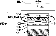
数据写入时,在中间层107(位线BL)中对应写入数据的电平流过其方向变化的数据写入电流±Iw。另一方面,沿着行方向配置的写入字线WWL中流过不管写入数据的电平如何都为一定方向的数据写入电流Ip。When writing data, data writing current ±Iw whose direction changes according to the level of the writing data flows in the intermediate layer 107 (bit line BL). On the other hand, the data writing current Ip flows in the writing word line WWL arranged along the row direction in a constant direction regardless of the level of the writing data.
对于自由磁化层103和104,通过流过中间层107(位线BL)的写入电流±Iw产生的数据写入磁场,施加易磁化轴(EA:Easy Axis)的磁场。与此相反,由流过写入字线WWL的数据写入电流Ip产生的数据写入磁场施加难磁化轴(HA:Hard Axis)的磁场。To the
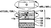
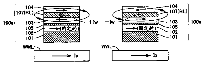
接着使用图4说明数据写入时的自由磁化层的磁化方向。图4A和图4B相当于图3的P-Q截面图。Next, the magnetization direction of the free magnetization layer during data writing will be described using FIG. 4 . 4A and 4B correspond to the P-Q sectional view of FIG. 3 .
参考图4A和4B,流过中间层107(位线BL)的数据写入电流±Iw的方向因写入数据的电平而异。Referring to FIGS. 4A and 4B, the direction of data write current ±Iw flowing through the intermediate layer 107 (bit line BL) varies depending on the level of write data.
图4A中,表示出中间层107(位线BL)中流过正方向的数据写入电流+Iw的情况。对应的写入字线WWL中也流过数据写入电流Ip时,自由磁化层103和104的磁化方向响应于数据写入电流+Iw产生的数据写入磁场而改换。FIG. 4A shows the case where the data write current +Iw in the forward direction flows through the intermediate layer 107 (bit line BL). When the data write current Ip also flows in the corresponding write word line WWL, the magnetization directions of the
此时,通过夹住非磁性的中间层107将自由磁化层103和104形成为层状,由于流过107中间层的数据写入电流产生的磁场可有效地将二者在彼此相反的方向上磁化为环状。一个自由磁化层的磁化产生的磁力线作为磁化另一个自由磁化层的磁力线,彼此相互作用。At this time, the
由此,可减小自由磁化层103和104的反转磁场强度产生所需的数据写入电流,由于磁力线不向外部扩张,因此可抑制对其他的存储器单元产生恶劣影响。As a result, the data write current required to generate the inversion magnetic field strength of the
另一方面,固定磁化层102的磁化方向固定到一定方向。因此,由数据写入电流+Iw进行数据写入的结果是固定磁化层102和自由磁化层103的磁化方向为相反方向,因此增大隧道磁电阻元件100a的电阻值。On the other hand, the magnetization direction of the fixed
另一方面,图4B中表示出中间层107(位线BL)中流过负方向的数据写入电流-Iw的情况。此时在与图4A的情况相反的方向上磁化自由磁化层103和104。流过写入字线WWL中的数据写入电流Ip如已经说明的那样不管写入数据的电平如何都保持一定方向。On the other hand, FIG. 4B shows the case where the data write current -Iw in the negative direction flows through the intermediate layer 107 (bit line BL). At this time, the
因此,通过数据写入电流-Iw执行数据写入的存储器单元中,固定磁化层102和自由磁化层103的磁化方向一致。其结果是隧道磁电阻元件100a的电阻值减小。Therefore, in the memory cell in which data writing is performed by the data writing current -Iw, the magnetization directions of the fixed
这样,仅对应的写入字线WWL和中间层107(位线BL)二者中流过数据写入电流的MTJ存储器单元中。决定自由磁化层103和104的材质和厚度,以使得自由磁化层103和104的磁化方向可改变,即执行数据写入。In this way, only the MTJ memory cells in which the data write current flows in both the corresponding write word line WWL and the intermediate layer 107 (bit line BL). The material and thickness of the
在根据实施例1的MTJ存储器单元中的隧道磁电阻元件中,与图51所示的已有隧道磁电阻元件不同,自由磁化层103和104的磁矩不需要有强弱。因此,自由磁化层103和104的每一个可用相同材质相等厚度形成。从而,可避免制造工序的复杂化。In the tunnel magneto-resistance element in the MTJ memory cell according to
再次参考图3,存取晶体管ATR包含作为P型衬底110上形成的n型区域的源/漏区域111和112、栅极113。源/漏区域111和接地电压VSS电耦合。Referring again to FIG. 3 , the access transistor ATR includes source/
属于相同的存储器单元行的MTJ存储器单元之间为使栅极113彼此电耦合,通过在行方向上延伸配置栅极113来配置读出字线RWL。即,响应读出字线RWL的激活(H电平)接通存取晶体管ATR。In order to electrically couple the
隧道磁电阻元件100a和存取晶体管ATR的源/漏区域112经势垒金属108和通路孔115电耦合。势垒金属108是用于对反铁磁体101电连接的缓冲部件。The
数据读出时,通过激活读出字线RWL(H电平)经隧道磁电阻元件100a的电阻将位线BL下拉到接地电压VSS。如已经说明的那样,对应自由磁化层103和固定磁化层102的磁化方向的相对关系改变隧道磁电阻元件100a的电阻值,因此对应MTJ存储器单元的存储数据,位线BL的电压变化举动不同。When reading data, the bit line BL is pulled down to the ground voltage VSS by activating the read word line RWL (H level) via the resistance of the
因此,位线BL中产生对应MTJ存储器单元MCa的存储数据电平的电压变化,使得通过检测流过传感电流时的位线BL的电压可读出MTJ存储器单元MCa的存储数据。Therefore, a voltage change corresponding to the stored data level of the MTJ memory cell MCa occurs in the bit line BL, so that the stored data of the MTJ memory cell MCa can be read out by detecting the voltage of the bit line BL when the sense current flows.
如上那样,自由磁化层104设置来在数据写入时与自由磁化层103一起磁化为环状,但数据写入时和数据读出时,电气上不起任何作用。因此,自由磁化层104如图3所示可配置为每个MTJ存储器单元的独立的元件,也可按与位线BL同样的图形配置为条状。As described above, the
通过这种结构,在图2所示的存储器阵列中,通过在与选择存储器单元对应的写入字线WWL和位线BL的每一个中流过数据写入电流,并且数据读出时,激活与选择存储器单元对应的写入字线RWL的同时检测位线BL的电压,可执行数据写入和数据读出。With this structure, in the memory array shown in FIG. 2, by flowing a data write current in each of the write word line WWL and the bit line BL corresponding to the selected memory cell, and when data is read, the activation and Data writing and data reading can be performed by detecting the voltage of the bit line BL while selecting the writing word line RWL corresponding to the memory cell.
图5表示具有2层存储节点构造的MTJ存储器单元的其他结构例。FIG. 5 shows another structural example of an MTJ memory cell having a two-layer memory node structure.
参考图5,具有2层存储节点构造的MTJ存储器单元MCb与图3所示的MTJ存储器单元MCa相比,不同点在于写入字线WWL配置得比隧道磁电阻元件100a和位线BL更上层。其他部分的结构与图3同样,因此不反复详细说明。从而对存储器单元MCh的数据写入和数据读出与存储器单元MCa同样执行。Referring to FIG. 5, the MTJ memory cell MCb having a two-layer storage node structure is different from the MTJ memory cell MCa shown in FIG. . The structure of other parts is the same as that in Fig. 3, so detailed description will not be repeated. Therefore, data writing and data reading to memory cell MCh are performed in the same manner as memory cell MCa.
通过这种结构,隧道磁电阻元件100a和存取晶体管ATR之间不需要设置布线层,因此二者的距离可缩短。其结果是通路孔115的宽高比(纵/横尺寸比)可减小,从而容易形成通路孔115,可简化制造工序。With this structure, no wiring layer is required between the
图6表示存储器阵列10的其他结构例。图6的结构中,可采用图2和图5分别示出的MTJ存储器单元MCa和MCb中的任何一个。FIG. 6 shows another configuration example of the
参考图6,对应各存储器单元列配置位线对。位线对BLP由2根互补位线构成。图6中,代表性示出第1列和第m列的位线对BLP1和BLPm。位线对BLP1包括位线BL1和/BL1,位线对BLPm包括位线BLm和/BLm。下面将位线对BLP1~BLPm统称为位线对BLP。同样,将位线/BL1~/BLm统称为位线/BL。位线BL和/BL使用中间层107形成。Referring to FIG. 6, bit line pairs are arranged corresponding to each memory cell column. The bit line pair BLP consists of two complementary bit lines. In FIG. 6 , the bit line pair BLP1 and BLPm of the first column and the m-th column are representatively shown. The bit line pair BLP1 includes bit lines BL1 and /BL1, and the bit line pair BLPm includes bit lines BLm and /BLm. Hereinafter, the bit line pairs BLP1 to BLPm are collectively referred to as the bit line pair BLP. Likewise, bit lines /BL1 to /BLm are collectively referred to as bit lines /BL. The bit lines BL and /BL are formed using the
MTJ存储器单元每一行与位线BL和/BL中的一个耦合。例如,就属于第1列的存储器单元作说明,则第1行的存储器单元与位线BL耦合,第2行的存储器单元与位线/BL耦合。下面同样,各个存储器单元在奇数行中与位线对的一方BL1~BLm连接,在偶数行中与位线对的另一方/BL1~/BLm连接。其结果是读出字线RWL对应行选择结果被选择地激活时,位线对的一方BL1~BLm和位线对的另一方/BL1~/BLm中的一个与存储器单元耦合。Each row of MTJ memory cells is coupled to one of bit lines BL and /BL. For example, regarding the memory cells belonging to the first column, the memory cells of the first row are coupled to the bit line BL, and the memory cells of the second row are coupled to the bit line /BL. Similarly, each memory cell is connected to one of the bit line pairs BL1 to BLm in the odd-numbered rows, and connected to the other one of the bit line pairs /BL1 to /BLm in the even-numbered rows. As a result, when the read word line RWL is selectively activated in response to the row selection result, one of the bit line pair BL1 to BLm and the other bit line pair /BL1 to /BLm is coupled to the memory cell.
列解码器25对应列地址CA的解码结果将分别对应存储器单元列的列选择信号YS1~Ysm中的一个激活为选择状态(H电平)。传送读出数据和写入数据的数据总线对DBP具有互补的数据总线DB和/DB。The
读出/写入控制电路50包含列选择栅CSG1~CSGm、数据写入电路51W和数据读出电路51R。The read/
列选择栅CSG1~CSGm分别配置在位线对BLP1~BLPm和数据总线对DBP之间。列选择栅CSG1~CSGm的每一个包含电耦合在数据总线DB和对应的位线BL之间的晶体管开关、电耦合在数据总线/DB和对应的位线/BL之间的晶体管开关。这些晶体管开关响应对应的列选择信号的激活而导通。Column selection gates CSG1 to CSGm are arranged between the pair of bit lines BLP1 to BLPm and the pair of data buses DBP, respectively. Each of the column select gates CSG1-CSGm includes a transistor switch electrically coupled between the data bus DB and the corresponding bit line BL, a transistor switch electrically coupled between the data bus /DB and the corresponding bit line /BL. These transistor switches are turned on in response to activation of corresponding column select signals.
例如,列选择栅CSG1包含电耦合在数据总线DB和位线BL1之间响应列选择信号YS1的激活而导通的晶体管开关、电耦合在数据总线/DB和对应的位线/BL1之间响应列选择信号YS1的激活而接通的的晶体管开关。For example, column select gate CSG1 includes a transistor switch electrically coupled between data bus DB and bit line BL1 that turns on in response to activation of column select signal YS1, and electrically coupled between data bus /DB and corresponding bit line /BL1 in response to activation of column select signal YS1. The activation of the column select signal YS1 turns on the transistor switch.
分别对应位线对BLP1~BLPm来分别设置用于电耦合对应的互补位线之间的短路晶体管EQT1~EQTm和控制信号EQS1~EQSm。控制信号EQS1~EQSm在数据写入时在对应的存储器单元列被选择为数据写入对象的情况下被激活H电平。下面统称短路晶体管EQT1~EQTm为短路晶体管EQT。The short-circuit transistors EQT1-EQTm and the control signals EQS1-EQSm for electrically coupling between the corresponding complementary bit lines are provided respectively corresponding to the bit line pairs BLP1-BLPm. The control signals EQS1 to EQSm are activated at the H level when the corresponding memory cell column is selected as a data writing target at the time of data writing. Hereinafter, short-circuit transistors EQT1 to EQTm are collectively referred to as short-circuit transistors EQT.
各短路晶体管EQT在控制信号EQS1~EQSm的对应的一个被激活为H电平时,电耦合对应的位线BL和/BL。或者,替代各个控制信号EQS1~EQSm,在数据写入时使用被激活(H电平)的控制信号WE。Each short-circuit transistor EQT is electrically coupled to the corresponding bit line BL and /BL when a corresponding one of the control signals EQS1 to EQSm is activated at the H level. Alternatively, instead of the respective control signals EQS1 to EQSm, the control signal WE that is activated (H level) is used at the time of data writing.
数据写入电路51W在数据写入时对应写入数据DIN将数据总线DB和/DB分别设定到电源电压VDD和接地电压VSS之一。另外,数据写入时,至少选择存储器单元列中,短路晶体管EQT接通,因此对应由数据写入电路51W设定的数据总线DB和/DB的电压差,将数据写入电流流过选择的存储器单元列的位线BL和/BL,将其作为往返电流。另一方面,与选择的存储器单元行对应的写入字线WWL中提供不依赖于写入数据的电平的一定方向的数据写入电流Ip。Data write
根据这种结构,数据写入时,仅通过对应写入数据DIN的电平改换数据总线DB和/DB的电压设定就可容易地控制流过位线BL(/BL)的数据写入电流±Iw的方向。即,可简化数据写入电路51W的结构。According to this structure, the data writing current flowing through the bit line BL (/BL) can be easily controlled only by changing the voltage setting of the data bus line DB and /DB according to the level of the writing data DIN during data writing. The direction of ±Iw. That is, the configuration of the
接着说明数据读出动作。Next, the data read operation will be described.
数据读出时,经对应的位线BL或/BL和选择存储器单元中的隧道磁电阻元件100a将数据总线DB和/DB之一下拉到接地电压VSS。其结果是和选择存储器单元连接的数据总线DB或/DB上产生对应选择存储器单元的存储数据电平的电压变化。数据读出线路51R对应数据总线DB和/DB的电压生成读出数据DOUT。When reading data, one of the data bus lines DB and /DB is pulled down to the ground voltage VSS via the corresponding bit line BL or /BL and the
或者,在存储器阵列10中配置具有MTJ存储器单元的电阻值R0和R1的中间值的伪存储器单元(未示出),在数据读出时,在数据总线DB和/DB上连接选择存储器单元和伪存储器单元之一。此时,数据读出线路51R根据数据总线DB和/DB的电压比较执行互补型的数据读出,提高动作裕度。Alternatively, a dummy memory cell (not shown) having an intermediate value of the resistance values R0 and R1 of the MTJ memory cell is arranged in the
图7表示存储器阵列10的另一结构例。FIG. 7 shows another configuration example of the
图7所示的结构中,具有2层存储节点构造的存储器单元MCc配置为n行×m列。另外,数据写入用的写入位线WBL和数据读出用的读出位线RBL分割配置。另一方面,省略源线SL的配置。In the structure shown in FIG. 7, memory cells MCc having a two-layer storage node structure are arranged in n rows×m columns. In addition, the write bit line WBL for writing data and the read bit line RBL for reading data are arranged separately. On the other hand, the arrangement of the source line SL is omitted.
写入位线WBL和读出位线RBL分别对应存储器单元列配置。图7中,代表性示出对应第1列和第m列的写入位线WBL1,WBLm和读出位线RBL1,RBLm。统称读出位线RBL1~RBLm时以及统称写入位线WBL1~WBLm时分别使用符号RBL和WBL。The write bit lines WBL and the read bit lines RBL are respectively arranged corresponding to memory cell columns. In FIG. 7, write bit lines WBL1, WBLm and read bit lines RBL1, RBLm corresponding to the first column and the m-th column are representatively shown. When collectively referring to read bit lines RBL1 to RBLm and collectively referring to write bit lines WBL1 to WBLm, symbols RBL and WBL are used, respectively.
参考图8,具有图7所示的2层存储节点构造的MTJ存储器单元MCc与图5所示的MTJ存储器单元MCa相比,不同点是还配置在列方向上延伸设置的读出位线RBL。Referring to FIG. 8 , the MTJ memory cell MCc having the two-layer storage node structure shown in FIG. 7 differs from the MTJ memory cell MCa shown in FIG. 5 in that a read bit line RBL extending in the column direction is further arranged. .
使用中间层107形成写入位线WBL。写入位线WBL上在数据写入时流过数据写入电流±Iw。另一方面,在数据读出时通过读出/写入控制电路50,60将各写入位线WBL设定到接地电位VSS。Write bit line WBL is formed using
读出位线RBL经通路孔116电耦合于存取晶体管ATR的源/漏区域111。数据读出时源/漏区域112用作存取晶体管ATR的源区。The read bit line RBL is electrically coupled to the source/
其结果是响应于存取晶体管ATR的接通,在读出位线RBL~存取晶体管ATR~隧道磁电阻元件100a~写入位线WBL(接地电位VSS)中形成传感电流路径。As a result, in response to turning on of access transistor ATR, a sense current path is formed from read bit line RBL to access transistor ATR to
再次参考图7,通过在与选择存储器单元对应的写入字线WWL和读出位线WBL中分别流过数据写入电流Ip和±Iw执行数据写入。Referring again to FIG. 7 , data writing is performed by flowing data writing currents Ip and ±Iw in the writing word line WWL and the reading bit line WBL corresponding to the selected memory cell, respectively.
数据读出时,响应与选择存储器单元对应的读出字线RWL的激活经选择存储器单元中的隧道磁电阻元件100a可将与选择存储器单元对应的读出位线RBL下拉到接地电位VSS。其结果是在读出位线RBL上产生对应选择存储器单元的存储数据的电平的典雅变化,从而可读出选择存储器单元的存储数据。During data reading, in response to activation of the read word line RWL corresponding to the selected memory cell, the tunnel magneto-
图9表示具有2层存储节点构造的MTJ存储器单元的其他结构例。FIG. 9 shows another structural example of an MTJ memory cell having a two-layer memory node structure.
参考图9,MTJ存储器单元MCd与图5所示的MTJ存储器单元MCb相比,不同点在于不在中间层107中形成位线BL而设置与位线BL独立的金属布线层。Referring to FIG. 9 , MTJ memory cell MCd differs from MTJ memory cell MCb shown in FIG. 5 in that bit line BL is not formed in
即图9的结构中,中间层107固定在固定电压,如接地电压VSS。其结果是不需要考虑MTJ存储器单元之间的电干扰,因此可将中间层107作成平面状或条状的任何形状。即中间层107的形状自由度提高,故得到的效果是制造过程简易,成品率提高。That is, in the structure of FIG. 9 , the
位线BL在列方向上延伸配置,经通路孔116电耦合于源/漏区域111。另一方面,存取晶体管ATR的源/漏区域112经通路孔115和势垒金属108电耦合于隧道磁电阻元件100a。The bit line BL is arranged to extend in the column direction, and is electrically coupled to the source/
数据写入时,位线BL和写入字线WWL上分别流过数据写入电流±Iw和Ip,使得可将自由磁化层113和114磁化到与写入数据DIN对应的方向上。在MTJ存储器单元MCd中,为使自由磁化层113和114的磁矩(磁化阈值)有强弱,可用不同材质和厚度分别制作。During data writing, data writing currents ±Iw and Ip respectively flow through the bit line BL and the writing word line WWL, so that the
数据读出时,通过激活读出字线RWL,经隧道磁电阻元件100a的电阻将位线BL下拉到接地电位VSS。其结果是位线BL上产生对应隧道磁电阻元件的电阻值,即MTJ存储器单元的存储数据电平的电压变化,从而可读出选择存储器单元的存储数据。When reading data, by activating the read word line RWL, the bit line BL is pulled down to the ground potential VSS via the resistance of the
这样根据实施例1的2层存储节点构造的MTJ存储器单元,即便在缩小存储器单元尺寸的情况下,也可抑制产生反转磁场强度的数据写入电流量的增大,从而容易缩小(scaling)存储器单元。Thus, according to the MTJ memory cell with the two-layer storage node structure of
对于相同尺寸的存储器单元,由于可抑制产生反转磁场强度的数据写入电流量,因此可降低功耗。尤其,在2层自由磁化层夹住的中间层中流过数据写入电流,可有效地得到反转磁场强度,从而用更小的数据写入电流即可进行数据写入,进一步降低消耗电流。For a memory cell of the same size, since the amount of data writing current that generates a reversal magnetic field strength can be suppressed, power consumption can be reduced. In particular, the data writing current can be effectively obtained by flowing the data writing current in the intermediate layer sandwiched by the two free magnetization layers, so that the strength of the reverse magnetic field can be effectively obtained, so that data writing can be performed with a smaller data writing current, further reducing current consumption.
由于使用隧道磁电阻元件内的中间层来形成位线,因此可减少需要的金属布线层的数目。这样,尤其在MRAM器件和逻辑电路等上混装来构成系统在芯片上器件时,在MRAM阵列尚不区域中可使用的金属布线层的数目可增加,从而逻辑电路的设计自由度增加,可减少芯片尺寸。Since bit lines are formed using intermediate layers within the tunnel magnetoresistive element, the number of required metal wiring layers can be reduced. In this way, especially when an MRAM device and a logic circuit are mixed to form a system-on-chip device, the number of metal wiring layers that can be used in an area of the MRAM array can be increased, thereby increasing the degree of freedom in the design of the logic circuit. Reduce chip size.
实施例2Example 2
实施例1中,说明了使用隧道磁电阻元件内的中间层来形成位线的结构。但是中间高才生的膜厚不能设计到很薄,因此在列方向上延伸中间层来配置位线BL时,其电阻值会比较大。因此数据读出速度降低,难以供给足够的数据写入电流。In
因此,实施例2中,对于配置实施例1说明的2层存储节点构造的MTJ存储器单元的存储器阵列,采用所谓的分层位线结构。Therefore, in the second embodiment, a so-called hierarchical bit line structure is adopted for the memory array in which the MTJ memory cells of the two-layer storage node structure described in the first embodiment are arranged.
参考图10,在根据实施例2的结构中,在存储器阵列10中分别对应存储器单元分层设置主位线MBL和子位线SBL。另外,分别对应存储器单元列配置主位线MBL和互补的主位线/MBL和子位线SBL和互补的子位线/SBL。子位线SBL和/SBL与图3和图5所示的位线BL一样,使用隧道磁电阻元件100a的中间层107来形成。另一方面,主位线MBL和/MBL使用电阻小的独立的金属布线形成。主位线MBL和/MBL构成主位线对MBLP,子位线SBL和/SBL构成子位线对SBLP。Referring to FIG. 10, in the structure according to Embodiment 2, main bit lines MBL and sub bit lines SBL are hierarchically arranged in
图10中,代表性表示出第1列和第m列的主位线MBL1和/MBL1以及MBLm和/MBLm。主位线MBL1和/MBL1构成主位线对MBLP。下面分别统称主位线MBL1~MBLm和/MBL1~/MBLm时,简称为主位线MBL和/MBL。统称主位线对MBLP1~MBLPm时简称为主位线对MBLP。In FIG. 10 , main bit lines MBL1 and /MBL1 and MBLm and /MBLm of the first column and the m-th column are representatively shown. Main bit lines MBL1 and /MBL1 constitute a main bit line pair MBLP. When the main bit lines MBL1-MBLm and /MBL1-/MBLm are collectively referred to below, they are referred to as main bit lines MBL and /MBL for short. When collectively referred to as the master bit line pair MBLP1-MBLPm, it is simply referred to as the master bit line pair MBLP.
读出/写入控制电路50用作为对与选择的存储器单元列对应的主位线MBL和/MBL提供数据写入电流±Iw的供给源。例如,读出/写入控制电路50具有和图6相同的结构,对应写入数据DIN的数据电平将与选择的存储器单元列对应的主位线MBL和/MBL分别耦合于电源电压VDD和接地电压VSS。The read/
各存储器单元列沿着行方向被分割为k个存储器块。例如,属于第1列的MTJ存储器单元全分割为存储器块MBa11~MBak1,同样属于第m列的MTJ存储器单元全分割为存储器块MBa1m~MBakm。存储器阵列10整体中,存储器块MBa11~MBakm按k行×m列呈行列状配置。下面也称为存储器块MBa。Each column of memory cells is divided into k memory blocks along the row direction. For example, all MTJ memory cells belonging to the first column are divided into memory blocks MBa11 to MBak1 , and all MTJ memory cells belonging to the m-th column are all divided into memory blocks MBa1m to MBakm. In the
在各存储器单元列中,子位线SBL在每个存储器块MBa上配置。在各个存储器块MBa中,配置子位线SBL和互补的子位线/SBL。互补的子位线SBL和/SBL构成子位线对SBLP。例如,在存储器块MBa11中,配置构成子位线对SBLP11的子位线SBL11和/SBL11。In each memory cell column, a sub bit line SBL is arranged on each memory block MBa. In each memory block MBa, a sub bit line SBL and a complementary sub bit line /SBL are arranged. Complementary sub-bit lines SBL and /SBL constitute a sub-bit line pair SBLP. For example, in memory block MBa11, sub bit lines SBL11 and /SBL11 constituting sub bit line pair SBLP11 are arranged.
下面在分别统称子位线SBL11~SBLkm和/SBL11~/SBLkm的情况下,简单称为子位线SBL和/SBL。Hereinafter, sub-bit lines SBL11 to SBLkm and /SBL11 to /SBLkm are collectively referred to as sub-bit lines SBL and /SBL for short.
块选择信号BS1~BSk分别对应存储器块的行设置。统称块选择信号BS1~BSk,则简称为块选择信号BS。块选择信号BS在包含选择存储器单元的存储器块的行中被激活。The block selection signals BS1˜BSk are respectively set corresponding to the rows of the memory block. They are collectively referred to as the block selection signals BS1˜BSk, and are simply referred to as the block selection signal BS. The block select signal BS is activated in a row of a memory block containing selected memory cells.
即,通过块选择信号BS和存储器单元列(主位线对MBLP)的选择可选择包含选择存储器单元的特定的存储器块。That is, a specific memory block including the selected memory cells can be selected by the block selection signal BS and the selection of the memory cell column (main bit line pair MBLP).
图11是表示存储器块MBa的结构的电路图。各存储器块MBa的结构相同,因此图11中代表性表示出存储器块MBa11的结构。存储器块MBa11中配置子位线SBL11和/SBL11。FIG. 11 is a circuit diagram showing the configuration of the memory block MBa. Since the structures of the memory blocks MBa are the same, FIG. 11 typically shows the structure of the memory block MBa11. Sub bit lines SBL11 and /SBL11 are arranged in memory block MBa11.
参考图11,在存储器块MBa11中配置多行(例如3行)×1列的存储器单元群。Referring to FIG. 11 , memory cell groups of a plurality of rows (for example, 3 rows)×1 column are arranged in a memory block MBa11.
下面在实施例2及其变形例中,表示出各存储器块中包含的存储器单元行的数目为3个的结构例,但本发明的适用不限于此,与各存储器块对应的存储器单元行的数目可为任意的多个。In Embodiment 2 and its modified examples below, a structural example in which the number of memory cell rows included in each memory block is three is shown, but the application of the present invention is not limited to this, and the number of memory cell rows corresponding to each memory block The number can be any number.
与图6所示结构相同,在各存储器单元列中,MTJ存储器单元MCa每一行连接子位线SBL11和/SBL11之一。例如,与奇数行对应的MTJ存储器单元MCa耦合子位线SBL11,与偶数行对应的MTJ存储器单元MCa耦合子位线/SBL11。In the same structure as shown in FIG. 6, in each memory cell column, the MTJ memory cell MCa is connected to one of sub-bit lines SBL11 and /SBL11 per row. For example, MTJ memory cells MCa corresponding to odd-numbered rows are coupled to sub-bit line SBL11, and MTJ memory cells MCa corresponding to even-numbered rows are coupled to sub-bit line /SBL11.
下面对于实施例2及其变形例,表示出各存储器块中配置MTJ存储器单元MCa的结构的例子,但可替代MTJ存储器单元MCa来采用图5和图9所示的MTJ存储器单元MCb和MCd。An example of the structure in which MTJ memory cell MCa is arranged in each memory block is shown below for Embodiment 2 and its modification, but MTJ memory cells MCb and MCd shown in FIGS. 5 and 9 may be used instead of MTJ memory cell MCa.
MTJ存储器单元MCa包含存取晶体管ATR和隧道磁电阻元件100a。存取晶体管ATR电耦合在隧道磁电阻元件100a和接地电压VSS之间。存取晶体管ATR的栅上耦合对应的存储器单元行的读出字线RWL。The MTJ memory cell MCa includes an access transistor ATR and a
子位线SBL11和/SBL11的每一个对每个存储器块MBa分割,因此布线缩短。其结果是使用隧道磁电阻元件100a的中间层107形成的各子位线SBL的电阻值可被抑制。Each of the sub-bit lines SBL11 and /SBL11 is divided for each memory block MBa, so wiring is shortened. As a result, the resistance value of each sub-bit line SBL formed using the
存储器块MBa11还包含电流开关晶体管SWTa和SWTb以及短路晶体管EQT11。The memory block MBal1 also includes current switch transistors SWTa and SWTb and a short-circuit transistor EQT11.
电流开关晶体管SWTa电耦合在主位线MBL1和子位线SBL11的一端(靠近读出/写入控制电路50的一侧)之间。同样,电流开关晶体管SWTb电耦合在主位线/MBL1和子位线/SBL11的一端(靠近读出/写入控制电路50的一侧)之间。电流开关晶体管SWTa和SWTb的每一个的栅上输入块选择信号BS1。The current switch transistor SWTa is electrically coupled between the main bit line MBL1 and one end of the sub bit line SBL11 (the side closer to the read/write control circuit 50 ). Also, the current switch transistor SWTb is electrically coupled between the main bit line /MBL1 and one end of the sub bit line /SBL11 (the side closer to the read/write control circuit 50). A block selection signal BS1 is input to a gate of each of the current switching transistors SWTa and SWTb.
短路晶体管EQT11响应写入选择信号WMB11电耦合子位线SBL11和/SBL11的另一端(远离读出/写入控制电路50的一侧)。The short-circuit transistor EQT11 is electrically coupled to the other end of the sub-bit line SBL11 and /SBL11 (the side away from the read/write control circuit 50 ) in response to the write select signal WMB11 .
写入选择信号WMB11至少在数据写入时在块选择信号BS1被激活的情况下激活为H电平。或者,除列选择结果外,在数据写入时,激活块选择信号BS1并且选择与主位线对MBLp1对应的存储器单元列的情况下,被激活为H电平。Write selection signal WMB11 is activated at H level at least when block selection signal BS1 is activated during data writing. Alternatively, block selection signal BS1 is activated at the H level when the memory cell column corresponding to the main bit line pair MBLp1 is selected during data writing in addition to the column selection result.
存储器块MBa11成为数据写入对象时,短路晶体管EQT11和电流开关晶体管SWTa和SWTb的每一个都被接通。其结果是通过读出/写入控制电路50切换主位线MBL1和/MBL1的电压极性(电源电压VDD和接地电压VSS),在子位线SBL11和/SBL11中流过对应写入数据DIN的电平的方向的数据写入电流±Iw,作为由短路晶体管EQT11折返的往返电流。因此,可简化作为数据写入电流±Iw的供给源的读出/写入控制电路50的结构。When the memory block MBa11 becomes a data writing target, each of the short-circuit transistor EQT11 and the current switch transistors SWTa and SWTb is turned on. As a result, the voltage polarities (power supply voltage VDD and ground voltage VSS) of the main bit lines MBL1 and /MBL1 are switched by the read/
另外,选择地激活与选择存储器单元对应的写入字线WWL,接受数据写入电流Ip的供给。由此,也对选择存储器单元写入写入数据DIN。Also, the write word line WWL corresponding to the selected memory cell is selectively activated to receive the supply of the data write current Ip. Accordingly, the write data DIN is also written in the selected memory cell.
另一方面,存储器块MBa11被选择为数据读出对象的情况下,电流开关晶体管SWTa和SWTb导通,而短路晶体管EQT11断开。由此,子位线SBL11和/SBL11分别电耦合主位线MBL1和/MBL1。On the other hand, when the memory block MBa11 is selected as a data read target, the current switch transistors SWTa and SWTb are turned on, and the short-circuit transistor EQT11 is turned off. Thus, sub bit lines SBL11 and /SBL11 are electrically coupled to main bit lines MBL1 and /MBL1, respectively.
根据实施例2的结构中,执行使用了伪存储器单元DMC的所谓的互补型的数据读出。互补型的数据读出执行用的伪存储器单元DMC对应主位线MBL和/MBL的每一个配置。图11中代表性表示出对应主位线MBL1设置的伪存储器单元和对应主位线/MBL1设置的伪存储器单元。In the configuration according to the second embodiment, so-called complementary data reading using dummy memory cells DMC is performed. Dummy memory cells DMC for performing complementary data reading correspond to each arrangement of main bit lines MBL and /MBL. FIG. 11 typically shows a dummy memory cell corresponding to main bit line MBL1 and a dummy memory cell corresponding to main bit line /MBL1.
伪存储器单元DMC的每一个具有存取晶体管ATR和伪电阻Rd。伪电阻Rd的电阻值设定在分别对应存储数据的电平1和0的MTJ存储器单元的电阻值R1和R0的中间值,即设定为R1<Rd<R0。Each of the dummy memory cells DMC has an access transistor ATR and a dummy resistor Rd. The resistance value of the dummy resistor Rd is set at the middle value of the resistance values R1 and R0 of the MTJ memory cells corresponding to the
对应主位线MBL1的伪存储器单元响应伪字线DWL0的激活而电耦合在接地电压VSS和主位线MBL1之间。另一方面,对应主位线/MBL1设置的伪存储器单元响应伪字线DWL1的激活而电耦合在主位线/MBL1和接地电压VSS之间。The dummy memory cells corresponding to the main bit line MBL1 are electrically coupled between the ground voltage VSS and the main bit line MBL1 in response to activation of the dummy word line DWL0. On the other hand, dummy memory cells disposed corresponding to the main bit line /MBL1 are electrically coupled between the main bit line /MBL1 and the ground voltage VSS in response to activation of the dummy word line DWL1.
伪字线DWL0和DWL1响应选择存储器单元属于奇数行还是偶数行被选择激活。即,选择存储器单元属于奇数行的情况下,也就是选择存储器单元电耦合主位线MBL1的情况下,由于将伪存储器单元DMC耦合于主位线/MBL1,伪字线DWL1被激活。相反,选择存储器单元属于偶数行的情况下,由于将伪存储器单元DMC耦合于主位线MBL1,伪字线DWL0被激活。The dummy word lines DWL0 and DWL1 are selectively activated in response to selecting whether the memory cell belongs to an odd row or an even row. That is, when the selected memory cell belongs to an odd row, that is, the selected memory cell is electrically coupled to the main bit line MBL1, the dummy word line DWL1 is activated by coupling the dummy memory cell DMC to the main bit line /MBL1. On the contrary, when the selected memory cell belongs to an even row, the dummy word line DWL0 is activated by coupling the dummy memory cell DMC to the main bit line MBL1.
由此,数据读出时,互补的主位线MBL1和/MBL1上电耦合选择存储器单元和伪存储器单元DMC之一。因此,通过检测主位线MBL1和/MBL1的电压差可读出选择存储器单元的存储数据。Therefore, when data is read, the complementary main bit lines MBL1 and /MBL1 are electrically coupled to select one of the memory cell and the dummy memory cell DMC. Therefore, the stored data of the selected memory cell can be read out by detecting the voltage difference between the main bit lines MBL1 and /MBL1.
各子位线SBL,/SBL的布线缩短,其电阻值减小,因此使用根据实施例1的2层存储节点构造的MTJ存储器单元实现数据写入时功耗减少的结构也不会导致数据读出的速度降低。The wiring of each sub-bit line SBL, /SBL is shortened, and its resistance value is reduced. Therefore, the structure of reducing power consumption during data writing by using the MTJ memory cell of the 2-layer storage node structure according to
实施例2的变形例1
实施例2的变形例1中,说明可执行有效的数据写入电流供给的分层子位线结构。In
参考图12,在根据实施例2的变形例1的结构中,图10所示的存储器阵列10的结构中,替代存储器块MBa11~MBakm而配置存储器块MBb11~MBbkm。存储器块MBb11~MBbkm的每一个具有相同结构,因此图12中代表性示出存储器块MBb11的结构。Referring to FIG. 12 , in the configuration according to
存储器块MBb11与图11所示的存储器块MBa11相比,不同点是更换短路晶体管EQT11和电流开关晶体管SWTa,SWTb的配置位置。The memory block MBb11 differs from the memory block MBa11 shown in FIG. 11 in that the arrangement positions of the short-circuit transistor EQT11 and the current switch transistors SWTa and SWTb are replaced.
存储器块MBb11中,短路晶体管EQT11连接靠近子位线SBL11和/SBL11的读出控制电路50的一端之间。同样,电流开关晶体管SWTa电耦合在远离子位线SBL11的读出控制电路50的另一端和主位线MBL1之间,电流开关晶体管SWTb电耦合在子位线/SBL11的另一端(远离读出控制电路50侧)和主位线/MBL1之间。In memory block MBb11, short-circuit transistor EQT11 is connected between one end of
通过这种结构,在数据写入时,数据写入电流±Iw按彼此相反方向分别流向主位线MBL1和子位线SBL11。同样,在主位线/MBL1和子位线/SBL11之间也流过彼此相反方向的数据写入电流±Iw。With this structure, at the time of data writing, data writing currents ±Iw flow to main bit line MBL1 and sub bit line SBL11 in directions opposite to each other. Similarly, data write currents ±Iw in opposite directions also flow between main bit line /MBL1 and sub bit line /SBL11.
接着图13A和13B说明根据实施例2的变形例1的存储器块的数据写入磁场产生状态。Next, FIGS. 13A and 13B explain the data writing magnetic field generation state of the memory block according to
图13A中表示出子位线SBL(/SBL)上流过正方向的数据写入电流+Iw时的数据写入磁场状态。此时,主位线MBL(/MBL)上在反方向上流过数据写入电流,因此通过分别流过子位线SBL(/SBL)和主位线MBL(/MBL)的数据写入电流产生的数据写入磁场在自由磁化层104中彼此强烈耦合。由于自由磁化层104的磁化产生的磁力线用作磁化另一自由磁化层103的磁力线,因此通过更小的数据写入电流产生反转磁场强度。FIG. 13A shows the state of the data write magnetic field when the data write current +Iw in the positive direction flows through the sub-bit line SBL (/SBL). At this time, the data write current flows in the reverse direction on the main bit line MBL (/MBL), so the data write currents flowing through the sub bit line SBL (/SBL) and main bit line MBL (/MBL) respectively generate The data writing magnetic fields of 2 are strongly coupled to each other in the
图13B中表示出对子位线SBL(/SBL)上流过负方向的数据写入电流-Iw时的数据写入磁场状态。此时,与图13A相同,作用于自由磁化层104的数据写入磁场彼此强烈耦合,因此通过更小的数据写入电流可执行对MTJ存储器单元的数据写入。FIG. 13B shows the state of the data write magnetic field when the data write current -Iw in the negative direction flows to the sub bit line SBL (/SBL). At this time, as in FIG. 13A, the data writing magnetic fields acting on the
再次参考图12,存储器块MBb11的其他部分的结构与图11所示的存储器块MBa11相同,因此不反复其详细说明。即,根据实施例2的变形例1的结构的数据读出动作与根据实施例2的存储器块MBa同样执行。Referring again to FIG. 12 , the structure of other portions of the memory block MBb11 is the same as that of the memory block MBa11 shown in FIG. 11 , and thus detailed description thereof will not be repeated. That is, the data reading operation according to the configuration of the
实施例2的变形例2Modification 2 of Embodiment 2
实施例2的变形例2中,说明对多个存储器单元列的每一个配置主位线的结构。In Modification 2 of Embodiment 2, a configuration in which a main bit line is arranged for each of a plurality of memory cell columns will be described.
参考图14,在根据实施例2的变形例2的结构的存储器阵列的结构中,在按行列状布置的存储器块MBb11~MBbkm的每一个中独立设置构成子位线对SBLP的子位线SBL和/SBL。各主位线对MBLP对多个存储器单元列的每一个配置。图12中作为一例表示出对2个存储器单元列的每一个配置主位线对MBLP的结构。因此,在存储器阵列10整体中,配置h个(h∶h=m/2的整数)的主位线对MBLP1~MBLPh。伪存储器单元DMC对于各主位线MBL的配置与图11相同,因此不作详细说明。Referring to FIG. 14 , in the structure of the memory array according to the structure of Modification 2 of Embodiment 2, the sub-bit lines SBL constituting the sub-bit line pair SBLP are independently provided in each of the memory blocks MBb11 to MBbkm arranged in a matrix. and /SBL. Each main bit line pair MBLP is arranged for each of a plurality of memory cell columns. FIG. 12 shows an example in which a main bit line pair MBLP is arranged for each of two memory cell columns. Therefore, h (h:h=an integer of m/2) main bit line pairs MBLP1 to MBLPh are arranged in the
主位线对MBLP1为存储器块MBb11~MBbk1和MBb12~MBbk2共有。The main bit line pair MBLP1 is shared by the memory blocks MBb11 to MBbk1 and MBb12 to MBbk2.
图12中输入电流开关晶体管SWTa和SWTb的栅的块选择信号BS1为在与相同的主位线对应的多个存储器单元之间进行选择而进行细分。The block selection signal BS1 input to the gates of the current switching transistors SWTa and SWTb in FIG. 12 is subdivided for selecting among a plurality of memory cells corresponding to the same main bit line.
图14的结构中,块选择信号BS1分为块选择信号BS1A和BS1B。块选择信号BS1A在选择第1行的存储器块并且选择存储器单元属于奇数列时被激活。另一方面,块选择信号BS1B在选择第1行的存储器块并且选择存储器单元属于偶数列时被激活。即,与相同的存储器块的行对应的块选择信号BS1A和BS1B对应选择存储器单元属于偶数列还是奇数列激活其中一个。In the structure of FIG. 14, block selection signal BS1 is divided into block selection signals BS1A and BS1B. The block selection signal BS1A is activated when a memory block of the first row is selected and memory cells belonging to odd columns are selected. On the other hand, the block selection signal BS1B is activated when the memory block of the first row is selected and the selected memory cells belong to the even columns. That is, the block selection signals BS1A and BS1B corresponding to the row of the same memory block correspondingly select whether the memory cell belongs to an even column or an odd column and activate one of them.
对存储器块MBa11~MBak1分别传送块选择信号BS1A~BskA,对存储器块MBa12~MBak2分别传送块选择信号BS1B~BSkB。通过组合主位线对MBP的选择和块选择信号BS1A,BS1B~BskA,BSkB,可指定包含选择存储器单元的存储器块。Block selection signals BS1A to BskA are transmitted to the memory blocks MBa11 to MBak1, respectively, and block selection signals BS1B to BSkB are transmitted to the memory blocks MBal2 to MBak2, respectively. By combining the selection of the master bit line pair MBP and the block selection signals BS1A, BS1B-BskA, BSkB, a memory block including selected memory cells can be designated.
通过这种结构,在存储器阵列10整体中,可减少主位线的配置根数。其结果是确保主位线的布线间距。With this configuration, the number of master bit lines arranged in the
由此,数据写入时流过比较大的电流的主位线的布线宽度,即截面面积可充分确保,降低电流密度。因此抑制主位线的电迁移现象等产生。提高MRAM器件的动作可靠性。As a result, the wiring width of the main bit line through which relatively large current flows during data writing, that is, the cross-sectional area can be sufficiently ensured, and the current density can be reduced. Therefore, the occurrence of electromigration phenomenon and the like on the main bit line is suppressed. The operation reliability of the MRAM device is improved.
另外,随着减少主位线的配置根数,可减少伪存储器单元的配置个数,从而可实现芯片面积的减少。In addition, as the number of arranged main bit lines is reduced, the number of arranged dummy memory cells can be reduced, thereby reducing the chip area.
实施例2的变形例3Modification 3 of Embodiment 2
在实施例2以后的变形例中,说明各存储器块具有开放位线结构的情况。In the modified examples after the second embodiment, the case where each memory block has an open bit line structure will be described.
参考图15,根据实施例2的变形例3的存储器阵列10中,存储器块MBc11~MBckh按k行×h列呈行列状配置。存储器块MBc11~MBckh的每一个包含2个存储器单元列。因此,存储器单元行和存储器单元列数若与实施例2相同,则存储器块的个数为实施例2的一半。下面统称存储器块MBc11~MBchk,将其简称存储器块MBc。Referring to FIG. 15 , in the
主位线MBL1~MBLm分别对应存储器单元列设置。即,各存储器块MBc对应成对的2根主位线MBL。The main bit lines MBL1 ˜ MBLm are arranged corresponding to memory cell columns, respectively. That is, each memory block MBc corresponds to a pair of two main bit lines MBL.
除与图10相同的块选择信号BS1~BSk,设置写入选择信号WMB1A,WMB1B~WMBkA,WMBkB。写入选择信号WMB1A,WMB1B~WMBkA,WMBkB对应选择存储器单元属于的存储器块的行和选择存储器单元属于奇数列还是偶数列被选择地激活。例如,写入选择信号WMB1A在选择存储器单元属于第1行的存储器块的行并且属于奇数列的情况下被激活。同样,写入选择信号WMB1B在选择存储器单元属于第1行的存储器块的行并且属于偶数列的情况下被激活。In addition to the same block selection signals BS1 to BSk as in FIG. 10, write selection signals WMB1A, WMB1B to WMBkA, WMBkB are set. The write selection signals WMB1A, WMB1B˜WMBkA, WMBkB are selectively activated corresponding to the row of the memory block to which the selected memory cell belongs and whether the selected memory cell belongs to an odd-numbered column or an even-numbered column. For example, the write selection signal WMB1A is activated when the selected memory cell belongs to the row of the memory block of the first row and belongs to an odd column. Similarly, write selection signal WMB1B is activated when the selected memory cell belongs to the row of the memory block of the first row and belongs to the even-numbered column.
图16是说明图15所示的存储器块MBb的结构的电路图。存储器块MBc11-MBckh的每一个相同,因此图16中代表性示出存储器块MBc11的结构。FIG. 16 is a circuit diagram illustrating the configuration of the memory block MBb shown in FIG. 15 . Each of the memory blocks MBc11-MBckh is the same, so FIG. 16 representatively shows the structure of the memory block MBc11.
参考图16,存储器块MBc11具有3行×2列的存储器单元。存储器块MBc11上配置子位线SBL11和/SBL11。MTJ存储器单元Mta在各存储器单元行中分别对应子位线SBL11和/SBL11二者配置。Referring to FIG. 16, the memory block MBc11 has memory cells of 3 rows×2 columns. Sub bit lines SBL11 and /SBL11 are arranged on memory block MBc11. The MTJ memory cell Mta is arranged corresponding to both sub-bit lines SBL11 and /SBL11 in each memory cell row.
存储器块MBc11还具有电流开关晶体管SWTa,SWTb,SWTc,SWTd。The memory block MBc11 also has current switching transistors SWTa, SWTb, SWTc, SWTd.
电流开关晶体管SWTa电耦合在主位线MBL1和靠近子位线SBL11的读出/写入控制电路50的一侧的一端之间。电流开关晶体管SWTb电耦合在主位线MBL2(/MBL1)和子位线/SBL11的一端(靠近读出/写入控制电路50的一侧)之间。电流开关晶体管SWTa,SWTb的每一个的栅上输入块选择信号BS1。The current switch transistor SWTa is electrically coupled between the main bit line MBL1 and one end close to the side of the read/
电流开关晶体管SWTc电耦合在主位线MBL2(/MBL1)和子位线SBL11的一端(远离读出/写入控制电路50的一侧)之间。电流开关晶体管SWTd电耦合在主位线MBL1和子位线/SBL11的另一端(远离读出/写入控制电路50的一侧)之间。电流开关晶体管SWTc,SWTd的每一个的栅上分别输入写入选择信号WMB1A和WMB1B。The current switch transistor SWTc is electrically coupled between the main bit line MBL2 (/MBL1) and one end of the sub bit line SBL11 (the side away from the read/write control circuit 50). The current switch transistor SWTd is electrically coupled between the main bit line MBL1 and the other end of the sub bit line /SBL11 (the side away from the read/write control circuit 50 ). Write selection signals WMB1A and WMB1B are input to the gates of the current switch transistors SWTc and SWTd, respectively.
接着,说明存储器块MBc11的数据写入动作。Next, the data writing operation of the memory block MBc11 will be described.
连接子位线SBL11的存储器单元被选择为数据写入对象的情况下,块选择信号BS1和写入选择信号WMB1A被激活为H电平,电流开关晶体管SWTa,SWTb,SWTc导通。另一方面,电流开关晶体管SWTd断开。由此形成主位线MBL1~电流开关晶体管SWTa~子位线SBL11~电流开关晶体管SWTc~主位线MBL2(/MBL1)的电流路径。When a memory cell connected to sub-bit line SBL11 is selected as a data write target, block select signal BS1 and write select signal WMB1A are activated to H level, and current switch transistors SWTa, SWTb, SWTc are turned on. On the other hand, the current switching transistor SWTd is turned off. This forms a current path from main bit line MBL1 to current switch transistor SWTa to sub bit line SBL11 to current switch transistor SWTc to main bit line MBL2 (/MBL1).
同样,连接子位线/SBL11的存储器单元被选择为数据写入对象的情况下,块选择信号BS1和写入选择信号WMB1B被激活为H电平,电流开关晶体管SWTa,SWTb,SWTd导通。另一方面,电流开关晶体管SWTc断开。由此形成主位线MBL1~电流开关晶体管SWTd~子位线/SBL11~电流开关晶体管SWTb~主位线MBL2(/MBL1)的电流路径。Similarly, when a memory cell connected to sub-bit line /SBL11 is selected as a data write target, block select signal BS1 and write select signal WMB1B are activated to H level, and current switch transistors SWTa, SWTb, SWTd are turned on. On the other hand, the current switching transistor SWTc is turned off. This forms a current path from main bit line MBL1 to current switch transistor SWTd to sub bit line /SBL11 to current switch transistor SWTb to main bit line MBL2 (/MBL1).
另外,由读出/写入控制电路50将对应存储器块MBc11的成对的2根主位线MBL1和MBL2的电压设定为和图11等的互补的主位线MBL1和/MBL1相同,使得可向子位线SBL11和/SBL11中流过对应写入数据电平的方向的数据写入电流±Iw。In addition, the read/
另一方面,数据读出时,电流开关晶体管SWTc和SWTd二者被断开,而电流开关晶体管SWTa和SWTb接通。因此主位线MBL1和MBL2的每一个上电耦合与选择的存储器单元行对应的存储器单元。其结果是通过检测对应选择的存储器单元列的主位线MBL的电压可读出选择存储器单元的存储数据。On the other hand, at the time of data reading, both the current switch transistors SWTc and SWTd are turned off, and the current switch transistors SWTa and SWTb are turned on. Each of the main bit lines MBL1 and MBL2 is thus electrically coupled to the memory cells corresponding to the selected row of memory cells. As a result, stored data of the selected memory cell can be read by detecting the voltage of the main bit line MBL corresponding to the selected memory cell column.
通过这种结构,在各存储器块中根据开放型位线结构,在配置子位线和MTJ存储器单元的结构中也执行享有和实施例2相同的效果的数据写入和数据读出。With this structure, in each memory block, data writing and data reading can be performed with the same effects as in the second embodiment even in the structure in which sub bit lines and MTJ memory cells are arranged according to the open bit line structure.
实施例2的变形例4Modification 4 of Embodiment 2
参考图17,在根据实施例2的变形例4的存储器阵列中,与根据图15所示的实施例2的变形例3的结构不同点是替代存储器块MBc11~MBckh,而配置存储器块MBd11~MBdkh。统称存储器块MBd11~MBdkh为存储器块MBd。Referring to FIG. 17 , in the memory array according to Modification 4 of Embodiment 2, the difference from the configuration according to Modification 3 of Embodiment 2 shown in FIG. 15 is that instead of memory blocks MBc11 to MBckh, memory blocks MBd11 to MBd are arranged. MBdkh. The memory blocks MBd11 to MBdkh are collectively referred to as the memory block MBd.
另外,块选择信号BS1~BSk细分为反映列选择结果的块选择信号BS1A,BS1B~BskA,BSkB。块选择信号BS1A,BS1B~BskA,BSkB的设定与上述说明同样,因此不作详细说明。In addition, the block selection signals BS1-BSk are subdivided into block selection signals BS1A, BS1B-BskA, and BSkB reflecting column selection results. The setting of the block selection signals BS1A, BS1B to BskA, BSkB is the same as that described above, and thus will not be described in detail.
图18是说明图17所示的存储器块MBd的结构的电路图。存储器块MBd11~MBdkh结构相同,因此图18中表示出存储器块MBd11的结构。FIG. 18 is a circuit diagram illustrating the configuration of the memory block MBd shown in FIG. 17 . Since the memory blocks MBd11 to MBdkh have the same structure, FIG. 18 shows the structure of the memory block MBd11.
参考图18,存储器块MBd11与图16所示的存储器块MBc11比较,不同点是具有电流开关晶体管SWTc,SWTd,SWTe,SWTf。Referring to FIG. 18 , the memory block MBd11 is different from the memory block MBc11 shown in FIG. 16 in that it has current switching transistors SWTc, SWTd, SWTe, and SWTf.
电流开关晶体管SWTc电耦合在主位线MBL2和子位线SBL11的一端(靠近读出/写入控制电路50的一侧)之间。电流开关晶体管SWTd电耦合在主位线MBL1和子位线/SBL11的一端(靠近读出/写入控制电路50的一侧)之间。电流开关晶体管SWTc,SWTd的每一个的栅上分别输入写入选择信号WMB1A和WMB1B。The current switch transistor SWTc is electrically coupled between the main bit line MBL2 and one end of the sub bit line SBL11 (the side closer to the read/write control circuit 50 ). The current switch transistor SWTd is electrically coupled between the main bit line MBL1 and one end of the sub bit line /SBL11 (the side closer to the read/write control circuit 50 ). Write selection signals WMB1A and WMB1B are input to the gates of the current switch transistors SWTc and SWTd, respectively.
电流开关晶体管SWTe电耦合在主位线MBL1和子位线SBL11的一端(远离读出/写入控制电路50的一侧)之间。电流开关晶体管SWTf电耦合在主位线MBL2和子位线/SBL11的另一端(远离读出/写入控制电路50的一侧)之间。电流开关晶体管SWTc,SWTd的每一个的栅上分别输入块选择信号BS1A和块选择信号BS1B。The current switch transistor SWTe is electrically coupled between the main bit line MBL1 and one end of the sub bit line SBL11 (the side away from the read/write control circuit 50 ). The current switch transistor SWTf is electrically coupled between the main bit line MBL2 and the other end of the sub bit line /SBL11 (the side away from the read/write control circuit 50 ). A block selection signal BS1A and a block selection signal BS1B are respectively input to the gates of the current switching transistors SWTc, SWTd.
接着,说明存储器块MBd11的数据写入动作。Next, the data writing operation of the memory block MBd11 will be described.
连接子位线SBL11的存储器单元被选择为数据写入对象的情况下,块选择信号BS1A和WMB1A被激活,因此电流开关晶体管SWTc,SWTe接通。另一方面,电流开关晶体管SWTd和SWTf断开。其结果是在主位线MBL1~电流开关晶体管SWTe~子位线SBL11~电流开关晶体管SWTc~主位线MBL2(/MBL1)的电流路径中流过数据写入电流±Iw。When a memory cell connected to sub-bit line SBL11 is selected as a data writing target, block selection signals BS1A and WMB1A are activated, and thus current switch transistors SWTc and SWTe are turned on. On the other hand, the current switching transistors SWTd and SWTf are turned off. As a result, data write current ±Iw flows in the current path from main bit line MBL1 to current switch transistor SWTe to sub bit line SBL11 to current switch transistor SWTc to main bit line MBL2 (/MBL1).
因此,根据实施例2的变形例4的结构中,按相反方向分别流过主位线MBL1和子位线SBL11的数据写入电流±Iw产生的数据写入磁场被施加在选择存储器单元上。Therefore, in the configuration according to Modification 4 of Embodiment 2, data write magnetic fields generated by data write currents ±Iw flowing in opposite directions respectively through main bit line MBL1 and sub bit line SBL11 are applied to selected memory cells.
此时,按相反方向分别流过主位线MBL2(/MBL1)和子位线/SBL11的数据写入电流±Iw产生的数据写入磁场被施加在选择存储器单元上。At this time, data write magnetic fields generated by data write currents ±Iw respectively flowing through main bit line MBL2 (/MBL1) and sub bit line /SBL11 in opposite directions are applied to the selected memory cell.
对应存储器块MBd11的2根主位线MBL1和MBL2的电压设定与图16所示的存储器块MBc11同样,因此不作详细说明。The voltage setting of the two main bit lines MBL1 and MBL2 corresponding to the memory block MBd11 is the same as that of the memory block MBc11 shown in FIG. 16 , and thus will not be described in detail.
其结果是根据实施例2的变形例4的数据写入时,与图13所示相同,在隧道磁电阻元件100a中的自由磁化层104中施加作用在彼此非常一致的方向上的数据写入磁场。As a result, in data writing according to Modification 4 of Embodiment 2, as shown in FIG. magnetic field.
因此,除根据实施例2的变形例3的结构的享受效果外,可通过更小的数据写入电流在隧道磁电阻元件中的自由磁化层中得到反转磁场强度,从而通过数据写入电流的抑制可实现功耗的降低。Therefore, in addition to the enjoyment effect of the structure according to Modification 3 of Embodiment 2, the inversion magnetic field strength can be obtained in the free magnetization layer in the tunnel magneto-resistance element by a smaller data writing current, thereby passing the data writing current The suppression can realize the reduction of power consumption.
另一方面,数据读出时,对应选择存储器单元对应于子位线SBL11和/SBL11中的哪一个选择地激活块选择信号BS1A和BS1B之一。写入选择信号WMB1A和WMB1B的每一个都不被激活。On the other hand, when data is read, one of the block selection signals BS1A and BS1B is selectively activated corresponding to which of the sub-bit lines SBL11 and /SBL11 is selected for the memory cell. Each of write selection signals WMB1A and WMB1B is not activated.
因此,数据读出时,电流开关晶体管SWTc和SWTd二者被断开。另一方面,电流开关晶体管SWTe和SWTf对应选择存储器单元属于奇数列还是偶数列被选择地接通。Therefore, at the time of data reading, both the current switching transistors SWTc and SWTd are turned off. On the other hand, the current switch transistors SWTe and SWTf are selectively turned on corresponding to whether the memory cell belongs to an odd column or an even column.
通过这样的结构,对与包含选择存储器单元的存储器块对应的2根主位线中的与选择存储器单元对应的一个,经子位线SBL或/SBL电耦合选择存储器单元。With such a configuration, the selected memory cell is electrically coupled to one of the two main bit lines corresponding to the memory block including the selected memory cell corresponding to the selected memory cell via the sub bit line SBL or /SBL.
另一方面,对该2根主位线中的另一个,不耦合MTJ存储器单元,因此与实施例2说明的相同,通过耦合伪存储器单元DMC,执行互补型的数据读出,可提高数据读出时的动作裕度。即,如图17所示,对应相邻的2根主位线的每一个,分别配置由伪字线DWL0选择的伪存储器单元和由伪字线DWL1选择的伪存储器单元可执行互补型的数据读出。On the other hand, since the MTJ memory cell is not coupled to the other of the two main bit lines, as described in Embodiment 2, by coupling the dummy memory cell DMC to perform complementary data read, the data read can be improved. Action margin at exit. That is, as shown in FIG. 17, corresponding to each of the two adjacent main bit lines, the dummy memory cells selected by the dummy word line DWL0 and the dummy memory cells selected by the dummy word line DWL1 are respectively arranged to perform complementary data. read out.
实施例2的变形例5
实施例2的变形例5中,表示出由多个存储器块的列共有1根主位线MBL的结构。
图19中,表示出由2列的存储器块共有成对的2根主位线MBL的结构。因此对应4个存储器单元列配置2根主位线MBL。FIG. 19 shows a configuration in which two memory blocks of two columns share a pair of two main bit lines MBL. Therefore, two main bit lines MBL are arranged corresponding to four memory cell columns.
与此相应,图15所示的块选择信号BS1~BSk包含与对应成对的2根主位线的4个存储器单元列有关的4∶1的列选择结果,细分为块选择信号BS1A,BS1B,BS1C,BS1D~BSkA,BSkB,BSkC,BSkD。Correspondingly, the block selection signals BS1˜BSk shown in FIG. 15 include the 4:1 column selection results related to the 4 memory cell columns corresponding to the paired main bit lines, and are subdivided into block selection signals BS1A, BS1B, BS1C, BS1D to BSkA, BSkB, BSkC, BSkD.
同样,对于数据写入时被激活的写入选择信号,细分为WMB1A,WMB1B,WMB1C,WMB1D ~ WMBkA,WMBkB,WMBkC,WMBkD。Similarly, for the write selection signal activated when data is written, it is subdivided into WMB1A, WMB1B, WMB1C, WMB1D ~ WMBkA, WMBkB, WMBkC, WMBkD.
例如,在存储器块MBd12中,与子位线SBL12对应的存储器单元被选择为数据写入对象时,块选择信号BS1C和写入选择信号WMB1C被激活。与此相反,与子位线/SBL11对应的存储器单元被选择为数据读出对象时,仅块选择信号BS1D被激活。For example, in memory block MBd12, when a memory cell corresponding to sub-bit line SBL12 is selected as a data writing target, block selection signal BS1C and write selection signal WMB1C are activated. In contrast, when the memory cell corresponding to sub-bit line /SBL11 is selected as a data read target, only block select signal BS1D is activated.
存储器块MBd11~MBdkm的结构与图18相同,因此不作详细说明。但是,不同点是将输入到电流开关晶体管SWTc,SWTd,SWTe,SWTf的每一个的栅上的块选择信号和写入选择信号置换为反映4∶1的列选择结果的图19所示的块选择信号和写入选择信号。The configuration of the memory blocks MBd11 to MBdkm is the same as that in FIG. 18 , and thus will not be described in detail. However, the difference is that the block selection signal and write selection signal input to the gates of the current switching transistors SWTc, SWTd, SWTe, and SWTf are replaced with the block selection signal shown in FIG. 19 reflecting the column selection result of 4:1. select signal and write select signal.
通过这种结构,可进一步将存储器阵列10整体的主位线MBL的配置根数抑制为1根(1∶1=h/2=m/4表示的整数)。即,主位线的配置根数为存储器单元列的数目的一半。其结果是可确保主位线的布线间距和布线宽度(即截面面积),从而抑制电流密度,避免电迁移现象等的产生,提高MRAM器件的动作稳定性。With such a configuration, the number of arranged main bit lines MBL in the
实施例3Example 3
在实施例3中,说明也对实施例1说明的2层存储节点构造以外的MTJ存储器单元采用实施例2说明的分层位线结构的技术。In Embodiment 3, a technique of adopting the hierarchical bit line structure described in Embodiment 2 also for MTJ memory cells other than the two-layer storage node structure described in
参考图20,单层存储节点构造的MTJ存储器单元MCe包含隧道磁电阻元件100b和存取晶体管ATR。隧道磁电阻元件100b包含反铁磁层101、固定磁化层102、自由磁化层103和隧道势垒105。即,隧道磁电阻元件100b具有与图48和图49所示的已有结构的隧道磁电阻元件TMR相同的结构,与存储节点相当的自由磁化层由单层构成。Referring to FIG. 20 , an MTJ memory cell MCe of a single-layer storage node structure includes a tunnel magnetoresistive element 100b and an access transistor ATR. The tunnel magnetoresistance element 100b includes an
存取晶体管ATR的构造与图3所示的MTJ存储器单元MTa相同,因此不作详细说明。存取晶体管ATR经势垒金属108和通路孔115电耦合于隧道磁电阻元件100b。The structure of the access transistor ATR is the same as that of the MTJ memory cell MTa shown in FIG. 3, and thus will not be described in detail. The access transistor ATR is electrically coupled to the tunnel magnetoresistive element 100 b via the
自由磁化层103电耦合于在列方向上延伸形成为金属布线层的位线BL。另外,在另外的金属布线层中在行方向上延伸配置写入字线WWL。对应流过写入字线WWL的数据写入电流Ip和流过位线BL的数据写入电流±Iw分别产生的数据写入磁场的组合,产生变化自由磁化层103的磁化方向的数据写入磁场。The
参考图21,具有2层存储节点构造的MTJ存储器单元MCg包含隧道磁电阻元件100c和存取晶体管ATR。Referring to FIG. 21, an MTJ memory cell MCg having a two-layer storage node structure includes a
隧道磁电阻元件100c包含反铁磁层101、固定磁化层102、自由磁化层103,104和自由磁化层103,104之间形成的非磁性的中间层107以及隧道势垒105。The
即,隧道磁电阻元件100c具有与图51所示的根据已有技术的隧道磁电阻元件相同的结构。That is, the tunnel magneto-
存取晶体管ATR的构造与图3所示的MTJ存储器单元MTa相同,因此不作详细说明。存取晶体管ATR经势垒金属108和通路孔115电耦合于隧道磁电阻元件100c。The structure of the access transistor ATR is the same as that of the MTJ memory cell MTa shown in FIG. 3, and thus will not be described in detail. The access transistor ATR is electrically coupled to the
对存储器单元MCg的数据写入与在已有技术中使用图52说明的同样地进行。Data writing to memory cell MCg is performed in the same manner as described using FIG. 52 in the prior art.
实施例3中,配置图20和图21分别表示的MTJ存储器单元MCe和MCf的存储器阵列中,采用分层位线结构。下面在实施例3及其变形例中,例示出在各存储器块中配置MTJ存储器单元MCe的结构,但可替代MTJ存储器单元MCe而采用MTJ存储器单元MCf。In Embodiment 3, a hierarchical bit line structure is employed in the memory array in which the MTJ memory cells MCe and MCf respectively shown in FIGS. 20 and 21 are arranged. In Embodiment 3 and its modified examples below, the structure in which the MTJ memory cell MCe is arranged in each memory block is illustrated, but the MTJ memory cell MCf may be used instead of the MTJ memory cell MCe.
图22是表示根据实施例3的存储器块的结构的电路图。FIG. 22 is a circuit diagram showing the structure of a memory block according to Embodiment 3. FIG.
根据实施例3的结构中,在图10所示的存储器阵列10的结构中,替代存储器块MBa11~MBakm而配置存储器块MBe11~MBekm。存储器块MBe11~MBekm的每一个具有相同结构,因此图22中代表性地示出存储器块MBe11的结构。下面将存储器块MBe11~MBekm统称为存储器块MBe。In the configuration according to the third embodiment, in the configuration of the
图22与图11比较,在存储器块MBe11中,图11所示的存储器块MBa11的结构中,由MTJ存储器单元MCe置换MTJ存储器单元MCa。对这些MTJ存储器单元MCf的数据读出和数据写入与图11中说明的同样执行。Comparing FIG. 22 with FIG. 11, in the memory block MBe11, in the structure of the memory block MBa11 shown in FIG. 11, the MTJ memory cell MCa is replaced by the MTJ memory cell MCe. Data reading and data writing to these MTJ memory cells MCf are performed in the same manner as described in FIG. 11 .
在实施例3及其变形例中,表示出各存储器块中包含的存储器单元行的数目为3个的结构例,但本发明不限于该结构,与各存储器块对应的存储器单元行数可以是任意的多个。In Embodiment 3 and its modified example, a configuration example in which the number of memory cell rows included in each memory block is three is shown, but the present invention is not limited to this configuration, and the number of memory cell rows corresponding to each memory block may be Any number of them.
通过这种结构,对于配置原来的结构的MTJ存储器单元的存储器阵列,也采用分层位线结构,可得到与实施例2同样的效果。With this structure, the layered bit line structure is also adopted for the memory array in which the MTJ memory cells of the original structure are arranged, and the same effect as that of the second embodiment can be obtained.
实施例3的变形例1
参考图23,在根据实施例3的变形例1的结构中,图10所示的存储器阵列10的结构中,替代存储器块MBa11~MBakm而配置存储器块MBf11~MBfkm。存储器块MBf11~MBfkm的每一个具有相同结构,因此图23中代表性地示出存储器块MBf11的结构。下面将存储器块MBf11~MBfkm统称为存储器块MBf。Referring to FIG. 23 , in the configuration according to
根据实施例3的变形例1的存储器块MBf11与图12所示的存储器块MBb11相比,不同点是电流开关晶体管SWTa电耦合在主位线MBL1和子位线/SBL11的离开读出/写入控制电路50远侧的一端之间,以及电流开关晶体管SWTb电耦合在主位线/MBL1和子位线SBL11的(离开读出/写入控制电路50远侧的)一端之间。另外,替代存储器单元MCa配置存储器单元MCe。The memory block MBf11 according to
通过这种结构,数据写入时的数据写入电流±Iw由短路晶体管EQT11折返,在主位线MBL1和子位线SBL11中按相同方向流过。同样,在主位线/MBL1和子位线/SBL11之间数据写入电流±Iw也按相同方向流过。With this structure, the data writing current ±Iw at the time of data writing is returned by the short-circuit transistor EQT11, and flows in the same direction in the main bit line MBL1 and the sub bit line SBL11. Similarly, data write current ±Iw also flows in the same direction between main bit line /MBL1 and sub bit line /SBL11.
使用图24A和图24B说明图23所示的存储器块的数据写入磁场产生的状态。The state of the data writing magnetic field generation in the memory block shown in FIG. 23 will be described using FIG. 24A and FIG. 24B.
图24A表示子位线SBL(/SBL)中流过正方向的数据写入电流+Iw的情况。此时,对应的主位线MBL(/MBL)中也流过同方向的数据写入电流。因此,通过分别由这些数据写入电流产生的数据写入磁场在自由磁化层103中彼此非常一致。FIG. 24A shows the case where the data write current +Iw in the forward direction flows through the sub-bit line SBL (/SBL). At this time, a data write current in the same direction also flows in the corresponding main bit line MBL (/MBL). Therefore, the data writing magnetic fields respectively generated by these data writing currents are very consistent with each other in the
图24B表示子位线SBL(/SBL)中流过负方向的数据写入电流-Iw的情况。此时,分别通过流过子位线SBL(SBL)和主位线MBL(/MBL)中的数据写入电流产生的数据写入磁场在自由磁化层103中彼此非常一致。FIG. 24B shows how the data write current -Iw in the negative direction flows in the sub bit line SBL (/SBL). At this time, data write magnetic fields respectively generated by data write currents flowing in the sub bit line SBL (SBL) and the main bit line MBL (/MBL) are very consistent with each other in the
结果通过更小的数据写入电流在自由磁化层103中得到反转磁场强度。从而可实现MRAM器件的低功耗。数据写入时对选择存储器单元以外产生的磁噪声也减少。As a result, a reversal magnetic field strength is obtained in the
通过这种结构,对原来的结构的MTJ存储器单元采用分层位线结构,可实现数据读出时的高速化和低功耗。With this structure, the hierarchical bit line structure is adopted for the MTJ memory cell of the conventional structure, and high-speed data reading and low power consumption can be realized.
采用具有图21所示的已有的2层存储节点构造的MTJ存储器单元MCf时,通过相同的数据写入电流±Iw产生的数据写入磁场在自由磁化层103中比自由磁化层104中大。因此即便同样设计自由磁化层103和104的磁矩(磁化阈值),随着自由磁化层103的磁化,也可磁化自由磁化层104。但是,与图51中说明的同样,自由磁化层103的磁矩(磁化阈值)设计得比自由磁化层104大,则自由磁化层103和104的磁化,即数据写入动作可更确实地执行。When using the MTJ memory cell MCf having the conventional two-layer storage node structure shown in FIG. . Therefore, even if the magnetic moments (magnetization threshold) of the
实施例3的变形例2Modification 2 of Embodiment 3
参考图25,在根据实施例3的变形例2的结构中,图15所示的存储器阵列10的结构中,替代存储器块MBc11~MBckm而配置存储器块MBg11~MBgkm。存储器块MBg11~MBgkm的每一个具有相同结构,因此图12中代表性地示出存储器块MBg11的结构。下面将存储器块MBg11~MBgkm统称为存储器块MBg。Referring to FIG. 25 , in the configuration according to Modification 2 of Embodiment 3, memory blocks MBg11 to MBgkm are arranged instead of memory blocks MBc11 to MBckm in the configuration of
根据实施例3的变形例2的存储器块MBg11具有与图16所示的存储器块MBc11相同的结构,将存储器单元MCa置换为存储器单元MCf。即,子位线SBL11和/SBL11根据开放型位线结构配置,各存储器单元列中,对每个存储器单元行配置MTJ存储器单元MTe。The memory block MBg11 according to Modification 2 of the third embodiment has the same structure as the memory block MBc11 shown in FIG. 16 , and the memory cell MCa is replaced with the memory cell MCf. That is, sub bit lines SBL11 and /SBL11 are arranged according to an open bit line structure, and MTJ memory cells MTe are arranged for each memory cell row in each memory cell column.
电流开关晶体管SWTa,STWb,STWc,STWd的连接关系和导通断开条件与图16中说明的相同,不作详细说明。The connection relationship and on-off conditions of the current switching transistors SWTa, STWb, STWc, and STWd are the same as those described in FIG. 16 and will not be described in detail.
通过这种结构,即便在根据开放型位线结构配置已有的结构的MTJ存储器单元的存储器阵列中,也享受与实施例2的变形例3相同的效果,可执行数据读出和数据写入。With this structure, even in a memory array in which MTJ memory cells of an existing structure are arranged based on an open bit line structure, the same effect as that of the third modification of the second embodiment can be enjoyed, and data reading and data writing can be performed. .
实施例3的变形例3Modification 3 of Embodiment 3
参考图26,在根据实施例3的变形例3的结构中,图15所示的存储器阵列10的结构中,替代存储器块MBc11~MBckm而配置存储器块MBh11~MBhkm。存储器块MBh11~MBhkm的每一个具有相同结构,因此图26中代表性地示出存储器块MBh11的结构。下面将存储器块MBh11~MBhkm统称为存储器块MBh。Referring to FIG. 26 , in the configuration according to Modification 3 of Embodiment 3, in the configuration of
根据实施例3的变形例3的存储器块MBh11与图25所示的存储器块MBg11相比,不同点是替代电流开关晶体管SWTa,STWb而配置电流开关晶体管SWTe,STWf。A memory block MBh11 according to Modification 3 of Embodiment 3 differs from the memory block MBg11 shown in FIG. 25 in that current switching transistors SWTe, STWf are arranged instead of current switching transistors SWTa, STWb.
电流开关晶体管SWTe电耦合在主位线MBL1和子位线SBL11的靠近读出/写入控制电路50侧的一端之间。电流开关晶体管SWTf电耦合在主位线/MBL1和子位线/SBL11的(靠近读出/写入控制电路50的)一端之间。电流开关晶体管SWTe和SWTf的各自的栅上分别输入块选择信号BS1A和BS1B。The current switch transistor SWTe is electrically coupled between the main bit line MBL1 and one end of the sub bit line SBL11 on the read/
通过这种结构,接通电流开关晶体管SWTc,STWe,在子位线SBL11中流过和主位线MBL1相同方向的数据写入电流±Iw。相反,通过接通电流开关晶体管SWTd,STWf,在子位线/SBL11中流过和主位线/MBL2(/MBL1)相同方向的数据写入电流±Iw。With this configuration, the current switching transistors SWTc and STWe are turned on, and the data write current ±Iw in the same direction as that of the main bit line MBL1 flows in the sub bit line SBL11. On the contrary, by turning on the current switch transistors SWTd and STWf, the data write current ±Iw flows in the same direction as the main bit line /MBL2 (/MBL1) to the sub bit line /SBL11.
另一方面,数据读出时,电流开关晶体管SWTc,SWTd二者断开的同时,仅使电流开关晶体管SWTe,SWTf中与选择存储器单元对应的一个接通。由此,与图18所示的存储器块MBd11同样,将成对的2根主位线中未与选择存储器单元电耦合的那个与伪存储器单元耦合,可执行互补型的数据读出。On the other hand, during data reading, only one of the current switch transistors SWTe and SWTf corresponding to the selected memory cell is turned on while both the current switch transistors SWTc and SWTd are turned off. Thereby, like the memory block MBd11 shown in FIG. 18 , complementary data reading can be performed by coupling the pair of two main bit lines that is not electrically coupled to the selected memory cell to the dummy memory cell.
这样,根据实施例3的结构,即便配置已有的结构的MTJ存储器单元的存储器阵列中,可采用分层位线结构执行数据写入和数据读出。尤其,可使得由分别流过主位线和子位线的数据写入电流各自产生的数据写入磁场在自由磁化层中非常一致。从而可降低数据写入电流,实现噪声抑制和低功耗。Thus, according to the structure of the third embodiment, even in a memory array in which MTJ memory cells of an existing structure are arranged, data writing and data reading can be performed using a hierarchical bit line structure. In particular, the data writing magnetic fields generated by the data writing currents respectively flowing through the main bit line and the sub bit lines can be made very uniform in the free magnetization layer. This reduces the data write current, achieving noise suppression and low power consumption.
实施例4Example 4
在实施例4中,说明在实施例1说明的2层存储节点构造的MTJ存储器单元的其他结构例。In Embodiment 4, another configuration example of the MTJ memory cell having the two-layer memory node structure described in
参考图27,根据实施例4的2层存储节点构造的MTJ存储器单元MCg包含隧道磁电阻元件100d和存取晶体管ATR。隧道磁电阻元件100d包含反铁磁层101、固定磁化层102、自由磁化层103,104、隧道势垒105和中间层107。Referring to FIG. 27, an MTJ memory cell MCg of a 2-layer storage node structure according to Embodiment 4 includes a
根据实施例4的结构中,中间层107配置成在行方向上延伸,形成写入字线WW1。另一方面,位线BL在列方向上延伸,配置在位于隧道磁电阻元件100d的上层或下层的金属布线层上。图27中表示出位线BL配置在隧道磁电阻元件100d的上层的结构例。In the structure according to Embodiment 4, the
存取晶体管ATR电耦合于隧道磁电阻元件100d和位线BL之间。存取晶体管ATR的栅上形成在行方向上延伸配置的读出字线RWL。The access transistor ATR is electrically coupled between the
使用图28A和图28B表示MTJ存储器单元MCg的数据写入磁场的发生状态。图28A和图28B相当于图27的R-S截面图。The generation state of the data write magnetic field of the MTJ memory cell MCg is shown using FIG. 28A and FIG. 28B . 28A and 28B correspond to the R-S sectional view of FIG. 27 .
图28A中,表示出在位线BL中流过正方向的数据写入电流+Iw的情况,图28B中表示出在位线BL中流过负方向的数据写入电流-Iw的情况。图28A,28B二者的情况下,流过中间层107(写入字线WWL)的数据写入电流Ip的方向一定。FIG. 28A shows the case where the data write current +Iw in the positive direction flows through the bit line BL, and FIG. 28B shows the case where the data write current −Iw in the negative direction flows through the bit line BL. In both cases of FIGS. 28A and 28B , the direction of the data write current Ip flowing through the intermediate layer 107 (write word line WWL) is constant.
自由磁化层103和104的难磁化轴(HA)方向的磁化由流过中间层107的数据写入电流Ip执行。通过这种结构,在自由磁化层103和104中可抑制产生难磁化轴(HA)的数据写入磁场需要的数据写入电流量。其结果是实现MRAM器件的低功耗和磁噪声的降低。The magnetization of the hard axis (HA) direction of the
自由磁化层103和104的易磁化轴(EA)方向的磁化由流过位线BL的数据写入电流±Iw执行。The magnetization of the easy axis (EA) direction of the
隧道磁电阻元件100d中,由流过位线BL的数据写入电流产生的易磁化轴(EA)方向的磁场与由流过中间层107(写入字线)的数据写入电流产生的难磁化轴(HA)方向的磁场重叠,执行数据写入。即,为了仅在二者的磁场重叠施加的存储器单元中执行伴随磁化方向的反转的数据写入,需要区分自由磁化层103和104的材质和厚度,使其磁矩(磁化阈值)有强弱。In the
参考图29,存储器阵列10包含排列n行×m列(n,m:自然数)的2层存储节点构造的MTJ存储器单元MCg。存储器单元MCg包含存取晶体管ATR和隧道磁电阻元件100d。Referring to FIG. 29 ,
对应存储器单元行分别设置读出字线RWL1~RWLn和写入字线WWL1~WWLn。分别对应存储器单元列来分别设置位线BL1~BLm。The read word lines RWL1 ˜ RWLn and the write word lines WWL1 ˜ WWLn are respectively arranged corresponding to the memory cell rows. Bit lines BL1 to BLm are respectively provided corresponding to memory cell columns.
字线电流控制电路40在夹持存储器阵列10和字线驱动器30相反侧的区域中,将各写入字线WWL耦合于接地电压VSS。由此,对通过字线驱动器30选择地耦合电源电压VDD的写入字线流过一定方向的数据写入电流Ip。The word line
图29中代表性示出对应第1行和第n行和第1、第(m-1)列及第m列的读出字线RWL1,RWLn、写入字线WWL1,WWLn、位线BL1,BLm-1,BLm和与其对应的部分存储器单元。Figure 29 representatively shows read word lines RWL1, RWLn, write word lines WWL1, WWLn, and bit lines BL1 corresponding to the first row and the nth row and the first, (m-1)th and mth columns. , BLm-1, BLm and some memory cells corresponding thereto.
数据读出时,中间层107,即写入字线WWL固定于接地电压VSS。另外,通过与选择存储器单元对应的读出字线RWL选择地被激活,在对应的位线BL和接地电压VSS之间可电耦合隧道磁电阻元件100d。由此,通过检测和选择存储器单元耦合的位线BL的电压变化可读出选择存储器单元的存储数据。When data is read, the
中间层107用非磁性导电体形成在自由磁化层103和104之间。中间层107的形状和电特性可自由设定。根据实施例4的结构中,使用中间层107形成写入字线WWL,因此为在属于相同的存储器单元列的MTJ存储器单元之间将中间层107电耦合,中间层107在列方向延伸并配置为条状。The
实施例4的变形例1
参考图30,在根据实施例4的变形例1的结构的存储器阵列中写入字线WWL分层配置。即,对应存储器单元行的每一个还配置主写入字线MWWL1~MWWLn。下面统称主写入字线MWWL1~MWWLn为主写入字线MWWL。Referring to FIG. 30 , write word lines WWL are hierarchically arranged in the memory array according to the structure of
根据实施例4的存储器单元MCg中,由于写入字线WWL使用隧道磁电阻元件100d的中间层107形成,其电阻值比较高。主写入字线MWWL1~MWWLn使用比隧道磁电阻元件100d上层的金属布线层形成。In the memory cell MCg according to Embodiment 4, since the write word line WWL is formed using the
各存储器单元行中,在主写入字线和写入字线的一端之间在与字线驱动器30相反侧的区域(字线电流控制电路40)中电耦合。另一方面,各写入字线WWL,即中间层107在字线驱动器30侧的一端电耦合于接地电压VSS。字线驱动器30对应行选择结果在数据写入时将与选择存储器单元对应的主写入字线MWWL与电源电压VDD耦合。In each memory cell row, a main write word line and one end of the write word line are electrically coupled in a region (word line current control circuit 40 ) opposite to the
通过这种结构,在与选择存储器单元对应的存储器单元行中,在主写入字线MWWL和写入字线WWL中在彼此相反方向上流过数据写入电流Ip。其结果是通过流过主写入字线MWWL的数据写入电流和流过写入字线WWL的数据写入电流,在选择存储器单元的自由磁化层中产生的难磁化轴(HA)方向的磁场非常一致。因此可进一步降低数据写入电流Ip。With this configuration, in the memory cell row corresponding to the selected memory cell, the data write current Ip flows in opposite directions to each other in the main write word line MWWL and the write word line WWL. As a result, by the data write current flowing through the main write word line MWWL and the data write current flowing through the write word line WWL, the direction of the hard axis (HA) generated in the free magnetization layer of the selected memory cell The magnetic field is very consistent. Therefore, the data writing current Ip can be further reduced.
对于与选择存储器单元对应的存储器单元列,通过在对应的位线BL中流过与写入数据DIN的数据电平对应的方向的数据写入电流±Iw,可执行对选择存储器单元的数据写入。For the memory cell column corresponding to the selected memory cell, data writing to the selected memory cell can be performed by flowing a data write current ±Iw in a direction corresponding to the data level of the write data DIN in the corresponding bit line BL. .
另一方面,数据读出时,将主写入字线MWWL和写入字线WWL的每一个设为接地电压VSS,并且通过激活与选择存储器单元对应的读出字线RWL可将选择存储器单元的隧道磁电阻元件100d电耦合在对应的位线BL和接地电压VSS之间。On the other hand, when reading data, each of the main write word line MWWL and the write word line WWL is set to the ground voltage VSS, and the selected memory cell can be selected by activating the read word line RWL corresponding to the selected memory cell. The
实施例4的变形例2Modification 2 of Embodiment 4
参考图31,分别对各存储器单元行配置的写入字线WWL对每一定区域分割为子写入字线。例如,对应第1行的写入字线WWL1分割为k根(k:自然数)子写入字线SWWL11~SWWL1k来配置。同样,在第n行的存储器单元行中,配置子写入字线SWWLn1~SWWLnk。下面统称子写入字线SWWL11~SWLLnk为子写入字线SWWL。子字选择信号SW1~SWk对应分割配置子写入字线SWWL的区域分别定义。Referring to FIG. 31 , write word lines WWL arranged for respective memory cell rows are divided into sub write word lines for each predetermined area. For example, the write word line WWL1 corresponding to the first row is divided into k (k: natural number) sub write word lines SWWL11 to SWWL1k and arranged. Similarly, sub-write word lines SWWLn1 to SWWLnk are arranged in the n-th memory cell row. Hereinafter, the sub-write word lines SWWL11 to SWLLnk are collectively referred to as sub-write word lines SWWL. The sub-word selection signals SW1 to SWk are respectively defined corresponding to the regions in which the sub-write word lines SWWL are divided.
这样,各存储器单元行中,采用主写入字线MWWL和子写入字线SWWL的分层字线结构。与根据实施例4的变形例1同样,各子写入字线SWWL使用隧道磁电阻元件100d的中间层107来配置。In this way, in each memory cell row, a hierarchical word line structure of the main write word line MWWL and the sub write word line SWWL is employed. As in
因此,在厚度薄并且每单位的电阻值比较高的中间层中形成的子写入字线SWWL被缩短布线,可降低其电阻值。Therefore, the sub-write word line SWWL formed in the intermediate layer having a thin thickness and a relatively high resistance value per unit can be shortened and its resistance value can be reduced.
主写入字线MWWL1~MWWLn的每一个通过由字线驱动器30上配置的主字驱动器MWD1~MWDn选择地耦合电源电压VDD而被激活。分别对应子写入字线SWWL11~SWWLnk配置子字驱动器SWD11~SWDnk。下面统称子字驱动器SWD11~SWDnk为子字驱动器SWD。Each of the main write word lines MWWL1˜MWWLn is activated by selectively coupling the power supply voltage VDD by the main word drivers MWD1˜MWDn configured on the
子字驱动器SWD11~SWDnk的每一个在根据对应的主写入字线MWWL和子字选择信号Swi(i∶1~k的整数)将二者激活的情况下,将对应的子写入字线SWWL的一端耦合于电源电压VDD并激活。Each of the sub-word drivers SWD11˜SWDnk, when both are activated according to the corresponding main write word line MWWL and the sub-word selection signal Swi (i: an integer of 1˜k), writes the corresponding sub-write word line SWWL One end of is coupled to the power supply voltage VDD and activated.
例如,子字驱动器SWD由连接在对应的主写入字线MWWL和子写入字线SWWL的一端之间并响应对应的子字选择信号Swi导通断开的开关元件构成。各子写入字线SWWL的与子字驱动器SWD相反侧的另一端耦合接地电源VSS。For example, the sub-word driver SWD is composed of a switching element connected between the corresponding main write word line MWWL and one end of the sub-write word line SWWL and turned on and off in response to the corresponding sub-word selection signal Swi. The other end of each sub-write word line SWWL on the side opposite to the sub-word driver SWD is coupled to the ground power supply VSS.
子字驱动器SWD配置时作如下考虑:由流过主写入字线MWWL的数据写入电流Ip和流过子写入字线SWWL的数据写入电流Ip分别产生的数据写入磁场在选择存储器单元的自由磁化层中彼此非常一致。When the sub-word driver SWD is configured, the following considerations are taken into account: the data writing magnetic field generated by the data writing current Ip flowing through the main writing word line MWWL and the data writing current Ip flowing through the sub-writing word line SWWL respectively generate in the selection memory The free magnetization layers of the cells are very consistent with each other.
即,图31所示的结构中,子字驱动器SWD对应子写入字线SWWL的远离主字驱动器MWD侧的一端配置,子写入字线SWWL的另一端(靠近主字驱动器MWD侧)电耦合于接地电压VSS。That is, in the structure shown in FIG. 31 , the sub-word driver SWD is configured corresponding to one end of the sub-write word line SWWL far away from the main word driver MWD side, and the other end of the sub-write word line SWWL (near the main word driver MWD side) is electrically connected. Coupled to ground voltage VSS.
通过这种结构,在根据实施例4的MTJ存储器单元中,可抑制产生难磁化轴(HA)方向的必要磁场所需的数据写入电流Ip。与使用在存储器阵列10整体中在行方向上延伸的中间层构成写入字线的情况相比,可降低写入字线的电阻值,从而可高速动作。With this structure, in the MTJ memory cell according to Embodiment 4, the data write current Ip required to generate the necessary magnetic field in the direction of the hard axis (HA) can be suppressed. Compared with the case where the write word line is formed using an intermediate layer extending in the row direction over the
实施例4的变形例3Modification 3 of Embodiment 4
参考图32,在根据实施例4的变形例3中,与实施例4的变形例2一样,写入字线WWL按主写入字线MWWL和子写入字线SWWL分层配置。对于读出字线RWL也与写入字线同样分割配置。例如,对应第1行的存储器单元行的读出入字线RWL1分割为与子写入字线SWWL11~SWLL1k分别对应的子读出字线SRWL11~SRWL1k。Referring to FIG. 32 , in Modification 3 of Embodiment 4, as in Modification 2 of Embodiment 4, write word lines WWL are arranged in layers of main write word lines MWWL and sub write word lines SWWL. The read word line RWL is divided and arranged similarly to the write word line. For example, the read/write word line RWL1 corresponding to the memory cell row of the first row is divided into sub read word lines SRWL11 to SRWL1k respectively corresponding to the sub write word lines SWWL11 to SWLL1k.
如已经说明的那样,读出入字线RWL使用存取晶体管ATR的栅极层由多晶硅等比较高电阻的材料形成。因此,各存储器单元行中,通过分割配置为缩短布线的子读出字线SRWL可降低各子读出字线SRWL的电阻值。As already described, the gate layer of the read/write word line RWL using the access transistor ATR is formed of a relatively high-resistance material such as polysilicon. Therefore, in each memory cell row, the resistance value of each sub-sense word line SRWL can be reduced by dividing the sub-sense word line SRWL arranged as a shortened wiring.
另外,配置分别对应子读出字线SRWL11~SRWL1k的子读出驱动器SRD11~SRD1k。下面统称子读出驱动器SRD11~SRD1k为子读出驱动器SRD。子读出驱动器SRD通过在数据读出时连接在对应的主写入字线MWWL和子读出字线SRWL的一端之间并且响应对应的子字选择信号Swi的激活导通的开关元件构成。In addition, sub sense drivers SRD11 to SRD1k respectively corresponding to sub sense word lines SRWL11 to SRWL1k are arranged. Hereinafter, sub-sense drivers SRD11 to SRD1k are collectively referred to as sub-sense drivers SRD. The sub-sense driver SRD is constituted by a switching element connected between one end of the corresponding main write word line MWWL and one end of the sub-sense word line SRWL and turned on in response to activation of the corresponding sub-word selection signal Swi during data reading.
主字驱动器MWD1~MWDn的每一个在数据读出时和数据写入时都选择地激活与选择存储器单元对应的主写入字线MWWL。Each of the main word drivers MWD1 to MWDn selectively activates the main write word line MWWL corresponding to the selected memory cell at the time of data reading and data writing.
通过这种结构,数据写入时,与图31所示同样,使用主写入字线MWWL和子写入字线SWWL二者流过数据写入电流Ip,产生数据写入磁场。因此,数据写入时,可强调与根据图31所示的实施例3的变形例的结构相同的效果。With this configuration, when writing data, as shown in FIG. 31 , the data writing current Ip is passed through both the main writing word line MWWL and the sub writing word line SWWL to generate a data writing magnetic field. Therefore, at the time of data writing, the same effect as that of the configuration according to the modification of the third embodiment shown in FIG. 31 can be emphasized.
另外,数据读出时,响应对应的主写入字线MWWL的激活和子读出驱动器SRD的导通可激活与选择存储器单元对应的子读出字线SRWL。由此,可对选择存储器单元执行数据读出。In addition, when data is read, the sub-sense word line SRWL corresponding to the selected memory cell may be activated in response to the activation of the corresponding main write word line MWWL and the conduction of the sub-sense driver SRD. Thus, data reading can be performed on the selected memory cell.
这样,通过经金属布线的电阻值小的主写入字线MWWL激活子读出字线SRWL可高速激活与选择存储器单元对应的子读出字线SRWL。即,缩短数据读出时子读出字线SRWL的信号传送时间,可使数据读出动作高速化。In this way, by activating the sub-sense word line SRWL through the main write word line MWWL having a small resistance value through the metal wiring, the sub-sense word line SRWL corresponding to the selected memory cell can be activated at high speed. That is, shortening the signal transmission time of the sub-sense word line SRWL at the time of data reading can speed up the data reading operation.
(实施例5)(Example 5)
实施例1~4中,说明了在行方向或列方向上延伸配置设置在2层自由磁化层之间的中间层,形成写入字线WWl或位线BL的结构。实施例5中,说明通过在每个存储器单元中独立设置中间层仅对与选择存储器单元对应的中间层供给数据写入电流的结构。In
参考图33,根据实施例5的MTJ存储器单元MCp在存储器阵列10整体中跨过n行×m列中配置为行列状。各MTJ存储器单元MCp具有隧道磁电阻元件100a和作为存取元件的存取晶体管ATRr和ATRw。Referring to FIG. 33 , MTJ memory cells MCp according to
对应存储器单元行除读出字线RWL1~RWLn和写入字线WWL1~WWLn外,还配置写入行选择线WRSL1~WRSLn。下面统称写入行选择线WRSL1~WRSLn为写入行选择线WRSL。In addition to the read word lines RWL1 ˜ RWLn and the write word lines WWL1 ˜ WWLn corresponding to the row of memory cells, write row selection lines WRSL1 ˜ WRSLn are also arranged. Hereinafter, the write row selection lines WRSL1 to WRSLn are collectively referred to as the write row selection line WRSL.
对应各存储器单元列设置位线BL和/BL。因此,存储器阵列整体中,配置读出字线RWL1~RWLn、写入字线WWL1~WWLn、写入行选择线WRSL1~WRSLn和位线BL1~BLm,/BI1~/BLm。Bit lines BL and /BL are provided corresponding to each memory cell column. Therefore, in the entire memory array, read word lines RWL1 to RWLn, write word lines WWL1 to WWLn, write row select lines WRSL1 to WRSLn, and bit lines BL1 to BLm, /BI1 to /BLm are arranged.
写入行选择线WRSL在数据写入时对应选择行被激活为H电平。因此,字线驱动器30可对应和对应的写入字线WWL相同的解码结果驱动各写入行选择线WRSL。但是,对与选择行对应的写入字线WWL流过数据写入电流Ip,另一方面,写入行选择线WRSL设计来控制对应的存取晶体管ATRw的栅电压,因此电流不会积极流动。The write row selection line WRSL is activated to the H level corresponding to the selected row when data is written. Therefore, the
各MTJ存储器单元MCp中,隧道磁电阻元件100a电耦合位线/BL。存取晶体管ATRr和ATRw电耦合在位线BL和隧道磁电阻元件100a之间。存取晶体管ATRr的栅电压由对应的读出字线RWL控制,存取晶体管ATRw的栅电压由对应的写入行选择线WRSL控制。In each MTJ memory cell MCp,
参考图34,根据实施例5的结构中,非磁性导电体形成的中间层107在每个MTJ存储器单元MCp中独立设计。中间层107的一端电耦合位线/BL。另外,中间层107的另一端经存取晶体管ATRw电耦合位线BL。即,存取晶体管ATRw具有在对应的位线BL和/BL之间串联连接中间层107选择地对中间层107流过数据写入电流的功能。Referring to FIG. 34, in the structure according to
对隧道磁电阻元件100a的数据写入与图4A,4B中说明的同样执行。即,控制中间层107的一端和另一端的电压,通过对应写入数据使流过中间层107的数据写入电流的方向为+Iw或-Iw,可对应写入数据的电平磁化自由磁化层103,104。Data writing to the
反铁磁层101和位线BL之间设置存取晶体管ATRr。存取晶体管ATRw和ATRr的栅上分别连接写入行选择线WRSL和读出字线RWL。An access transistor ATRr is provided between the
参考图35,在数据读出时,字线驱动器30将与选择行对应的读出字线RWL从L电平激活为H电平。由此,与选择行对应的存取晶体管ATRr接通。另一方面,各写入行选择线WRSL和各写入字线WWL的电压维持在L电平(接地电压VSS),因此接通存取晶体管ATRw的每一个。Referring to FIG. 35 , at the time of data reading,
读出/写入控制电路50和60将位线/BL耦合于接地电压VSS的同时对位线BL提供传感电流(数据读出电流)IS。因此,通过接通的存取晶体管ATRr在接受传感电流Is的供给的位线BL和接地电压VSS之间电耦合选择存储器单元的隧道磁电阻元件100a。由此,位线BL上产生对应选择的MTJ存储器单元的存储数据的电压变化。从而通过检测位线BL的电压可读出选择的MTJ存储器单元的数据。The read/
数据写入时,与选择行对应的写入行选择线WRSI和写入字线WWL由字线驱动器30耦合于H电平(电源电压VCC)。由此,在与选择行对应的写入字线WWL中流过数据写入电流Ip。在选择行中,导通存取晶体管ATRw。When writing data, the write row selection line WRSI and the write word line WWL corresponding to the selected row are coupled to the H level (power supply voltage VCC) by the
另一方面,与选择列对应的位线BL和/BL由读出/写入控制电路50和60分别设定在电源电压VCC和接地电压VSS之一。例如,为写入存储数据1,为流过+Iw的数据写入电流,将位线BL设定在电源电压VCC,另一方面,将位线/BL设定在接地电压VSS。相反,为写入存储数据0而在中间层107中流过-Iw的电流时,将位线/BL设定在电源电压VCC,另一方面,将位线BL设定在接地电压VSS。另一方面,与非选择列对应的位线BL和/BL设定在接地电压VSS。On the other hand, bit lines BL and /BL corresponding to the selected column are set to one of power supply voltage VCC and ground voltage VSS by read/
由此,仅对与选择存储器单元对应的中间层107流过数据写入电流,可执行数据写入。即,在非选择存储器单元中,即便是在其属于和选择存储器单元相同的存储器单元列或相同的存储器单元行的情况下,中间层107中不流过数据写入电流±Iw。位线BL和/BL离开隧道磁电阻元件配置,因此根据实施例6的结构中,可防止非选择存储器单元的数据误写入的产生。As a result, the data write current flows only to the
实施例5的变形例1
参考图36,根据实施例5的变形例1的MTJ存储器单元MCq在存储器阵列10整体中跨过n行×m列配置为行列状。各MTJ存储器单元MCq包括:和位线BL耦合的隧道磁电阻元件100a、在位线/BL和隧道磁电阻元件100a之间设置的存取晶体管ATRw和在隧道磁电阻元件100a与接地电压VSS之间设置的存取晶体管ATRr。存取晶体管ATRr的栅电压由对应的读出字线RWL控制,存取晶体管ATRw的栅电压由对应的写入行选择线WRSL控制。Referring to FIG. 36 , MTJ memory cells MCq according to
读出字线RWL、写入字线WWL、写入行选择线WRSL和位线BL,/BL的配置与实施例6同样,因此省略详细说明。The arrangement of read word line RWL, write word line WWL, write row select line WRSL, and bit lines BL, /BL is the same as that of Embodiment 6, and therefore detailed description thereof will be omitted.
参考图37,根据实施例5的变形例1的MTJ存储器单元MCq中,在每个MTJ存储器单元上独立设置的中间层107的一端耦合位线BL,中间层107的另一端经存取晶体管ATRw耦合位线/BL。因此,存取晶体管ATRw与实施例5同样,具有在对应的位线BL,/BL之间串联连接中间层107,对中间层107选择地流过数据写入电流的功能。存取晶体管ATRr设置在反铁磁层101和接地电压VSS之间。Referring to FIG. 37, in the MTJ memory cell MCq according to
存取晶体管ATRw在对应的写入行选择线WRSL设定为H电平(电源电压VCC)的情况下接通,设定为L电平(接地电压VSS)的情况下接通。同样,存取晶体管ATRr在对应的读出字线RWL设定为H电平(电源电压VCC)的情况下接通,设定为L电平(接地电压VSS)的情况下断开。Access transistor ATRw is turned on when the corresponding write row selection line WRSL is set to H level (power supply voltage VCC), and is turned on when set to L level (ground voltage VSS). Similarly, access transistor ATRr is turned on when the corresponding read word line RWL is set to H level (power supply voltage VCC), and is turned off when set to L level (ground voltage VSS).
根据实施例5的变形例1的结构中,数据读出时和数据写入时,读出字线RWL、写入字线WWL、写入行选择线WRSL和位线BL,/BL的动作波形与图35所示相同。即,根据实施例5的变形例1的结构中,读出字线RWL、写入字线WWL、写入行选择线WRSL和位线BL,/BL的电压和电流与实施例5同样控制,可执行数据读出和数据写入动作。由此,与实施例5同样,数据写入时,仅在与选择存储器单元对应的中间层107中流过数据写入电流±Iw,因此防止在非选择存储器单元中发生数据误写入。In the configuration according to
实施例5的变形例2Modification 2 of
参考图38,根据实施例5的变形例2的MTJ存储器单元MCr在存储器阵列10整体中跨过n行×m列配置为行列状。MTJ存储器单元MCr包括:和位线/BL耦合的隧道磁电阻元件100a、在位线BL和隧道磁电阻元件100a之间电耦合的存取晶体管ATRw和以从读出字线RWL到隧道磁电阻元件100a的方向为顺向并在二者之间耦合为存取元件的存取二极管ADr。Referring to FIG. 38 , MTJ memory cells MCr according to Modification 2 of
读出字线RWL、写入字线WWL、写入行选择线WRSL和位线BL,/BL的配置与实施例5同样,因此省略详细说明。The arrangement of read word line RWL, write word line WWL, write row select line WRSL, and bit lines BL, /BL is the same as that of
参考图39,根据实施例5的变形例2的MTJ存储器单元MCr与根据图34所示的实施例5的MTJ存储器单元MCp相比,不同点是替代存取晶体管ATRr而包含存取二极管ADr。存取二极管ADr以从读出字线RWL到反铁磁层101的方向为顺向在二者之间电耦合。其他部分的结构与根据实施例5的MTJ存储器单元MCp相同,因此不作详细说明。Referring to FIG. 39 , MTJ memory cell MCr according to Modification 2 of
参考图40,数据读出时,字线驱动器30将与选择行对应的读出字线RWL从L电平激活为H电平(电源电压VCC)。读出/写入控制电路50和60将位线/BL连接接地电压VSS,提供负方向的传感电流(数据读出电流)-Is。由此,与选择行对应的存取二极管ADr被顺向偏置而导通。Referring to FIG. 40 , when reading data,
另一方面,各写入行选择线WRSL和各写入字线WWL的电压维持L电平(接地电压VSS),因此存取晶体管ATRw的每一个都断开。读出/写入控制电路50和60将位线BL设定为接地电压VSS。On the other hand, since the voltage of each write row select line WRSL and each write word line WWL maintains the L level (ground voltage VSS), each of access transistors ATRw is turned off. Read/
因此,通过接通的存取二极管ADr向选择存储器单元的隧道磁电阻元件100a中流过传感电流。从而通过检测位线BL的电压可从选择的MTJ存储器单元读出数据。Therefore, a sense current flows into the
与此相反,与非选择行对应的读出字线RWL维持在L电平(接地电压VSS),因此对应的存取二极管ADr不被顺向偏置而维持断开状态。On the contrary, since the read word line RWL corresponding to the unselected row is maintained at L level (ground voltage VSS), the corresponding access diode ADr is not forward-biased and remains off.
数据写入时的动作波形与图35所示相同,因此不作详细说明。即,根据实施例5的变形例2的结构中,数据写入时,仅对与选择存储器单元对应的中间层流过数据写入电流。因此与实施例5及其变形例1同样,防止非选择存储器单元的数据误写入。另外,替代存取晶体管可使用二极管作为存取元件,因此可将MTJ存储器单元小型化。The operation waveform at the time of data writing is the same as that shown in Fig. 35, and therefore will not be described in detail. That is, in the configuration according to Modification 2 of
实施例5的变形例3Modification 3 of
参考图41,根据实施例5的变形例3的MTJ存储器单元MCs在存储器阵列10整体中跨过n行×m列配置为行列状。MTJ存储器单元MCs包括:和位线BL耦合的隧道磁电阻元件100a、在位线/BL和隧道磁电阻元件100a之间电耦合的存取晶体管ATRw和以从读出字线RWL到隧道磁电阻元件100a的方向为顺向并在二者之间耦合为存取元件的存取二极管ADr。读出字线RWL、写入字线WWL、写入行选择线WRSL和位线BL,/BL的配置与实施例6同样,因此省略详细说明。Referring to FIG. 41 , MTJ memory cells MCs according to Modification 3 of
参考图42,根据实施例5的变形例3的MTJ存储器单元MCs与根据图39所示的实施例5的MTJ存储器单元MCr相比,不同点是存取晶体管ATRw设置在中间层107和位线/BL之间。中间层107电耦合位线BL。其他部分的结构与根据实施例5的变形例2的MTJ存储器单元MCr相同,因此不作详细说明。Referring to FIG. 42, the difference between the MTJ memory cell MCs according to Modification 3 of
参考图43,根据实施例5的变形例3的数据写入和数据读出动作与图40所示的根据实施例5的变形例2的数据写入和数据读出动作相比,不同点是更换位线BL和/BL的电压设定,其他与实施例5的变形例2相同,不作详细说明。Referring to FIG. 43 , the data writing and data reading operations according to Modification 3 of
这样根据实施例5的变形例3的结构中,与根据实施例5的变形例2的结构相同,可使用二极管作为存取元件,因此可将MTJ存储器单元小型化。Thus, in the structure according to the modification 3 of the fifth embodiment, as in the configuration according to the second modification of the fifth embodiment, a diode can be used as an access element, so that the MTJ memory cell can be miniaturized.
实施例6Example 6
实施例6中,说明不依赖写入的存储数据的电平,可使各MTJ存储器单元的磁化特性对称的结构例。In Embodiment 6, a structural example in which the magnetization characteristics of each MTJ memory cell can be made symmetrical regardless of the level of stored data to be written will be described.
从下面说明可知,根据实施例6的结构适用于实施例1到5说明的隧道磁电阻元件100a,100b和100c中的任何一个。因此,实施例6中,统称这些隧道磁电阻元件并标记为隧道磁电阻元件100。对于每个类型的隧道磁电阻元件中的自由磁化层统称为自由磁化层VL。As will be understood from the following description, the structure according to Embodiment 6 is applicable to any one of the tunneling
参考图44,数据写入时,对隧道磁电阻元件100施加流过位线BL的数据写入电流±Iw产生的数据写入磁场H(BL)和流过写入字线WWL的数据写入电流Ip产生的数据写入磁场H(WWL)。隧道磁电阻元件100中的自由磁化层VL中,静磁耦合引起的与固定磁化层之间的耦合磁场ΔHp在沿着易磁化轴(EA)的方向上作用。Referring to FIG. 44, during data writing, the data writing magnetic field H(BL) generated by the data writing current ±Iw flowing through the bit line BL and the data writing field H(BL) flowing through the writing word line WWL are applied to the
数据写入磁场H(BL)主要包含沿着自由磁化层VL的易磁化轴(EA)的方向的成分,数据写入磁场H(WWL)主要包含沿着自由磁化层VL的难磁化轴(HA)的方向的成分。即,数据写入磁场H(BL)施加来将自由磁化层VL磁化为易磁化轴(EA)的方向,数据写入磁场H(WWL)施加来将自由磁化层VL磁化为难磁化轴(HA)的方向。The data writing magnetic field H(BL) mainly includes components along the direction of the easy axis (EA) of the free magnetization layer VL, and the data writing magnetic field H(WWL) mainly includes components along the direction of the hard axis (HA) of the free magnetization layer VL. ) components in the direction. That is, the data writing magnetic field H(BL) is applied to magnetize the free magnetization layer VL in the direction of the easy axis (EA), and the data writing magnetic field H(WWL) is applied to magnetize the free magnetization layer VL in the direction of the hard axis (HA). direction.
根据实施例6的结构中,数据写入磁场H(WWL)并非与自由磁化层VL的难磁化轴(HA)完全平行地施加,而是和难磁化轴(HA)之间成规定角度α来施加。由此,数据写入磁场H(WWL)分解为易磁化轴方向的成分HWWL(e)和难磁化轴方向的成分HWWL(h)。In the structure according to Embodiment 6, the data writing magnetic field H (WWL) is not applied completely parallel to the hard axis (HA) of the free magnetization layer VL, but forms a predetermined angle α with the hard axis (HA). apply. Thus, the data writing magnetic field H(WWL) is decomposed into a component HWWL(e) in the direction of the easy axis of magnetization and a component HWWL(h) in the direction of the hard axis of magnetization.
这里,各个成分如下式(1),(2)表示。Here, each component is represented by following formula (1), (2).
HWWL(e)=H(WWL)·sinα ………(1)HWWL(e)=H(WWL)·sinα ………(1)
HWWL(h)=H(WWL)·cosα ………(2)HWWL(h)=H(WWL)·cosα ………(2)
另外,规定角度α满足下式(3)来设定。In addition, the predetermined angle α is set to satisfy the following expression (3).
H(WWL)·sin α+ΔHp = 0 ………(3)H(WWL) sin α+ΔHp = 0 ………(3)
由此,通过沿着H(WWL)的易磁化轴(EA)的方向的成分与相同的耦合磁场ΔHp相抵消。换句话说,数据写入磁场H(WWL)具有抵消耦合磁场ΔHp的方向的成分。Thereby, the component along the direction of the easy axis (EA) of H(WWL) cancels out the same coupled magnetic field ΔHp. In other words, the data writing magnetic field H(WWL) has a component that cancels the direction of the coupling magnetic field ΔHp.
另一方面,根据实施例6的结构中,数据写入磁场H(BL)沿着易磁化轴(EA)施加在对应写入数据的电平的方向上。其结果是通过仅数据写入磁场H(BL)作用可进行沿着易磁化轴方向的磁化。On the other hand, in the structure according to Embodiment 6, the data write magnetic field H(BL) is applied in a direction corresponding to the level of write data along the easy axis (EA). As a result, magnetization along the easy axis direction can be performed by the action of only the data writing magnetic field H(BL).
通过这种结构,沿着易磁化轴(EA)方向的磁化特性不依赖于写入数据的电平,即不依赖于数据写入电流±Iw的方向而是对称的。其结果是可抑制数据写入需要的数据写入电流±Iw。从而得到MRAM器件的功耗降低和位线BL的电流密度降低引起的动作可靠性提高的效果。With this structure, the magnetization characteristics along the direction of the easy axis (EA) are symmetric independent of the level of written data, that is, independent of the direction of the data write current ±Iw. As a result, data writing current ±Iw required for data writing can be suppressed. As a result, the power consumption of the MRAM device is reduced and the operating reliability is improved by reducing the current density of the bit line BL.
关于上述的规定角度α,为进行沿着难磁化轴HA方向的磁化,需要满足下式(4)。Regarding the above-mentioned predetermined angle α, the following formula (4) needs to be satisfied in order to perform magnetization along the direction of the hard axis HA.
H(WWL)·cosα>HSWh ………(4)H(WWL)·cosα>HSWh ………(4)
这里,HSWh表示沿着难磁化轴HA方向的磁化特性的磁化阈值,HSWh相当于图51所示的磁滞特性线的纵轴的值。Here, HSWh represents the magnetization threshold value of the magnetization characteristic along the hard axis HA direction, and HSWh corresponds to the value on the vertical axis of the hysteresis characteristic line shown in FIG. 51 .
参考图45,为实现图44所示的各磁场的关系,位线BL在与自由磁化层VL的易磁化轴(EA)正交的方向上延伸配置。隧道磁电阻元件100(自由磁化层VL)具有长方形形状的情况下,易磁化轴(EA)与长边方向相当。Referring to FIG. 45, in order to realize the relationship between the respective magnetic fields shown in FIG. 44, the bit line BL is extended in a direction perpendicular to the easy axis (EA) of the free magnetization layer VL. When the tunnel magnetoresistive element 100 (free magnetization layer VL) has a rectangular shape, the easy magnetization axis (EA) corresponds to the longitudinal direction.
与此相反,写入字线WWL在与易磁化轴(EA)成规定角度α的方向上延伸配置。即,写入字线WWL和位线BL彼此并非正交设置,而是成(90-α)度的角度配置。On the contrary, write word line WWL is arranged to extend in a direction forming a predetermined angle α with the easy axis of magnetization (EA). That is, the write word line WWL and the bit line BL are not arranged at right angles to each other, but are arranged at an angle of (90-α) degrees.
对于隧道磁电阻元件100中至少自由磁化层VL以及写入字线WWL和位线BL的金属布线层,通过其形成图形和CMP(化学机械研磨)等适当设计研磨图形,可实现图46所示配置。通过这种配置,可将根据图45所示的实施例6的数据写入磁场施加在MTJ存储器单元上。For at least the free magnetization layer VL and the metal wiring layer of the write word line WWL and bit line BL in the
实施例6的变形例Modification of Embodiment 6
实施例6的变形例中,在将位线BL和写入字线WWL配置在彼此正交的方向上的结构中,说明得到与实施例6相同效果的结构。In a modified example of the sixth embodiment, a configuration in which the bit line BL and the write word line WWL are arranged in directions perpendicular to each other will be described to obtain the same effect as that of the sixth embodiment.
参考图46,根据实施例6的变形例的结构中,数据写入磁场H(BL)与自由磁化层VL的易磁化轴(EA)成规定角度α来配置隧道磁电阻元件100。数据写入磁场H(WWL)和H(BL)施加在彼此正交的方向上。即,位线BL和写入字线WWL正交配置。因此,数据写入磁场H(WWL)与根据实施例6的结构相同,在与自由磁化层VL的难磁化轴(HA)之间成规定角度α。同样,数据写入磁场H(BL)对应写入数据的电平设定在彼此相反的方向上。Referring to FIG. 46 , in the structure according to the modification of the sixth embodiment, the
因此,在隧道磁电阻元件100(自由磁化层)中,在易磁化轴(EA)方向上施加的磁场(He)用下式(5)表示。Therefore, in the tunnel magnetoresistance element 100 (free magnetization layer), the magnetic field (He) applied in the direction of the easy axis (EA) is expressed by the following equation (5).
H(e)=H(WWL)·sinα±H(BL)·cosα+ΔHp ……………(5)H(e)=H(WWL)·sinα±H(BL)·cosα+ΔHp ……………(5)
与根据实施例6的结构相同,设定满足式(3)的规定角度α的话,则可得到与实施例6相同的效果。As in the configuration according to the sixth embodiment, if the predetermined angle α satisfying the formula (3) is set, the same effect as that in the sixth embodiment can be obtained.
同样,隧道磁电阻元件100(自由磁化层)的难磁化轴HA方向的磁场H(h)用下式(6)表示。Similarly, the magnetic field H(h) in the direction of the hard axis HA of the tunnel magnetoresistive element 100 (free magnetization layer) is expressed by the following equation (6).
H(h)=H(WWL)·cosα±H(BL)·sinα ……………(6)H(h)=H(WWL)·cosα±H(BL)·sinα ……………(6)
此时,为更新成为写入对象的MTJ磁场强度单元中的自由磁化层VL的磁化方向,需要满足下式(7)和(8)。At this time, in order to update the magnetization direction of the free magnetization layer VL in the MTJ magnetic field strength cell to be written, the following equations (7) and (8) need to be satisfied.
|±H(BL)·cosα|>HSWe ……(7)|±H(BL)·cosα|>HSWe
|H(WWL)·cosα±H(BL)·sinα|>HSWh ……(8)|H(WWL)·cosα±H(BL)·sinα|>HSWh ……(8)
HSWe和HSWh是分别沿着难磁化轴和易磁化轴方向的磁化阈值,分别与图51所示的磁滞特性线的纵轴和横轴的值相当。HSWe and HSWh are magnetization thresholds along the hard axis and easy axis, respectively, and correspond to the values on the vertical and horizontal axes of the hysteresis characteristic line shown in FIG. 51 .
为满足这种关系式,可分别设定规定角度α和数据写入磁场H(WWL),H(BL)。根据实施例6的变形例的结构中,从式(8)可理解,与规定角度α为0度的通常结构相比,由于沿着易磁化轴(EA)方向的磁化特性对称,需要将H(WWL)设定得更大。即,流过写入字线WWL的数据写入电流Ip要设定得大。In order to satisfy this relational expression, the predetermined angle α and the data writing magnetic fields H(WWL), H(BL) can be set respectively. In the structure according to the modified example of Embodiment 6, it can be understood from the formula (8) that compared with the general structure in which the predetermined angle α is 0 degrees, since the magnetization characteristic along the easy axis (EA) direction is symmetrical, it is necessary to set H (WWL) is set larger. That is, the data writing current Ip flowing through the writing word line WWL is set to be large.
因此,这种结构对于向选择存储器单元写入存储数据需要的数据写入电流Ip和±Iw在Ip<|±Iw|的情况下可抑制电流消耗。例如,进行1次数据写入动作时,对应1个选择行对应多个存储器单元列并列执行数据写入的结构与这种情况相当。Therefore, this structure suppresses current consumption in the case of Ip<|±Iw| for the data write currents Ip and ±Iw required for writing storage data to the selected memory cell. For example, when one data writing operation is performed, a configuration in which data writing is performed in parallel for a plurality of memory cell columns corresponding to one selected row corresponds to this case.
代表性的是,为高速且低功耗地处理数据,对于用于处理器等逻辑电路和在同一半导体芯片上集成的系统LSI(大规模集成电路)、要求在与其他电路之间进行多比特并且并列进行数据接受发送的MRAM器件,根据上述结构的数据写入是有效的。Typically, in order to process data at high speed and low power consumption, for logic circuits such as processors and system LSI (Large Scale Integration) integrated on the same semiconductor chip, multi-bit communication with other circuits is required. In addition, in an MRAM device that receives and transmits data in parallel, data writing according to the above-mentioned structure is effective.
参考图47,为实现图46所示的各磁场的关系,写入字线WWL在与隧道磁电阻元件100(自由磁化层)的易磁化轴(EA)成规定角度α的方向上延伸配置。隧道磁电阻元件100为长方形等的细长西装时,写入字线WWL配置成与隧道磁电阻元件100的长边方向成规定角度α。另外,位线BL和写入字线WWL在彼此正交的方向上延伸配置。对于这种配置。可通过适当设计磁性层和金属布线层的形成图形和研磨图形来实现。通过这种配置,可将根据图46所示的实施例6的变形例的数据写入磁场施加在MTJ存储器单元上。Referring to FIG. 47 , in order to realize the relationship between the respective magnetic fields shown in FIG. 46 , write word line WWL extends in a direction forming a predetermined angle α with the easy axis (EA) of tunnel magnetoresistive element 100 (free magnetization layer). When the
Claims (15)
Applications Claiming Priority (6)
| Application Number | Priority Date | Filing Date | Title |
|---|---|---|---|
| JP234602/01 | 2001-08-02 | ||
| JP234602/2001 | 2001-08-02 | ||
| JP2001234602 | 2001-08-02 | ||
| JP296375/2001 | 2001-09-27 | ||
| JP2001296375A JP4780878B2 (en) | 2001-08-02 | 2001-09-27 | Thin film magnetic memory device |
| JP296375/01 | 2001-09-27 |
Publications (2)
| Publication Number | Publication Date |
|---|---|
| CN1402254A true CN1402254A (en) | 2003-03-12 |
| CN100354972C CN100354972C (en) | 2007-12-12 |
Family
ID=26619821
Family Applications (1)
| Application Number | Title | Priority Date | Filing Date |
|---|---|---|---|
| CNB021282161A Expired - Fee Related CN100354972C (en) | 2001-08-02 | 2002-08-02 | Thin film magnetic storage device with storage unit contg. magnetic tunnel node |
Country Status (6)
| Country | Link |
|---|---|
| US (3) | US6781874B2 (en) |
| JP (1) | JP4780878B2 (en) |
| KR (1) | KR100676358B1 (en) |
| CN (1) | CN100354972C (en) |
| DE (1) | DE10235424A1 (en) |
| TW (1) | TW565840B (en) |
Cited By (9)
| Publication number | Priority date | Publication date | Assignee | Title |
|---|---|---|---|---|
| CN100437817C (en) * | 2005-12-31 | 2008-11-26 | 中国科学院物理研究所 | Magnetic random access memory based on annular magnetic multilayer film and its control method |
| US7821820B2 (en) | 2004-12-03 | 2010-10-26 | Samsung Electronics Co., Ltd. | Magnetic memory device and method |
| CN1864229B (en) * | 2003-10-10 | 2012-01-25 | 原子能和代替能源委员会 | Magnetic tunnel junction device and writing/reading method for said device |
| CN101183704B (en) * | 2006-11-14 | 2012-05-23 | 富士通株式会社 | Tunneling magnetoresistance device, its manufacture method, magnetic head and magnetic memory using tmr device |
| CN103794716A (en) * | 2012-10-31 | 2014-05-14 | 三星电子株式会社 | Magnetic memory device and manufacturing method thereof |
| US8837251B2 (en) | 2008-10-06 | 2014-09-16 | Hitachi, Ltd. | Semiconductor device with low voltage programming/erasing operation |
| CN102067230B (en) * | 2008-06-27 | 2015-11-25 | 希捷科技有限公司 | Non-destructive self-referencing read method for spin-transfer torque memory |
| CN107481755A (en) * | 2016-06-13 | 2017-12-15 | 中电海康集团有限公司 | A kind of bit structure of polymorphic magnetic storage |
| CN112599556A (en) * | 2019-09-17 | 2021-04-02 | 铠侠股份有限公司 | Magnetic memory |
Families Citing this family (52)
| Publication number | Priority date | Publication date | Assignee | Title |
|---|---|---|---|---|
| JP4780874B2 (en) * | 2001-09-04 | 2011-09-28 | ルネサスエレクトロニクス株式会社 | Thin film magnetic memory device |
| JP4262954B2 (en) * | 2001-12-26 | 2009-05-13 | 株式会社ルネサステクノロジ | Thin film magnetic memory device |
| US7020008B2 (en) | 2001-12-26 | 2006-03-28 | Renesas Technology Corp. | Thin film magnetic memory device writing data with bidirectional current |
| US6940748B2 (en) * | 2002-05-16 | 2005-09-06 | Micron Technology, Inc. | Stacked 1T-nMTJ MRAM structure |
| WO2004084228A1 (en) | 2003-03-18 | 2004-09-30 | Kabushiki Kaisha Toshiba | Phase change memory device |
| JP4863151B2 (en) * | 2003-06-23 | 2012-01-25 | 日本電気株式会社 | Magnetic random access memory and manufacturing method thereof |
| US7221582B2 (en) * | 2003-08-27 | 2007-05-22 | Hewlett-Packard Development Company, L.P. | Method and system for controlling write current in magnetic memory |
| US7369428B2 (en) * | 2003-09-29 | 2008-05-06 | Samsung Electronics Co., Ltd. | Methods of operating a magnetic random access memory device and related devices and structures |
| KR100615089B1 (en) * | 2004-07-14 | 2006-08-23 | 삼성전자주식회사 | Magnetic ram with low drive current |
| US7372722B2 (en) * | 2003-09-29 | 2008-05-13 | Samsung Electronics Co., Ltd. | Methods of operating magnetic random access memory devices including heat-generating structures |
| US7053429B2 (en) * | 2003-11-06 | 2006-05-30 | Honeywell International Inc. | Bias-adjusted giant magnetoresistive (GMR) devices for magnetic random access memory (MRAM) applications |
| JP4720085B2 (en) * | 2003-12-22 | 2011-07-13 | ソニー株式会社 | Magnetic storage element, recording method thereof, and magnetic memory |
| KR100527536B1 (en) * | 2003-12-24 | 2005-11-09 | 주식회사 하이닉스반도체 | Magnetic random access memory |
| EP1754230A1 (en) * | 2004-05-27 | 2007-02-21 | Koninklijke Philips Electronics N.V. | Reversed magnetic tunneling junction for power efficient byte writing of mram |
| FR2871921A1 (en) * | 2004-06-16 | 2005-12-23 | St Microelectronics Sa | MEMORY ARCHITECTURE WITH SEGMENTED WRITING LINES |
| US7209383B2 (en) * | 2004-06-16 | 2007-04-24 | Stmicroelectronics, Inc. | Magnetic random access memory array having bit/word lines for shared write select and read operations |
| US7372728B2 (en) * | 2004-06-16 | 2008-05-13 | Stmicroelectronics, Inc. | Magnetic random access memory array having bit/word lines for shared write select and read operations |
| US7136298B2 (en) * | 2004-06-30 | 2006-11-14 | Stmicroelectronics, Inc. | Magnetic random access memory array with global write lines |
| US7301800B2 (en) * | 2004-06-30 | 2007-11-27 | Stmicroelectronics, Inc. | Multi-bit magnetic random access memory element |
| US7079415B2 (en) * | 2004-06-30 | 2006-07-18 | Stmicroelectronics, Inc. | Magnetic random access memory element |
| US7106621B2 (en) * | 2004-06-30 | 2006-09-12 | Stmicroelectronics, Inc. | Random access memory array with parity bit structure |
| US8179711B2 (en) * | 2004-10-26 | 2012-05-15 | Samsung Electronics Co., Ltd. | Semiconductor memory device with stacked memory cell and method of manufacturing the stacked memory cell |
| EP1667160B1 (en) * | 2004-12-03 | 2011-11-23 | Samsung Electronics Co., Ltd. | Magnetic memory device and method |
| US20060171197A1 (en) * | 2005-01-31 | 2006-08-03 | Ulrich Klostermann | Magnetoresistive memory element having a stacked structure |
| US7292467B2 (en) * | 2005-04-22 | 2007-11-06 | Taiwan Semiconductor Manufacturing Company, Ltd. | Magnetic random access memory device |
| US7257019B2 (en) * | 2005-11-17 | 2007-08-14 | Macronix International Co., Ltd. | Systems and methods for a magnetic memory device that includes a single word line transistor |
| US7187577B1 (en) * | 2005-11-23 | 2007-03-06 | Grandis, Inc. | Method and system for providing current balanced writing for memory cells and magnetic devices |
| JP5046194B2 (en) * | 2006-08-07 | 2012-10-10 | 日本電気株式会社 | MRAM with variable word line drive potential |
| WO2009001534A1 (en) * | 2007-06-22 | 2008-12-31 | Panasonic Corporation | Resistance change type nonvolatile storage device |
| US8100228B2 (en) * | 2007-10-12 | 2012-01-24 | D B Industries, Inc. | Portable anchorage assembly |
| US7791941B2 (en) * | 2007-10-26 | 2010-09-07 | Micron Technology, Inc. | Non-volatile SRAM cell |
| JP5150936B2 (en) * | 2007-12-28 | 2013-02-27 | ルネサスエレクトロニクス株式会社 | Semiconductor device |
| JP5100514B2 (en) * | 2008-06-02 | 2012-12-19 | 株式会社東芝 | Semiconductor memory |
| US7804709B2 (en) * | 2008-07-18 | 2010-09-28 | Seagate Technology Llc | Diode assisted switching spin-transfer torque memory unit |
| US8054677B2 (en) | 2008-08-07 | 2011-11-08 | Seagate Technology Llc | Magnetic memory with strain-assisted exchange coupling switch |
| US8223532B2 (en) | 2008-08-07 | 2012-07-17 | Seagate Technology Llc | Magnetic field assisted STRAM cells |
| US7746687B2 (en) | 2008-09-30 | 2010-06-29 | Seagate Technology, Llc | Thermally assisted multi-bit MRAM |
| US8487390B2 (en) * | 2008-10-08 | 2013-07-16 | Seagate Technology Llc | Memory cell with stress-induced anisotropy |
| US8217478B2 (en) * | 2008-10-10 | 2012-07-10 | Seagate Technology Llc | Magnetic stack with oxide to reduce switching current |
| US20100091564A1 (en) * | 2008-10-10 | 2010-04-15 | Seagate Technology Llc | Magnetic stack having reduced switching current |
| US8053255B2 (en) * | 2009-03-03 | 2011-11-08 | Seagate Technology Llc | STRAM with compensation element and method of making the same |
| JP2010232475A (en) * | 2009-03-27 | 2010-10-14 | Renesas Electronics Corp | Magnetic storage device and manufacturing method thereof |
| US8482967B2 (en) | 2010-11-03 | 2013-07-09 | Seagate Technology Llc | Magnetic memory element with multi-domain storage layer |
| US8730719B1 (en) * | 2010-12-03 | 2014-05-20 | Iii Holdings 1, Llc | MRAM with metal gate write conductors |
| US8891292B2 (en) * | 2012-12-19 | 2014-11-18 | Avalanche Technology, Inc. | Magnetoresistive layer structure with voltage-induced switching and logic cell application |
| JP6203312B2 (en) * | 2016-03-16 | 2017-09-27 | 株式会社東芝 | Magnetic memory |
| US10699763B2 (en) * | 2018-05-18 | 2020-06-30 | Marvell International Ltd. | Merged write driver based on local source line MRAM architecture |
| JP2021145025A (en) | 2020-03-11 | 2021-09-24 | キオクシア株式会社 | Magnetic storage device and method for manufacturing magnetic storage device |
| US11145347B1 (en) * | 2020-05-21 | 2021-10-12 | Taiwan Semiconductor Manufacturing Company, Ltd. | Memory device and memory circuit |
| US11145676B1 (en) * | 2020-05-22 | 2021-10-12 | Taiwan Semiconductor Manufacturing Company, Ltd. | Memory device and multi-level memory cell having ferroelectric storage element and magneto-resistive storage element |
| CN113744776B (en) * | 2021-07-29 | 2023-09-19 | 中国科学院微电子研究所 | Memory circuit and data writing and reading method thereof, memory, electronic device |
| CN114187941B (en) * | 2021-11-24 | 2024-05-28 | 北京时代民芯科技有限公司 | High-reliability radiation-resistant reinforced STT-MRAM read-write circuit |
Family Cites Families (20)
| Publication number | Priority date | Publication date | Assignee | Title |
|---|---|---|---|---|
| US5701222A (en) * | 1995-09-11 | 1997-12-23 | International Business Machines Corporation | Spin valve sensor with antiparallel magnetization of pinned layers |
| US5650958A (en) * | 1996-03-18 | 1997-07-22 | International Business Machines Corporation | Magnetic tunnel junctions with controlled magnetic response |
| US5751521A (en) * | 1996-09-23 | 1998-05-12 | International Business Machines Corporation | Differential spin valve sensor structure |
| JPH1186528A (en) * | 1997-09-12 | 1999-03-30 | Toshiba Corp | Magnetic storage device |
| JP3194368B2 (en) * | 1997-12-12 | 2001-07-30 | 日本電気株式会社 | Semiconductor memory device and driving method thereof |
| US6252796B1 (en) * | 1998-08-14 | 2001-06-26 | U.S. Philips Corporation | Device comprising a first and a second ferromagnetic layer separated by a non-magnetic spacer layer |
| US6052263A (en) | 1998-08-21 | 2000-04-18 | International Business Machines Corporation | Low moment/high coercivity pinned layer for magnetic tunnel junction sensors |
| JP2000090658A (en) * | 1998-09-09 | 2000-03-31 | Sanyo Electric Co Ltd | Magnetic memory element |
| US6055178A (en) * | 1998-12-18 | 2000-04-25 | Motorola, Inc. | Magnetic random access memory with a reference memory array |
| US6166948A (en) * | 1999-09-03 | 2000-12-26 | International Business Machines Corporation | Magnetic memory array with magnetic tunnel junction memory cells having flux-closed free layers |
| US6215707B1 (en) * | 2000-04-10 | 2001-04-10 | Motorola Inc. | Charge conserving write method and system for an MRAM |
| US6272041B1 (en) * | 2000-08-28 | 2001-08-07 | Motorola, Inc. | MTJ MRAM parallel-parallel architecture |
| KR100451096B1 (en) * | 2000-09-19 | 2004-10-02 | 엔이씨 일렉트로닉스 가부시키가이샤 | Non-volatile semiconductor memory device with magnetic memory cell array |
| US6335890B1 (en) * | 2000-11-01 | 2002-01-01 | International Business Machines Corporation | Segmented write line architecture for writing magnetic random access memories |
| FR2817999B1 (en) * | 2000-12-07 | 2003-01-10 | Commissariat Energie Atomique | MAGNETIC DEVICE WITH POLARIZATION OF SPIN AND A STRIP (S) TRI-LAYER (S) AND MEMORY USING THE DEVICE |
| JP3812805B2 (en) * | 2001-01-16 | 2006-08-23 | 日本電気株式会社 | Semiconductor memory device using tunnel magnetoresistive element |
| JP4818519B2 (en) * | 2001-02-06 | 2011-11-16 | ルネサスエレクトロニクス株式会社 | Magnetic storage |
| US6445612B1 (en) * | 2001-08-27 | 2002-09-03 | Motorola, Inc. | MRAM with midpoint generator reference and method for readout |
| US6829161B2 (en) * | 2003-01-10 | 2004-12-07 | Grandis, Inc. | Magnetostatically coupled magnetic elements utilizing spin transfer and an MRAM device using the magnetic element |
| US6865109B2 (en) * | 2003-06-06 | 2005-03-08 | Seagate Technology Llc | Magnetic random access memory having flux closure for the free layer and spin transfer write mechanism |
-
2001
- 2001-09-27 JP JP2001296375A patent/JP4780878B2/en not_active Expired - Fee Related
-
2002
- 2002-06-21 US US10/175,846 patent/US6781874B2/en not_active Expired - Fee Related
- 2002-07-22 TW TW091116252A patent/TW565840B/en not_active IP Right Cessation
- 2002-08-01 KR KR1020020045615A patent/KR100676358B1/en not_active Expired - Fee Related
- 2002-08-02 DE DE10235424A patent/DE10235424A1/en not_active Ceased
- 2002-08-02 CN CNB021282161A patent/CN100354972C/en not_active Expired - Fee Related
-
2004
- 2004-08-11 US US10/915,447 patent/US6954374B2/en not_active Expired - Lifetime
-
2005
- 2005-07-25 US US11/187,910 patent/US7376005B2/en not_active Expired - Fee Related
Cited By (14)
| Publication number | Priority date | Publication date | Assignee | Title |
|---|---|---|---|---|
| CN1864229B (en) * | 2003-10-10 | 2012-01-25 | 原子能和代替能源委员会 | Magnetic tunnel junction device and writing/reading method for said device |
| US7821820B2 (en) | 2004-12-03 | 2010-10-26 | Samsung Electronics Co., Ltd. | Magnetic memory device and method |
| CN1866395B (en) * | 2004-12-03 | 2011-09-21 | 三星电子株式会社 | Magnetic memory device and magnetic memory device manufacturing method |
| US8422275B2 (en) | 2004-12-03 | 2013-04-16 | Samsung Electronics Co., Ltd. | Magnetic memory device and method |
| CN100437817C (en) * | 2005-12-31 | 2008-11-26 | 中国科学院物理研究所 | Magnetic random access memory based on annular magnetic multilayer film and its control method |
| CN101183704B (en) * | 2006-11-14 | 2012-05-23 | 富士通株式会社 | Tunneling magnetoresistance device, its manufacture method, magnetic head and magnetic memory using tmr device |
| CN102067230B (en) * | 2008-06-27 | 2015-11-25 | 希捷科技有限公司 | Non-destructive self-referencing read method for spin-transfer torque memory |
| US8837251B2 (en) | 2008-10-06 | 2014-09-16 | Hitachi, Ltd. | Semiconductor device with low voltage programming/erasing operation |
| US9177628B2 (en) | 2008-10-06 | 2015-11-03 | Hitachi, Ltd. | Semiconductor device with low voltage programming/erasing operations |
| CN103794716A (en) * | 2012-10-31 | 2014-05-14 | 三星电子株式会社 | Magnetic memory device and manufacturing method thereof |
| CN103794716B (en) * | 2012-10-31 | 2018-12-25 | 三星电子株式会社 | Magnetic memory device and method of manufacturing the same |
| CN107481755A (en) * | 2016-06-13 | 2017-12-15 | 中电海康集团有限公司 | A kind of bit structure of polymorphic magnetic storage |
| CN112599556A (en) * | 2019-09-17 | 2021-04-02 | 铠侠股份有限公司 | Magnetic memory |
| CN112599556B (en) * | 2019-09-17 | 2023-12-19 | 铠侠股份有限公司 | magnetic memory |
Also Published As
| Publication number | Publication date |
|---|---|
| TW565840B (en) | 2003-12-11 |
| US6781874B2 (en) | 2004-08-24 |
| DE10235424A1 (en) | 2003-03-06 |
| KR100676358B1 (en) | 2007-01-31 |
| JP2003115188A (en) | 2003-04-18 |
| CN100354972C (en) | 2007-12-12 |
| US7376005B2 (en) | 2008-05-20 |
| US20030026125A1 (en) | 2003-02-06 |
| KR20030014588A (en) | 2003-02-19 |
| JP4780878B2 (en) | 2011-09-28 |
| US20050007818A1 (en) | 2005-01-13 |
| US20050254290A1 (en) | 2005-11-17 |
| US6954374B2 (en) | 2005-10-11 |
Similar Documents
| Publication | Publication Date | Title |
|---|---|---|
| CN1402254A (en) | Thin film magnetic storage device with storage unit contg. magnetic tunnel node | |
| CN1231917C (en) | Thin film magnet memory able to stable read out datas and write in datas | |
| CN1210718C (en) | Film magnetic body storage possessing highly integrated storage array | |
| CN1263040C (en) | Film magnetic storing device for writing data by magetic field exerting | |
| CN1199186C (en) | Thin film magnetic storaging apparatus having storing unit with magnetic tunnel joint part | |
| CN1269133C (en) | Film magnet memory making data write by bidirection data writing in magnetic field | |
| CN1197084C (en) | Magnetic random access memory | |
| CN1294596C (en) | Magnetic random access memory and readout method and mfg. method | |
| CN1186780C (en) | Film magnet memory capable of fast and stable reading data | |
| CN1448943A (en) | magnetic storage device | |
| CN1310253C (en) | Magnetic random access memory and mfg. method thereof | |
| CN1199278C (en) | Element exploiting magnetic material and addressing method therefor | |
| CN1213435C (en) | A storage device with a large data readout tolerance that stores data by utilizing changes in resistance value | |
| CN1385860A (en) | Film magnet memory with magnetic tunnel junction | |
| CN1269134C (en) | Magnetic random access memory and mfg. method thereof | |
| CN1442859A (en) | Magnetic random access storage device | |
| CN1305140C (en) | Magnetic RAM and its data reading method | |
| CN1276436C (en) | Film magnetic storage of shared storage element between multiple storage locations | |
| CN1255816C (en) | Film magnet memory information programming method | |
| CN1956207A (en) | Spin-injection magnetic random access memory | |
| CN1811984A (en) | Spin-injection magnetic random access memory and write-in method | |
| CN1448944A (en) | Film magnetic storage device equipped with false elements for data reading reference | |
| CN1477639A (en) | Low current consumption semiconductor memory device | |
| CN1841768A (en) | Spin-injection field effect transistor, magnetic ram, and reconfigurable logical circuit | |
| CN1503270A (en) | Magnetic cell and magnetic memory |
Legal Events
| Date | Code | Title | Description |
|---|---|---|---|
| C06 | Publication | ||
| PB01 | Publication | ||
| C14 | Grant of patent or utility model | ||
| GR01 | Patent grant | ||
| ASS | Succession or assignment of patent right |
Owner name: RENESAS ELECTRONICS CORPORATION Free format text: FORMER OWNER: MISSUBISHI ELECTRIC CORP. Effective date: 20140416 |
|
| C41 | Transfer of patent application or patent right or utility model | ||
| TR01 | Transfer of patent right |
Effective date of registration: 20140416 Address after: Kawasaki, Kanagawa, Japan Patentee after: Renesas Electronics Corporation Address before: Tokyo, Japan, Japan Patentee before: Missubishi Electric Co., Ltd. |
|
| CF01 | Termination of patent right due to non-payment of annual fee |
Granted publication date: 20071212 Termination date: 20160802 |
|
| CF01 | Termination of patent right due to non-payment of annual fee |