CN1405959A - Switch power-supply device - Google Patents
Switch power-supply device Download PDFInfo
- Publication number
- CN1405959A CN1405959A CN02141682A CN02141682A CN1405959A CN 1405959 A CN1405959 A CN 1405959A CN 02141682 A CN02141682 A CN 02141682A CN 02141682 A CN02141682 A CN 02141682A CN 1405959 A CN1405959 A CN 1405959A
- Authority
- CN
- China
- Prior art keywords
- switch element
- circuit
- voltage
- switching power
- power unit
- Prior art date
- Legal status (The legal status is an assumption and is not a legal conclusion. Google has not performed a legal analysis and makes no representation as to the accuracy of the status listed.)
- Granted
Links
- 239000003990 capacitor Substances 0.000 claims abstract description 91
- 230000005669 field effect Effects 0.000 claims description 6
- 230000003111 delayed effect Effects 0.000 claims description 5
- 230000010355 oscillation Effects 0.000 abstract description 7
- 238000004804 winding Methods 0.000 abstract 1
- 230000005415 magnetization Effects 0.000 description 10
- 230000015556 catabolic process Effects 0.000 description 9
- 238000006731 degradation reaction Methods 0.000 description 9
- 230000003287 optical effect Effects 0.000 description 8
- 229920006395 saturated elastomer Polymers 0.000 description 6
- 238000009499 grossing Methods 0.000 description 5
- RYGMFSIKBFXOCR-UHFFFAOYSA-N Copper Chemical compound [Cu] RYGMFSIKBFXOCR-UHFFFAOYSA-N 0.000 description 4
- 229910052802 copper Inorganic materials 0.000 description 4
- 239000010949 copper Substances 0.000 description 4
- 230000007423 decrease Effects 0.000 description 4
- 238000007599 discharging Methods 0.000 description 4
- 230000003071 parasitic effect Effects 0.000 description 4
- 230000006641 stabilisation Effects 0.000 description 4
- 238000011084 recovery Methods 0.000 description 3
- 238000013016 damping Methods 0.000 description 2
- 238000010586 diagram Methods 0.000 description 2
- 238000005516 engineering process Methods 0.000 description 2
- 230000000630 rising effect Effects 0.000 description 2
- 238000011105 stabilization Methods 0.000 description 2
- 230000003292 diminished effect Effects 0.000 description 1
- 238000006073 displacement reaction Methods 0.000 description 1
- 230000005611 electricity Effects 0.000 description 1
- 230000008929 regeneration Effects 0.000 description 1
- 238000011069 regeneration method Methods 0.000 description 1
- 230000001105 regulatory effect Effects 0.000 description 1
- 239000004065 semiconductor Substances 0.000 description 1
- 238000004904 shortening Methods 0.000 description 1
Images


Classifications
-
- H—ELECTRICITY
- H02—GENERATION; CONVERSION OR DISTRIBUTION OF ELECTRIC POWER
- H02M—APPARATUS FOR CONVERSION BETWEEN AC AND AC, BETWEEN AC AND DC, OR BETWEEN DC AND DC, AND FOR USE WITH MAINS OR SIMILAR POWER SUPPLY SYSTEMS; CONVERSION OF DC OR AC INPUT POWER INTO SURGE OUTPUT POWER; CONTROL OR REGULATION THEREOF
- H02M3/00—Conversion of DC power input into DC power output
- H02M3/22—Conversion of DC power input into DC power output with intermediate conversion into AC
- H02M3/24—Conversion of DC power input into DC power output with intermediate conversion into AC by static converters
- H02M3/28—Conversion of DC power input into DC power output with intermediate conversion into AC by static converters using discharge tubes with control electrode or semiconductor devices with control electrode to produce the intermediate AC
-
- H—ELECTRICITY
- H02—GENERATION; CONVERSION OR DISTRIBUTION OF ELECTRIC POWER
- H02M—APPARATUS FOR CONVERSION BETWEEN AC AND AC, BETWEEN AC AND DC, OR BETWEEN DC AND DC, AND FOR USE WITH MAINS OR SIMILAR POWER SUPPLY SYSTEMS; CONVERSION OF DC OR AC INPUT POWER INTO SURGE OUTPUT POWER; CONTROL OR REGULATION THEREOF
- H02M3/00—Conversion of DC power input into DC power output
- H02M3/22—Conversion of DC power input into DC power output with intermediate conversion into AC
- H02M3/24—Conversion of DC power input into DC power output with intermediate conversion into AC by static converters
- H02M3/28—Conversion of DC power input into DC power output with intermediate conversion into AC by static converters using discharge tubes with control electrode or semiconductor devices with control electrode to produce the intermediate AC
- H02M3/325—Conversion of DC power input into DC power output with intermediate conversion into AC by static converters using discharge tubes with control electrode or semiconductor devices with control electrode to produce the intermediate AC using devices of a triode or a transistor type requiring continuous application of a control signal
- H02M3/335—Conversion of DC power input into DC power output with intermediate conversion into AC by static converters using discharge tubes with control electrode or semiconductor devices with control electrode to produce the intermediate AC using devices of a triode or a transistor type requiring continuous application of a control signal using semiconductor devices only
- H02M3/338—Conversion of DC power input into DC power output with intermediate conversion into AC by static converters using discharge tubes with control electrode or semiconductor devices with control electrode to produce the intermediate AC using devices of a triode or a transistor type requiring continuous application of a control signal using semiconductor devices only in a self-oscillating arrangement
- H02M3/3385—Conversion of DC power input into DC power output with intermediate conversion into AC by static converters using discharge tubes with control electrode or semiconductor devices with control electrode to produce the intermediate AC using devices of a triode or a transistor type requiring continuous application of a control signal using semiconductor devices only in a self-oscillating arrangement with automatic control of output voltage or current
Landscapes
- Engineering & Computer Science (AREA)
- Power Engineering (AREA)
- Dc-Dc Converters (AREA)
Abstract
A switching power supply unit includes first and second switching elements which are alternately turned on/off so as to perform self-excited oscillation. An inductor and a capacitor resonate during an OFF-period of the first switching element. After the second switching element is turned on, a resonance current applied to a series circuit including the second switching element and the indictor is interrupted before energy is completely emitted from a secondary winding. Accordingly, a voltage is generated at the inductor and a voltage at a transformer is reversed so as to turn off the second switching element accordingly. Therefore, it can be attained effective switching electrical source, compressed and light element and low-cost.
Description
Technical field
The present invention relates to a kind of switching device that the DC stabilization power supply is provided, particularly make two switch element alternate conduction/disconnections, self-oscillation, with the switching power unit of continuous current mode work.
Background technology
For example open and put down in writing such switching power unit in the flat 11-187664 communique: elementary at transformer the spy, connect the first switch element Q1 and second switch element Q2, be provided with clip that the first and second switch element Q1, Q2 disconnect during, the ON-OFF control circuit of alternate conduction/disconnection, and in the conduction period of the first switch element Q1, in primary coil and inductance L, put aside energy, in the off period of the first switch element Q1, release energy from secondary coil, the first switch element Q1 and second switch element Q2 self-oscillation are put.Switching power unit with this structure is called the flyback type self-excited oscillation type Switching Power Supply dress that has used two switch elements.
In addition, for example, open flat 4-87560 communique, the real switching power unit of flyback type of two switch elements of having opened the use of having described other in flat 6-36392 communique, the flat 10-500834 communique of special table the spy.The flyback type switching power unit of describing in these communiques is opened the switching power unit of describing in the flat 11-187664 communique with the spy and is had same structure on two switch element this point of elementary use of transformer T, but does not carry out self-oscillatory structure.In addition, in these switching power units, operating characteristics becomes continuous current mode.And in switching power unit, continuous current mode is meant the pattern that after the secondary current of transformer T flows stopping period is not set but becomes trapezoidal wave continuously at the elementary current waveform that has electric current to flow and flow to the electric current of main switch element.In addition, the current waveform that the electric current discontinuous mode is meant at described primary and secondary all the immobilising stopping period of electric current, flow to the electric current of main switch element is the pattern of triangular wave.
, in described switching power unit in the past, following shortcoming is arranged.
(1) spy opens the shortcoming of the flyback type self-excited oscillation type switching power unit of describing in the flat 11-187664 communique:
In this switching power unit, shown in ring damping coil converter, the current waveform that flows to primary coil is triangular wave always.Therefore, when heavy duty, it is big that elementary current peak becomes, and effective current increases.If effective current increases, the copper loss of transformer and the conducting of switch element loss will increase decrease in efficiency.This hinders the miniaturization and of switching power unit.
In addition, become triangular wave, so the ON time of switch element is elongated when heavy duty because flow to the current waveform of primary coil.In addition, be accompanied by the prolongation of ON time, opening time is also elongated.Therefore, switch periods is elongated, and switching frequency becomes low frequency, thus need high-power transformer and secondary smmothing capacitor, thus hinder the miniaturization and of switching power unit.
(2) spy opens the shortcoming of describing in the flat 4-87560 communique with the double-throw formula flyback type switching power unit of continuous current mode work:
Because flowing to the current waveform of primary coil is trapezoidal wave, can reduce the copper loss of transformer and the conducting loss of switch element.; because be not self-excited oscillating type; as the Drive and Control Circuit that is used to make two switch element alternate conduction/disconnections; just need oscillating circuit and drive the totempole circuit (totem pole circuit) of usefulness, high withstand voltage drive IC that different being used to of earthing potential drives high-end switch element or pulse transformer etc.; as a result, can't fully realize miniaturization and, the cost degradation of switching power unit.
The object of the invention just is to provide a kind of improved switching power unit, it can overcome the shortcoming of describing in the self-excited oscillation type switching power unit of described flyback type and the flat 4-87560 communique of Te Kai with the double-throw formula flyback type switching power unit of continuous current mode work, with the high efficiency of realizing switching power unit and miniaturization and, cost degradation.
Summary of the invention
The present invention is the new technology of operating characteristics of double-throw formula flyback type switching power unit that realizes the continuous current mode work of prior art with the self-oscillation mode.The present invention is achieved as follows.
(1) a kind of switching power unit, connected on the primary coil of transformer T and the series circuit of inductance L first switching circuit and the input power supply, and, the series circuit of second switch circuit and capacitor C is connected in parallel on the series circuit of the primary coil of described transformer T and described inductance L, comprises the rectifier smoothing circuit of rectifier cell Ds secondary coil one side being provided with of described transformer T;
Parallel circuits by the first switch element Q1, the first diode D1 and the first capacitor C1 constitutes first switching circuit;
Parallel circuits by second switch element Q2, the second diode D2 and the second capacitor C2 constitutes the second switch circuit;
Be provided with between the control end that is connected last first drive coil that is provided with of described transformer T and the first switch element Q1, and between second drive coil that go up to be provided with of described transformer T and the second switch element Q2 and clip this first and second switch element Q1, Q2 all disconnect during make it the ON-OFF control circuit of alternate conduction/disconnection, in described primary coil and inductance L, put aside energy in first switch element Q1 conduction period, release energy from described secondary coil at the first switch element Q1 off period, thereby make the first switch element Q1 and second switch element Q2 self-oscillation;
It is characterized in that: described inductance L and described capacitor C are formed in the resonant circuit of described first switch element Q1 off period resonance;
Described ON-OFF control circuit has the first ON time control circuit and the second ON time control circuit, the former time constant setting satisfies condition and is: disconnect through making this first switch element Q1 after preset time in the described first switch element Q1 conducting, the latter's time constant setting satisfies condition and is: this second switch element Q2 is disconnected, thereby cutting off the resonance current of the series circuit that flows to this second switch element Q2 and described inductance L;
Under continuous current mode, work.
In the present invention, the first ON time control circuit that constitutes ON-OFF control circuit carries out different actions respectively with the second ON time control circuit.Open in the flyback type self-excited oscillation type switching power unit of describing in the flat 11-187664 communique the spy, elementary at transformer T, the second ON time control circuit of control second switch element Q2 is discharging ending phase disconnection second switch element Q2 from the secondary coil energy.But, in the present invention, the second ON time control circuit be after the second switch element Q2 conducting before the secondary coil energy discharge to finish, cut off the resonance current of the series circuit that flows to second switch element Q2 and inductance L forcibly.Promptly set constant preset time of the second ON time control circuit can allow such action realize.
According to the second such ON time control circuit, because before the energy from secondary coil discharges end, disconnect second switch element Q2, cut off the electric current that flows to inductance L, so because of the variation of this electric current makes the voltage reversal of primary coil, in view of the above, in first drive coil, produce voltage, the first switch element Q1 conducting.So, become such continuous operation mode: when carrying out self-oscillatory action, stopping period at interval not after the secondary current of transformer T flows, electric current is in elementary continuous flow.Like this, can make the current waveform that flows to the described elementary first switch element Q1 is trapezoidal wave.That is when heavy duty, be the continuous current mode work of trapezoidal wave, with the current waveform that flows to the first switch element Q1.Therefore can reduce current peak and the effective current that flows to the transformer T and the first switch element Q1, reduce the copper loss of transformer and the conducting loss of switch element Q1, realize miniaturization and, the high efficiency of switching power unit.
(2) a kind of switching power unit, the primary coil of transformer T and inductance L, first switching circuit and input power supply are cascaded, and, the series circuit of second switch circuit and capacitor C is connected in parallel on described first switching circuit, comprises the rectifier smoothing circuit of rectifier cell Ds secondary coil one side being provided with of described transformer T;
Parallel circuits by the first switch element Q1, the first diode D1 and the first capacitor C1 constitutes first switching circuit;
Parallel circuits by second switch element Q2, the second diode D2 and the second capacitor C2 constitutes the second switch circuit;
Be provided with between the control end that is connected last first drive coil that is provided with of described transformer T and the first switch element Q1, and between second drive coil that go up to be provided with of described transformer T and the second switch element Q2 and clip this first and second switch element Q1, Q2 all disconnect during make it the ON-OFF control circuit of alternate conduction/disconnection, in described primary coil and inductance L, put aside energy in first switch element Q1 conduction period, release energy from described secondary coil at the first switch element Q1 off period, thereby make the first switch element Q1 and second switch element Q2 self-oscillation;
It is characterized in that: described inductance L and described capacitor C are formed in the resonant circuit of described first switch element Q1 off period resonance;
Described ON-OFF control circuit has the first ON time control circuit and the second ON time control circuit, the former time constant setting satisfies condition and is: disconnect through making this first switch element Q1 after preset time in the described first switch element Q1 conducting, the latter's time constant setting satisfies condition and is: this second switch element Q2 is disconnected, thereby cutting off the resonance current of the series circuit that flows to this second switch element Q2 and described inductance L;
Under continuous current mode, work.
In the present invention, compare the link position difference of capacitor C with the structure of above-mentioned (1).In the present invention, also resemble and move above-mentioned (1), can realize the miniaturization and and the high efficiency of switching power unit.Be added to become big than above-mentioned (1) of voltage on the capacitor C, but when the identical quantity of electric charge of savings, capacitance diminished, so can realize the miniaturization of capacitor C.
(3) a kind of switching power unit, the primary coil of transformer T, inductance L, capacitor C, first switching circuit and input power supply are cascaded, and, the second switch circuit is connected in parallel on the series circuit of primary coil, inductance L and capacitor C of described transformer T, comprises the rectifier smoothing circuit of rectifier cell Ds secondary coil one side being provided with of described transformer T;
Parallel circuits by the first switch element Q1, the first diode D1 and the first capacitor C1 constitutes first switching circuit;
Parallel circuits by second switch element Q2, the second diode D2 and the second capacitor C2 constitutes the second switch circuit;
Be provided with between the control end that is connected last first drive coil that is provided with of described transformer T and the first switch element Q1, and between second drive coil that go up to be provided with of described transformer T and the second switch element Q2 and clip this first and second switch element Q1, Q2 all disconnect during make it the ON-OFF control circuit of alternate conduction/disconnection, in described primary coil and inductance L, put aside energy in first switch element Q1 conduction period, release energy from described secondary coil at the first switch element Q1 off period, thereby make the first switch element Q1 and second switch element Q2 self-oscillation;
It is characterized in that: described inductance L and described capacitor C are formed in the resonant circuit of described first switch element Q1 off period resonance;
Described ON-OFF control circuit has the first ON time control circuit and the second ON time control circuit, the former time constant setting satisfies condition and is: disconnect through making this first switch element Q1 after preset time in the described first switch element Q1 conducting, the latter's time constant setting satisfies condition and is: this second switch element Q2 is disconnected, thereby cutting off the resonance current of the series circuit that flows to this second switch element Q2 and described inductance L;
Under continuous current mode, work.
The present invention compares with the structure of above-mentioned (1), has changed the link position of capacitor C.Because also carry out above-mentioned (1) such action in the present invention, can realize miniaturization and, the high efficiency of switching power unit.In addition, in the present invention, because the elementary of transformer T becomes so-called half-bridge structure, so the voltage that is added on the first switch element Q1 and the second switch element Q2 equates that with input voltage compare with above-mentioned (1), applied voltage descends.Generally, withstand voltage low switch element so can reduce the conducting loss that conducting resistance causes, helps high efficiency because conducting resistance is little.In addition, also become approximately half,, help the miniaturization of transformer so reduced the coiling number because be added to voltage on the transformer T.
In addition, being not only the magnetization energy of putting aside in transformer T in the conduction period of the first switch element Q1 discharges, and the electrostatic energy of savings in capacitor C also discharges at the off period of the first switch element Q1, so can reduce the current peak, the effective current that flow to transformer T and switch element, reduce the conducting loss.
(4) feature of the present invention also is: be provided with circuit overcurrent protection; this circuit has the current detecting unit that is connected on the described first switch element Q1, and reaches this first switch element ON time of threshold time limit system when the value of described first switch element of inflow that detects with this current detecting unit.
In the present invention; because have the peak value that detects the electric current that flows to the first switch element Q1; and limit the circuit overcurrent protection of this electric current, so when overcurrent or when starting, can prevent that the transformer that the increase of peak current value causes is saturated, switch element destroys.
(5) feature of the present invention also is: described circuit overcurrent protection has the 3rd switch element that described first switch element is disconnected; the 3rd switch element is connected on the control end of described first switch element; described the 3rd switch element conducting when the peak current value that flows to described current detecting unit reaches described threshold value disconnects described first switch element.
In the present invention, because can limit the peak current value of the first switch element Q1, so that the structure of circuit overcurrent protection becomes is simple with the 3rd switch element.
(6) feature of the present invention also is: described ON-OFF control circuit have between the control end that is connected described first drive coil and the described first switch element Q1 and the control end of described second drive coil and described second switch element Q2 between the delay circuit that constitutes of the series circuit by resistance or resistance and capacitor, after being produced, the voltage of the described first switch element Q1 conducting is delayed, or the voltage that makes the described first switch element Q1 conducting in described first drive coil is delayed after producing, and this first switch element Q1 or second switch element Q2 just are switched on then.
In the present invention,, the conducting of switch element is postponed constantly, can make the applied voltage of this switch element drop to conducting after the no-voltage by delay circuit is set.Therefore, the zero voltage switch action can be realized, switching losses can be reduced.
In addition, be in the prior art of triangular wave at the current waveform that flows to switch element Q1, secondary rectifier cell Ds one disconnects, and this just becomes the trigger point, the primary coil of transformer T and inductance L, capacitor C1 and C2 resonance, the first switch element Q1 conducting.And in the present invention, discharging in the middle of the energy of savings in inductance L second switch element Q2 and disconnecting and constitute the trigger point, produce voltage, the first switch element Q1 conducting at first drive coil.Because such action, thus the resonance cycle during voltage reversal than the weak point of prior art circuit, the turn on delay time of the first switch element Q1 shortens.
In addition, the resistance that constitutes delay circuit makes the surge decay that produces in the drive coil, and the control voltage rise time is slowed down, and has postponed conducting.Capacitor can be adjusted the applied voltage to control end by the input capacitance dividing potential drop with switch element.
(7) feature of the present invention also is: described delay circuit is provided with time of delay, makes the voltage at the two ends that are added to described first switch element Q1 or described second switch element Q2 drop to no-voltage or near the back conducting of no-voltage.
In the present invention, by the action of delay circuit, the first switch element Q1 or second switch element Q2 carry out zero voltage switch, so can reduce switching losses.
(8) feature of the present invention also is: the described first ON time control circuit has first switch element that the described first switch element Q1 is disconnected, the described first ON time control circuit makes the voltage of the described first switch element Q1 conducting produce through after preset time from described first drive coil, make this first switch element conducting, to allow the described first switch element Q1 disconnect.
In the present invention, the first ON time control circuit of the first switch element Q1 by being provided with time constant circuit can make output voltage stabilizationization.
(9) feature of the present invention also is: the described second ON time control circuit has the second switch unit that described second switch element Q2 is disconnected, the described second ON time control circuit makes the voltage of described second switch element Q2 conducting produce the back before described secondary coil energy discharges end from described second drive coil, this second switch cell conduction, to allow described second switch element Q2 disconnect, cut off the electric current of the series circuit that flows to this second switch element Q2 and described inductance L.
In the present invention, the second ON time control circuit of second switch element Q2 by being provided with time constant circuit, the energy from the secondary coil of transformer T discharge finish before, disconnect second switch element Q2, so the voltage reversal that transformer T is produced produces voltage, by this voltage in first drive coil, make the first switch element Q1 conducting, carry out self-oscillation.Thus, as mentioned above, can make the current waveform that flows to the first switch element Q1 is trapezoidal wave, and pattern becomes continuous current mode.
(10) feature of the present invention also is: each value setting of described inductance L and described capacitor C is satisfied this condition: thus when disconnecting described second switch element Q2 cut-out by described ON-OFF control circuit and flow to the electric current of described inductance L, the resonance current that flows to this inductance L and capacitor C is near peak current.
In the present invention, near the peak current of resonance current,, can reduce the capacitance of capacitor C, thereby can realize the miniaturization of capacitor C by disconnecting second switch element Q2.
In addition,, can make the current waveform of secondary commutation element Ds become the waveform that rises as sinusoidal wave shape, can reduce peak current, reduce effective current by flowing to the resonance current of inductance L and capacitor C.
In addition, after described resonance current reaches peak current value,, can reduce the turn-off current of secondary commutation element Ds by disconnecting second switch element Q2.Thus, can reduce the reverse recovery power consumption of this diode.
(11) feature of the present invention also is: the described first ON time control circuit has the response signal corresponding with output voltage and changes the circuit that the described first switch element Q1 becomes the time of disconnection.
In the present invention,, when underload, shorten the time that the first switch element Q1 becomes disconnection, when heavy duty, increase the time that the first switch element Q1 becomes disconnection by the response signal corresponding with output voltage, can regulated output voltage.
(12) feature of the present invention also is: described the 3rd switch element of described circuit overcurrent protection is made of transistor; this transistor is connected on the control end of the first switch element Q1; the voltage that produces in the described current detecting unit offers described transistorized control end by resistance; when the electric current that flows to the described first switch element Q1 reaches set-point; described transistorized control end voltage reaches threshold value; this transistor turns; the described first switch element Q1 is disconnected, and restriction flows to the peak current value of this first switch element Q1.
In the present invention, by constitute the 3rd switch element with transistor, can be the divider resistance of the voltage that produces in the current detecting unit and transistorized threshold value (emitter-to-base voltage: about 0.6V) relatively.Thus, can limit the peak current value of the first switch element Q1, can cut down number of spare parts, help cost degradation, the miniaturization and of switching power unit with simple structure.
(13) feature of the present invention also is: described circuit overcurrent protection by resistance and diode, is input to the voltage that produces on the described transistorized control end in described first switch element Q1 conduction period first drive coil.
When input voltage changed, if peak current value is identical, then input voltage was high more, and overcurrent point is big more.Here, by being input to what in first drive coil, produce on the control end of the 3rd switch element by resistance and diode with the proportional voltage of input voltage, can accomplish: just think to reduce the overcurrent point when input voltage is high, suppress the change of overcurrent point in the input change.That is, when input voltage is high, make the 3rd switch element shift to an earlier date conducting.Thus, the miniaturization and that helps switching power unit.
(14) feature of the present invention also is, described circuit overcurrent protection has: the second ON time limiting unit of stipulating the first ON time limiting unit of the maximum ON time of the described first switch element Q1 and disconnect the described first switch element Q1 when the electric current that flows to the described first switch element Q1 reaching set-point is two ON time limiting units independently so.
During overcurrent,, when output voltage descends, just shorten the maximum ON time of the first switch element Q1 by the first ON time limiting unit by the second ON time limiting unit peak limiting current value.Thus, can suppress the increase of secondary output current, or reduce short circuit current.
(15) the present invention is characterised in that: described first switch element Q1 or described second switch element Q2 are made of field-effect transistor.
In the present invention, can use the parasitic capacitance of field-effect transistor as capacitor C1 or capacitor C2, in addition, can use the parasitic diode of field-effect transistor as diode D1 or diode D2.Thus, can reduce number of spare parts, realize the cost degradation and the miniaturization and of switching power unit.
(16) the present invention is characterised in that: the leakage inductance that has by described transformer T has constituted described inductance L.
In the present invention, because the leakage inductance that use transformer T has so can reduce number of spare parts, realizes the cost degradation and the miniaturization and of switching power unit as inductance.
(17) feature of the present invention also is: the two ends at described rectifier cell Ds have connected capacitive impedance.
In the present invention, connect capacitive impedance, can reduce the reverse recovery power consumption of rectifier cell Ds, realize high efficiency and low EMI noiseization by two ends at secondary commutation element Ds.
Description of drawings
Following brief description accompanying drawing.
Fig. 1 is the circuit diagram of the switching power unit of example 1 of the present invention.
Fig. 2 is the movement oscillogram of the switching power unit of Fig. 1.
Fig. 3 is the movement oscillogram of switching power unit in the past.
Fig. 4 be represent in the past switching power unit and the sequential chart of the conducting/disconnection of the switch element of the switching power unit of described example 1.
The figure of electric current I d1 when Fig. 5 is the expression overcurrent and the variation of exciting current Im.
Fig. 6 is the figure of expression overcurrent protection current characteristics.
Fig. 7 is the figure that expression electric current I d1 and exciting current Im change with respect to load change.
Fig. 8 is the figure of expression for the switching frequency variation of power output under each pattern of Fig. 7.
Fig. 9 is the brief configuration figure of the switching power unit of example 2 of the present invention.
Figure 10 is the brief configuration figure of the switching power unit of example 3 of the present invention.
Figure 11 is the brief configuration figure of the switching power unit of example 4 of the present invention.
Figure 12 is the embodiment of the Drive and Control Circuit of the first switch element Q1.
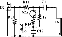
Figure 13 is the embodiment of the Drive and Control Circuit of second switch element Q2.
Following brief description reference numeral.
1,3-delay circuit; 2,4-ON time control circuit; 5-circuit overcurrent protection; 6-overcurrent protection input forming circuit; Q1-first switch element; Q2-second switch element; T-transformer; L-inductance.
Embodiment
Fig. 1 is the circuit diagram of the switching power unit of example 1 of the present invention.
Elementary at transformer T, on its primary coil T1 and the series circuit of inductance L, the connected first switching circuit S1 and input power supply Vin, and the series circuit of second switch circuit S2 and capacitor C is connected in parallel on the series circuit of described primary coil T1 and inductance L.In addition, the rectifier smoothing circuit that comprises rectifier cell Ds is connected on the secondary coil T2 of transformer T.
The first switching circuit S1 is made of the first switch element Q1, the first diode D1, the first capacitor C1 of parallel connection.Second switch circuit S2 is made of second switch element Q2, the second diode D2, the second capacitor C2 of parallel connection.
On transformer T, be provided with the first drive coil T3 and the second drive coil T4, connect first ON-OFF control circuit between the control end of the first drive coil T3 and the first switch element Q1, be provided with the second switch control circuit between the control end of the second drive coil T4 and second switch element Q2.This first and second ON-OFF control circuit is controlled this switch element, alternately conducting/disconnection during making that it clips that first, second switch element Q1, Q2 disconnect, during the first switch element Q1 conducting, in primary coil T1 and inductance L, put aside energy, off period in the first switch element Q1 releases energy from secondary coil T2, makes the first switch element Q1 and second switch element Q2 self-oscillation.
Described first ON-OFF control circuit is made of delay circuit 1 and ON time control circuit 2.
Delay circuit 1 is made of the series circuit of resistance R 3 and capacitor C 3, and being applied on the control end of the first switch element Q1 behind the voltage delay that takes place among the first drive coil T3.Be set to since the first drive coil T3, to take place voltage the time of delay that is provided with in this delay circuit 1 and drop to time of no-voltage, perhaps drop near the time the no-voltage to the charging charge that is added to the capacitor C1 on the first switch element Q1 two ends that are in off-state.Thus, near the first switch element Q1 conducting later on voltage that is added to its two ends drops to no-voltage or no-voltage.
Described ON time control circuit 2 has: to be connected first switch element between reference potential (negative pole) end of the control end of the first switch element Q1 and input power supply Vin be transistor Tr 1, be connected the series circuit of the phototransistor of resistance R 4 between the control end of the time constant circuit, the control end that is connected this transistor Tr 1 and the first switch element Q1 that are made of resistance R 2 and capacitor C4 on the control end of transistor Tr 1 and optical coupler PC.The time constant circuit of resistance R 2 and capacitor C4 is connected on the first drive coil T3, and behind the generation voltage, after preset time, transistor Tr 1 conducting disconnects the first switch element Q1 in the first drive coil T3.In addition, the series circuit of described phototransistor and resistance R 4 is according to the signal from output voltage detecting circuit described later, and the ON time of oxide-semiconductor control transistors Tr1 is to realize the stabilisation of output voltage V o.
Described second switch control circuit is made of delay circuit 3 and ON time control circuit 4.
Delay circuit 3 is applied on the control end of second switch element Q2 after with the voltage delay that produces among the second drive coil T4.Same with described delay circuit 1, be set to since the second drive coil T4, to produce voltage the time of delay of this delay circuit 3 and drop near no-voltage or the no-voltage time to the voltage that is added to second switch element Q2 two ends.Thus, second switch element Q2 also carries out zero voltage switch.In addition, ON time control circuit 4 has: be connected second switch unit on the second switch element Q2 control end and be transistor Tr 2 and be connected the time constant circuit that is made of resistance R 12 and capacitor C12 on these transistor Tr 2 control ends.The time constant circuit of resistance R 12 and capacitor C12 after preset time, makes transistor Tr 2 conductings after the voltage of the second drive coil T4 produces, second switch element Q2 is disconnected.In addition, as mentioned above, the set time constant of time constant circuit that is made of resistance R 12 and capacitor C12 series connection will satisfy this condition: in the second drive coil T4, produce after voltage, the second switch element Q2 conducting discharge end to secondary coil T2 energy before, cut off the series circuit current that flows to second switch element Q2 and inductance L forcibly, second switch element Q2 is disconnected.
On the described first switch element Q1, connected the circuit overcurrent protection 5 that comprises the resistance R that detects the electric current I d1 size that flows to this switch element Q1.Circuit overcurrent protection 5 comprises: the resistance R, its base stage that detect described electric current I d1 size are by the diode D3 between the control end of resistance R 5 and the transistor Tr 3 of resistance R 6 input resistance R both end voltage, the collector terminal that is connected transistor Tr 3 and the first switch element Q1.6 voltage dividing potential drops of this circuit overcurrent protection 5 usefulness resistance R5 and resistance R corresponding to the size of the electric current I d1 that flows to resistance R; offer between the base stage-collector electrode of transistor Tr 3; when this voltage surpassed threshold value Vbe (about 0.6V), transistor Tr 3 conductings disconnected the first switch element Q1.Thus, flowing to primary coil T1 and the first switch element Q1 current peak is restricted to set-point, can prevent that the transformer that overcurrent causes is saturated.
And when overcurrent, also the second ON time control circuit of the time constant circuit that constitutes by resistance R 2 and the capacitor C4 that comprises by ON time control circuit 2 carries out overcurrent protection.As described later; pattern from output voltage stabilizationization; if increasing, flow to the current peak of the electric current I d1 of the first switch element Q1, the output current Io from secondary coil T2 increases to more than the certain value; then circuit overcurrent protection 5 work; current peak is suppressed; but,, remain power output certain and the falling characteristic pattern reduction output voltage with regard to becoming if further increase output current Io.At this moment, describe in detail as the back, the described time constant circuit of ON time control circuit 2 shifts to an earlier date the conducting timing of transistor Tr 1, thus, controls, and the maximum ON time of the first switch element Q1 is shortened.Therefore, when overcurrent, the first, limited current peak by circuit overcurrent protection 5, the second, stipulated the maximum ON time of the first switch element Q1 by ON time control circuit 2.Thus, not only prevent the saturated of transformer, can also suppress the increase of secondary output current, or reduced short circuit current.In this example, described circuit overcurrent protection 5 is second ON time limiting units of the present invention, and ON time control circuit 2 constitutes the first ON time limiting unit of the present invention.
Overcurrent protection input correction circuit 6 is connected on the circuit overcurrent protection 5.In the present invention, this overcurrent protection input correction circuit 6 also is regarded as the part of circuit overcurrent protection.
Overcurrent protection input correction circuit 6 is connected between the base terminal of transistor Tr 3 of the first drive coil T3 and circuit overcurrent protection 5, is made of the series circuit of diode D4, Zener diode D5 and resistance R 7.This circuit is the output current when being used to revise circuit overcurrent protection 5 actions when input voltage changes.That is, when input voltage was high, the voltage that produces among the first drive coil T3 also raise, so by the circuit with this correction circuit 6, make the base terminal of current direction transistor Tr 3, reduced the operating point of circuit overcurrent protection.By like this,, can make the operating point of circuit overcurrent protection almost certain for the change of input voltage.
The output voltage detecting circuit 7 that detects output voltage V o is arranged on output one side of the secondary coil T2 of transformer T.
This output voltage detecting circuit 7 comprises: the divider resistance R20 and the R21 of output voltage V o dividing potential drop; The photodiode of the optical coupler PC that the tie point of this two resistance (datum mark) is connected to shunt regulator IC1 on the input of its reference voltage Vr, connect with this shunt regulator IC1.Shunt regulator IC1 reference voltage Vr with compare based on the branch pressure voltage Va of divider resistance R20, R21, come electric current between control cathode-anode according to its difference.Optical coupler PC changes a little less than the variation of this electric current is transformed to light intensity.If promptly output voltage V o raises, then the impedance between the collector electrode-emitter of the phototransistor of ON time control circuit 2 diminishes, thus, the charging interval of capacitor C4 in the conduction period of the first switch element Q1 in advance, the first earlier conducting of switch element Q1, the disconnection timing advance of transistor Tr, ON time shortens.If the ON time of the first switch element Q1 shortens, output current just reduces, and output voltage V o descends.Be lower than given voltage (voltage is set) if output voltage V o drops to, then by with above-mentioned opposite action, power output increases, output voltage rises.So just carried out the Stabilization Control of output voltage.
Below, the action of described switching power unit is described.
Fig. 2 is the oscillogram of circuit shown in Figure 1.Below, see figures.1.and.2, describe the action of this circuit in detail.
In Fig. 2, S1, S2 are the signals of conducting/disconnection of the expression first switch element Q1, second switch element Q2, Vds1, Vds2, Vs are respectively the both end voltage waveforms of capacitor C1, C2, Cs, and Id1, Id2, Is are respectively the current waveforms of switching circuit S1, S2, rectifier cell Ds.
Switch motion under the best stabilized state of this circuit can be divided into four operate conditions of time t1~t5 in a switch periods T.Below, the action of each state is described.
(state 1) t1~t2
The first switch element Q1 conducting increases by making the primary current straight line on the primary coil T1 that input voltage is applied to transformer T.At this moment, in transformer T, put aside magnetization energy.In addition, at this moment, filled electricity for capacitor C4 by optical coupler PC, if the voltage of this capacitor C4 arrives the threshold voltage (about 0.6V) of transistor Tr 1, this transistor Tr 1 disconnects at the moment t2 first switch element Q1 with regard to conducting, changes state 2 into.
(state 2) t2~t3
When the first switch element Q1 disconnects, the primary coil T1 of transformer T and inductance L and capacitor C1 and C2 resonance, capacitor C1 charging, capacitor C2 discharge.In addition, secondary, the secondary coil T2 of transformer T and capacitor Cs resonance, capacitor Cs discharge.The curve of the rising of voltage Vds1 and the sloping portion of Vds2 is based on the part of sine wave of the resonance of primary coil T1 and inductance L and capacitor C1 and capacitor C2.If the both end voltage Vds2 of capacitor C2 drops to no-voltage, diode D2 becomes state 3 with regard to conducting.
At this moment, secondary, capacitor Cs both end voltage Vs drops to no-voltage, rectifier cell Ds conducting, the action of vanishing voltage turn-on.The curve of the sloping portion of this both end voltage Vs is based on the part of sine wave of the resonance of capacitor Cs and secondary coil T2.
(state 3) t3~t4
Under the state of diode D2 conducting, by offering the control end of second switch element Q2, this second switch element Q2 conducting behind the voltage delay that produces among delay circuit 3, the second drive coil T4 that constitute by capacitor 11 and resistance R 11.Thus, second switch element Q2 carries out the zero voltage switch action.State 3 times, elementary, diode D2 and second switch element Q2 conducting, inductance L and capacitor C begin resonance, capacitor C discharge.
At this moment, secondary, rectifier cell Ds conducting, the magnetization energy of putting aside among the transformer T discharges from secondary coil T2, exports by rectifier smoothing circuit.Under this state, the electric current I s that flows to rectifier cell Ds is the shape that is similar to after having added the exciting current Im that straight line reduces on the Id2 (based on the resonance current of elementary inductance L and capacitor C), so become the waveform that rises and have sinusoidal waveform profile more sharp from zero current.
Elementary, because of the voltage that produces in the second drive coil T4, capacitor C12 is by resistance R 1 charging, and this charging voltage one arrives the threshold voltage (about 0.6V) of transistor Tr 2, this transistor Tr 2 is with regard to conducting, and force disconnect flows to the resonance current of second switch element Q2.And at this moment the size of the described resonance current of Qie Duaning is near peak value, and its timing is moment t4.The time constant of the time constant circuit that is made of the resistance R 12 and the capacitor C12 of ON time control circuit 4 is set to the time constant that second switch element Q2 is disconnected at described moment t4.
(state 4) t4~t5
When second switch element Q2 disconnected, resonance current was cut off rapidly, changed by this electric current rapidly, produced voltage in inductance L, the voltage reversal of the primary coil T1 of transformer T.Inductance L and capacitor C1 and C2 resonance, by the magnetization energy of inductance L, capacitor C1 discharge, capacitor C2 charging.During when the both end voltage Vds1 of capacitor C1 decline and at moment t5 vanishing voltage, diode D1 conducting, state 4 finishes.Under the state of diode D1 conducting, by the delay circuit 1 that is made of resistance R 3, capacitor C3, the voltage that produces in the first drive coil T3 is delayed, and then offers the control end of the first switch element Q1.Thus, the zero voltage switch action has been carried out in the first switch element Q1 conducting.
Secondary, switch element Q2 one conducting, rectifier cell Ds just disconnects, and the both end voltage Vs of capacitor Cs begins to rise from no-voltage, is clamped on the voltage of secondary coil voltage and output voltage sum.
In a switch periods, carry out above action, repeat this action later on.
(with the comparison of in the past circuit)
Fig. 3 is the movement oscillogram that the spy opens the switching power unit of describing in the flat 11-187664 communique in the past.
In switching power unit in the past, the moment t4 that second switch element Q2 disconnects is in resonance current Id2 drops near the zero current.And in this example, the moment t4 that disconnects second switch element Q2 is that resonance current Id2 is when being near the peak current value.Promptly, in switching power unit in the past, after the magnetization energy of putting aside in the conduction period of the first switch element Q1 has discharged, second switch element Q2 disconnects, and then rectifier cell Ds disconnects, and produces back voltage at these diode two ends, so voltage reversal of transformer T, produce positive polarity voltage in the first drive coil T3, thus, the first switch element Q1 carries out turn-on action.And in the switching power unit of this example, secondary, before having discharged the magnetization energy that first switch element Q1 conduction period put aside, second switch element Q2 disconnects, thus, the voltage first switch element Q1 conducting by in the first drive coil T3, producing.Then,, produce back voltage, disconnect at the two ends of secondary rectifier cell Ds by the first switch element Q1 conducting.
As seen, in switching power unit in the past, secondary rectifier cell Ds disconnects the trigger point that becomes the first switch element Q1 conducting after having discharged magnetization energy, and in the switching power unit of this example, make second switch element Q2 disconnect becoming by ON time control circuit 4 when discharging magnetization energy and connect the trigger point of seeing the conducting first switch element Q1.And in the switching power unit of example of the present invention, will satisfy this condition when being provided with the time constant of ON time control circuit 4: second switch element Q2 disconnects when discharging described magnetization energy.Therefore, the basic difference of the switching power unit of switching power unit in the past and this example is in the ON time control circuit 4 varying in size of the time constant that is provided with.
Fig. 4 shows conducting/disconnection sequential of switch element Q1 and Q2, rectifier cell Ds, (A) expression device in the past of this figure, and (B) of this figure represents the device of this example.
As shown in the figure, in device in the past, in rectifier cell Ds, produce back voltage, disconnect and to become transformer generation voltage reversal, the trigger point of the first switch element Q1 conducting, and in the device of this example, make second liter of trigger point of closing element Q2 disconnection becoming transformer generation voltage reversal itself, the first switch element Q1 conducting by ON time control circuit 4.As shown in Figure 4, in the device of in the past device and this example, the conducting of each switch element Q1, Q2/disconnection pattern difference.
(action of output voltage stabilizationization)
About the action of the stabilisation of output voltage V o, the same with in the past device.
In regular event, voltage Va that obtains after with output voltage V o dividing potential drop with resistance R20 and resistance R 21 and the reference voltage Vr of shunt regulator IC1 are made comparisons.Under this state, when rising to, output voltage V o is higher than when voltage is set, be higher than reference voltage Vr by making branch pressure voltage Va, the cathode potential of shunt regulator IC1 descends, the photodiode conducting of optical coupler PC.Thus, the impedance that is arranged between the collector electrode-emitter of the phototransistor on the ON time control circuit 2 diminishes.Like this, capacitor C4 charging interval conduction period of the first switch element Q1 shifts to an earlier date, and the conducting of transistor Tr 1 shifts to an earlier date constantly.Therefore, the disconnection of the first switch element Q1 also shifts to an earlier date constantly.Thus, the ON time of the first switch element Q1 shortens, and power output reduces, and output voltage descends.
In addition, be lower than when voltage is set, become and described opposite action when output voltage V o drops to.Promptly become big by the impedance between the collector electrode-emitter of phototransistor, transistor Tr 12 conductings are postponed constantly, and the ON time of the first switch element Q1 is elongated, and power output increases, and output voltage rises.
According to above action,, voltage stablized output voltage V o with being set.At this moment output voltage V o is represented by following formula.
Vo=Vr×(R20+R21)/R21
(action of circuit overcurrent protection)
During overcurrent and the action of circuit overcurrent protection 5 when starting and overcurrent protection input correction circuit 6 as described below.
When power output increases, flows to the current peak increase of primary coil T1, saturated in order to prevent transformer T, circuit overcurrent protection 5 work.In Fig. 1, electric current one flows to resistance R, and this resistance R both end voltage just by resistance R 5 and resistance R 6 dividing potential drops, is provided between the base-emitter of transistor Tr 3.At this moment, when the emitter-to-base voltage of the electric current increase of flowing through resistance R, this resistance R both end voltage increase, transistor Tr 3 surpasses threshold value Vbe (about 0.6V), transistor Tr 3 conductings, the first drive coil T3 disconnects.Thus, limited the current peak that flows to primary coil T1, prevented that transformer T is saturated.
When current peak begins to be suppressed, when output current further increases, output voltage is descended, power output P
0Remain on peak power output.And when output current reached maximum output current, this was then controlled by ON time control circuit 2, and the maximum ON time of switch element Q1 is shortened.The capacitor C4 of ON time control circuit 2 in primary coil T1 and inductance L, put aside energy during in, generation is recharged with the voltage of the first drive coil T3 of the proportional voltage of primary coil T1 voltage, discharge from secondary coil T2 described energy during, then discharge by producing with the back voltage of the first drive coil T3 of the proportional back voltage of voltage of this secondary coil T2.By repeating this charging and discharge, the charging charge of capacitor C4 can not increase under stable state., when output voltage V o descends, at a time, will discharge fully, cause the charging charge of capacitor C4 to increase by the back voltage that produces among the first drive coil T3 charging charge with capacitor C4.Thus, the ON time of transistor Tr 1 shifts to an earlier date, the result, and the maximum ON time of the first switch element Q1 shortens.This maximum ON time descends along with output voltage V o and shortens.By this action, output current can not be increased to more than the maximum output current, becomes the pattern that output current and output voltage all descend.In addition, if this pattern is further made progress, then this just can't lean on the voltage that produces among the first drive coil T3 to make the first switch element Q1 conducting, becomes re-lighting that has limited ON time and the oscillation mode that stops, and power output descends significantly.
Fig. 5 has represented when described overcurrent, electric current I d1 when ON time control circuit 2 is started working for the maximum ON time that limits the first switch element Q1 and the variation of exciting current Im.The current peak Idp that flows to primary coil T1 is limited by circuit overcurrent protection 5, and by the control of ON time control circuit 2, the ON time of the first switch element Q1 shortens gradually, reaches starting failure of oscillations pattern at last.
Fig. 6 has represented the circuit overcurrent protection performance plot under the maximum ON time limit movement of the current peak limit movement of circuit overcurrent protection 5 and ON time control circuit 2.In Fig. 6; when output current Io reaches circuit overcurrent protection action starting point A; as shown in Figure 5, by the action of circuit overcurrent protection 5, with power output Po remain on peak power output and meanwhile reduce output voltage along with the increase of output current Io.When output current Io reached maximum output current place B point, then the action of ON time control circuit 2 became overridingly, and as shown in Figure 5, the maximum ON time of the first switch element Q1 (Ton max) shortens.Under this pattern, output current Io and output voltage V o together descend.The characteristic of representing with X has been represented the characteristic (falling characteristic) of the circuit overcurrent protection in the switching power unit in the past.In the circuit overcurrent protection characteristic of this example; because when output current Io reaches maximum output current, can after this electric current and voltage all be descended by control; so can control the increase of secondary output current Io, the short circuit current in the time of perhaps reducing short circuit.
It should be noted that, can represent to flow to the current peak Idp of primary coil T1 with following expression formula.
Idp=Vbe·(R5+R6)/R6/R。
Overcurrent protection input correction circuit 6 is revised the output current of circuit overcurrent protection 5 work when input voltage changes.Promptly when input voltage is high,,, make transistor Tr 3 conductings in advance so the circuit of this voltage by diode D4, Zener diode D5, resistance R 7 is applied on the base terminal of transistor Tr 3 because the voltage that produces among the first drive coil T3 raises.Promptly reduce the operating point of circuit overcurrent protection.Thus, for the change of input voltage, can make the operating point of circuit overcurrent protection almost certain.
As shown in Figure 2, second switch element Q2 is being to disconnect before near the exciting current Im vanishing near the peak value of resonance current Id2, and then, the first switch element Q1 conducting is so the waveform of electric current I d1 becomes trapezoidal wave.And under normal condition, the ON time of second switch element Q2 is controlled as almost certain, and the ON time of the first switch element Q1 also is controlled as almost certain, and thus, switching frequency also becomes almost certain.In addition, becoming trapezoidally by the waveform that makes electric current I d1, is that the device in the past of triangular wave is compared with this waveform, and under the situation that obtains same power output, current peak diminishes.Therefore, can make transformer T miniaturization, the miniaturization and and the high efficiency of energy implement device.
Fig. 7 is expression with respect to the figure of the variation of the electric current I d1 of the first switch element Q1 of load variations and exciting current Im.
Fig. 7 (A) has represented the variation switching frequency pattern that changes slightly with respect to load.Under this pattern, electric current I d1 becomes trapezoidal wave when heavy duty.In addition, the part energy of savings in inductance L and primary coil T1 produces the circulating current of regeneration in input one side when underload.
Fig. 7 (B) expression switching frequency one current waveform regularly.Current waveform when in addition, having reduced circulating current under Fig. 7 (C) expression underload.Among Fig. 7 (A), (B), (C), electric current I d1 is a trapezoidal waveform when heavy duty.And, these patterns the time constant value that can adjust delay circuit 1,3 and ON time control circuit 2,4 is set.
The waveform of electric current I d1 in Fig. 7 (D) expression conventional art.In the pattern of conventional art, even when heavy duty, the waveform of electric current I d1 or triangular wave.Fig. 8 has represented the relation of power output and switching frequency under each pattern of described Fig. 7.Fig. 8 (A)~(D) corresponds respectively to Fig. 7 (A)~(D).And Fig. 8 (C) has provided the ON time that shortens second switch element Q2 when the little underload of the output current shown in Fig. 7 (C) at the switching point place, the example that reduces circulating current.
In each pattern of this example shown in Fig. 7 (A)~(C), power output Po is when middle load and heavy duty, and switching frequency is almost certain.And in ring damping coil converter in the past and the self-excitation double-throw flyback converter in the past, when middle load and heavy duty, switching frequency all not necessarily, power output Po is big more to descend more.As shown in Figure 8, in the present embodiment, can suppress the decline of switching frequency, the result can make transformer T and level and smooth circuit miniaturization, can realize switching power unit miniaturization and on the whole.
Below, be illustrated with regard to other example of the present invention.
Fig. 9 has represented the brief configuration figure of the switching power unit of example 2 of the present invention.
In example 2, the primary coil T1 of transformer T, inductance L, the first switching circuit S1, input power supply Vin are cascaded, and the series circuit of second switch circuit S2 and capacitor C is in parallel with the described first switching circuit S1.
On this circuit structure, to compare with example 1, the voltage that is added on the capacitor C increases, still, because can reduce capacitance when putting aside the identical quantity of electric charge, so can realize the miniaturization and of capacitor C.
Figure 10 has represented the brief configuration figure of the switching power unit of example 3 of the present invention.
In this example, the primary coil T1 of transformer T, inductance L, capacitor C, the first switching circuit S1, input power supply Vin are cascaded.In addition, the series circuit of the primary coil T1 of second switch circuit S2 and transformer T, inductance L, capacitor C is in parallel.
The ON-OFF control circuit of this example elementary be the semibridge system structure.Therefore, be added to voltage on the first switching circuit S1 and the second switch circuit S2 and become and equate, than the decline of example 1 with input voltage.General withstand voltage low switch element is because conducting resistance is little, so can reduce conducting loss, the realization high efficiency that conducting resistance causes.In addition, also become approximately half,, realize the small-sized efficient rateization of transformer T so can reduce the coiling number because be added to voltage on the transformer T.In addition, be not the magnetization energy of ON time savings in transformer T at the first switching circuit S1, the electrostatic energy of savings in capacitor C also discharges at off period, so can reduce to flow to current peak, the effective current of transformer T and switching circuit, reduce the conducting loss, help high efficiency.
Figure 11 has represented the brief configuration figure of the switching power unit of example 4 of the present invention.
In this example, rectification level and smooth the voltage of commercial ac voltage as input voltage.In addition, use current transformer CT as output voltage detecting circuit.By using current transformer CT, can reduce the loss of output voltage detecting circuit.
Figure 12 has represented the embodiment of the Drive and Control Circuit of the first switch element Q1.
This embodiment is in Fig. 1, transistor Tr 1 and 1 displacement of transistor Tr of transistor Tr 3 usefulness.
Figure 13 is the embodiment of the Drive and Control Circuit of expression second switch element Q2.This embodiment responds output and signal and changes second switch element Q2 ON time.The phototransistor of optical coupler PC2 is for example connected with the photodiode of the optical coupler PC of Fig. 1, and as shown in the figure, the phototransistor of this optical coupler PC2 is connected with resistance R 14, is connected on the control end of transistor Tr 2.Thus, when underload, can shorten the ON time of second switch element Q2.By shortening the ON time of second switch element Q2 when the underload, can reduce circulating current, improve efficient.
And, in above example, can field-effect transistors constitute the first switch element Q1 and second switch element Q2.By making field-effect transistors, can use its parasitic capacitance as capacitor C1 or capacitor C2, can also use parasitic diode as diode D1 or diode D2.Thus, number of spare parts can be cut down, cost degradation, the miniaturization and of switching power unit can be realized.
In addition, can use leakage inductance that transformer T has as inductance L.Thus, number of spare parts can be cut down, cost degradation, the miniaturization and of switching power unit can be realized.
In addition,, can reduce the reverse recovery power consumption of rectifier cell Ds, realize high efficiency, and can realize low EMI noiseization by capacitive impedance Cs being connected the two ends of secondary commutation element Ds.
According to the present invention, particularly when middle load,, can reduce the current peak and the effective current that flow to the transformer T and first switching circuit by being to work under the continuous current mode of trapezoidal wave at the current waveform that flows to the first switch element Q1.Thus, can reduce the copper loss of transformer, the conducting loss of the first switch element Q1, can realize the miniaturization and of switching power unit, can realize high efficiency.
In addition, because with self-oscillation mode forming circuit, thus do not need drive circuits such as oscillator and " totem " circuit, thus can realize miniaturization and, cost degradation that the reduction because of number of spare parts brings.
In addition, because can drive the high-end second switch element Q2 different with second drive coil with the earth level of the first switch element Q1, so do not need pulse transformer and high withstand voltage drive IC etc., can reduce number of spare parts, realize high efficiency miniaturization and, the cost degradation of switching power unit.
In addition, in the present invention, because have the circuit overcurrent protection of the peak value of the electric current that detects and suppress to flow through the first switch element Q1, so when overcurrent and during starting, can prevent that the transformer T that the peak current value increase causes is saturated, switch element destroys.
In addition,, can make the ON time of second switch element Q2 almost certain, thus, can also be controlled to be the ON time of the first switch element Q1 almost necessarily, make switching frequency almost certain by the second ON time control circuit.So, can suppress switching frequency and descend, make transformer and level and smooth circuit miniaturization, can realize the miniaturization and of switching power unit.
In addition, in the present invention,, have such two the ON time limiting units independently of the first ON time limiting unit and the second ON time limiting unit as circuit overcurrent protection.Therefore, when overcurrent,,, control, the maximum ON time of the first switch element Q1 is shortened by the first ON time limiting unit if overcurrent condition further makes progress with the second ON time limiting unit peak limiting current value.Thus, the increase of secondary output current can be suppressed, short circuit current can be reduced.
Claims (18)
1. a switching power unit has input power supply, inductance L, capacitor C, first switching circuit and second switch circuit with the related connection of the primary coil of transformer T;
Has the rectifier cell Ds that links to each other with the secondary coil of described transformer T;
Parallel circuits by the first switch element Q1, the first diode D1 and the first capacitor C1 constitutes first switching circuit;
Parallel circuits by second switch element Q2, the second diode D2 and the second capacitor C2 constitutes the second switch circuit;
Be provided with between the control end that is connected last first drive coil that is provided with of described transformer T and the first switch element Q1, and between second drive coil that go up to be provided with of described transformer T and the second switch element Q2 and clip this first and second switch element Q1, Q2 all disconnect during make it the ON-OFF control circuit of alternate conduction/disconnection, in described primary coil and inductance L, put aside energy in first switch element Q1 conduction period, release energy from described secondary coil at the first switch element Q1 off period, thereby make the first switch element Q1 and second switch element Q2 self-oscillation;
It is characterized in that: described inductance L and described capacitor C are formed in the resonant circuit of described first switch element Q1 off period resonance;
Described ON-OFF control circuit has the first ON time control circuit and the second ON time control circuit, the former time constant setting satisfies condition and is: disconnect through making this first switch element Q1 after preset time in the described first switch element Q1 conducting, the latter's time constant setting satisfies condition and is: this second switch element Q2 is disconnected, thereby cutting off the resonance current of the series circuit that flows to this second switch element Q2 and described inductance L;
Under continuous current mode, work.
2. switching power unit according to claim 1, it is characterized in that: on the series circuit of the primary coil of described transformer T and described inductance L, connected described first switching circuit and described input power supply, and the series circuit of described second switch circuit and described capacitor C is connected in parallel on the series circuit of the primary coil of described transformer T and described inductance L.
3. switching power unit according to claim 1, it is characterized in that: the primary coil of described transformer T, described inductance L, described first switching circuit and described input power supply are cascaded, and the series circuit of described second switch circuit and described capacitor C is in parallel with described first switching circuit.
4. switching power unit according to claim 1, it is characterized in that: the primary coil of described transformer T, described inductance L, described capacitor C, described first switching circuit and described input power supply are cascaded, and described second switch circuit is connected in parallel on the series circuit of the primary coil of described transformer T, described inductance L and described capacitor C.
5. switching power unit according to claim 1; it is characterized in that: be provided with circuit overcurrent protection; this circuit has the current detecting unit that is connected on the described first switch element Q1, and reaches this first switch element ON time of threshold time limit system when the value of described first switch element of inflow that detects with this current detecting unit.
6. switching power unit according to claim 5; it is characterized in that: described circuit overcurrent protection has the 3rd switch element that described first switch element is disconnected; the 3rd switch element is connected on the control end of described first switch element; described the 3rd switch element conducting when the peak current value that flows to described current detecting unit reaches described threshold value disconnects described first switch element.
7. switching power unit according to claim 1, it is characterized in that: described ON-OFF control circuit have between the control end that is connected described first drive coil and the described first switch element Q1 and the control end of described second drive coil and described second switch element Q2 between the delay circuit that constitutes of the series circuit by resistance or resistance and capacitor, after being produced, the voltage of the described first switch element Q1 conducting is delayed, or the voltage that makes the described first switch element Q1 conducting in described first drive coil is delayed after producing, and this first switch element Q1 or second switch element Q2 just are switched on then.
8. switching power unit according to claim 7, it is characterized in that: described delay circuit is provided with time of delay, makes the voltage at the two ends that are added to described first switch element Q1 or described second switch element Q2 drop to no-voltage or near the back conducting of no-voltage.
9. switching power unit according to claim 1, it is characterized in that: the described first ON time control circuit has first switch element that the described first switch element Q1 is disconnected, the described first ON time control circuit makes the voltage of the described first switch element Q1 conducting produce through after preset time from described first drive coil, make this first switch element conducting, to allow the described first switch element Q1 disconnect.
10. switching power unit according to claim 1, it is characterized in that: the described second ON time control circuit has the second switch unit that described second switch element Q2 is disconnected, the described second ON time control circuit makes the voltage of described second switch element Q2 conducting produce the back before described secondary coil energy discharges end from described second drive coil, this second switch cell conduction, to allow described second switch element Q2 disconnect, cut off the electric current of the series circuit that flows to this second switch element Q2 and described inductance L.
11. switching power unit according to claim 1, it is characterized in that: each value setting of described inductance L and described capacitor C is satisfied this condition: thus when disconnecting described second switch element Q2 cut-out by described ON-OFF control circuit and flow to the electric current of described inductance L, the resonance current that flows to this inductance L and capacitor C is near peak current.
12. switching power unit according to claim 9 is characterized in that: the described first ON time control circuit has the response signal corresponding with output voltage and changes the circuit that the described first switch element Q1 becomes the time of disconnection.
13. switching power unit according to claim 6; it is characterized in that: described the 3rd switch element of described circuit overcurrent protection is made of transistor; this transistor is connected on the control end of the first switch element Q1; the voltage that produces in the described current detecting unit offers described transistorized control end by resistance; when the electric current that flows to the described first switch element Q1 reaches set-point; described transistorized control end voltage reaches threshold value; this transistor turns; the described first switch element Q1 is disconnected, and restriction flows to the peak current value of this first switch element Q1.
14. switching power unit according to claim 13; it is characterized in that: described circuit overcurrent protection by resistance and diode, is input to the voltage that produces on the described transistorized control end in described first switch element Q1 conduction period first drive coil.
15. switching power unit according to claim 13 is characterized in that described circuit overcurrent protection has: the second ON time limiting unit of stipulating the first ON time limiting unit of the maximum ON time of the described first switch element Q1 and disconnect the described first switch element Q1 when the electric current that flows to the described first switch element Q1 reaching set-point is two ON time limiting units independently so.
16. switching power unit according to claim 1 is characterized in that: described first switch element Q1 or described second switch element Q2 are made of field-effect transistor.
17. switching power unit according to claim 1 is characterized in that: the leakage inductance that has by described transformer T has constituted described inductance L.
18. switching power unit according to claim 1 is characterized in that: the two ends at described rectifier cell Ds have connected capacitive impedance.
Applications Claiming Priority (2)
| Application Number | Priority Date | Filing Date | Title |
|---|---|---|---|
| JP2001273915 | 2001-09-10 | ||
| JP2001273915A JP3707409B2 (en) | 2001-09-10 | 2001-09-10 | Switching power supply |
Publications (2)
| Publication Number | Publication Date |
|---|---|
| CN1405959A true CN1405959A (en) | 2003-03-26 |
| CN1241317C CN1241317C (en) | 2006-02-08 |
Family
ID=19099056
Family Applications (1)
| Application Number | Title | Priority Date | Filing Date |
|---|---|---|---|
| CNB021416826A Expired - Lifetime CN1241317C (en) | 2001-09-10 | 2002-09-10 | Switch power-supply device |
Country Status (5)
| Country | Link |
|---|---|
| US (1) | US6639811B2 (en) |
| JP (1) | JP3707409B2 (en) |
| KR (1) | KR100503770B1 (en) |
| CN (1) | CN1241317C (en) |
| GB (1) | GB2383203B (en) |
Cited By (7)
| Publication number | Priority date | Publication date | Assignee | Title |
|---|---|---|---|---|
| US7414864B2 (en) | 2004-02-03 | 2008-08-19 | Murata Manufacturing Co., Ltd. | Switching power supply apparatus |
| CN1742423B (en) * | 2004-02-03 | 2010-12-01 | 株式会社村田制作所 | switching power supply unit |
| CN102844974A (en) * | 2010-04-16 | 2012-12-26 | 株式会社村田制作所 | Switch control circuit and switching power supply device |
| CN102939704A (en) * | 2010-06-10 | 2013-02-20 | 株式会社村田制作所 | Switching control circuit and switching power supply apparatus |
| US8488348B2 (en) | 2007-06-20 | 2013-07-16 | Samsung Electronics Co., Ltd. | Switch mode power supply apparatus having active clamping circuit |
| CN103684371A (en) * | 2012-08-29 | 2014-03-26 | 西门子公司 | Output module and method for operating the output module |
| CN105934883A (en) * | 2014-01-27 | 2016-09-07 | 美国莱迪思半导体公司 | Apparatus, system and method for providing switching with a t-coil circuit |
Families Citing this family (37)
| Publication number | Priority date | Publication date | Assignee | Title |
|---|---|---|---|---|
| JP2003309982A (en) * | 2002-04-16 | 2003-10-31 | Mitsubishi Electric Corp | Power semiconductor devices |
| JP2006014559A (en) | 2004-06-29 | 2006-01-12 | Murata Mfg Co Ltd | Dc/dc converter |
| KR100586978B1 (en) * | 2004-08-10 | 2006-06-08 | 삼성전기주식회사 | LLC resonance DC / DC converter |
| US7272025B2 (en) * | 2005-01-18 | 2007-09-18 | Power Integrations, Inc. | Method and apparatus to control either a regulated or an unregulated output of a switching power supply |
| JP5042536B2 (en) * | 2006-06-16 | 2012-10-03 | ローム株式会社 | POWER SUPPLY DEVICE AND ELECTRIC DEVICE HAVING THE SAME |
| JP4775441B2 (en) * | 2006-06-30 | 2011-09-21 | パナソニック電工株式会社 | Switching power supply |
| TWI319650B (en) * | 2006-11-17 | 2010-01-11 | Quanta Comp Inc | Power supply system |
| KR101052426B1 (en) * | 2007-01-19 | 2011-07-27 | 신덴겐코교 가부시키가이샤 | Switching power supply |
| JP5034568B2 (en) | 2007-03-09 | 2012-09-26 | 富士電機株式会社 | Switching power supply |
| TW200910750A (en) * | 2007-08-17 | 2009-03-01 | Murata Manufacturing Co | Switching power supply device |
| CN101471605B (en) * | 2007-12-29 | 2011-12-07 | 群康科技(深圳)有限公司 | Power supply circuit |
| JP5117980B2 (en) * | 2008-10-02 | 2013-01-16 | パナソニック株式会社 | Energy transfer device and semiconductor device for energy transfer control |
| US8284572B2 (en) * | 2008-11-20 | 2012-10-09 | Leadtrend Technology Corp. | Current control method and apparatus |
| CN101834063B (en) * | 2009-03-11 | 2012-05-30 | 王京申 | Pulse drive transformer assembly for self-excited switching power supply converter |
| JP5430186B2 (en) * | 2009-03-13 | 2014-02-26 | キヤノン株式会社 | Power supply device and control circuit |
| CN101964589A (en) * | 2009-07-22 | 2011-02-02 | Bcd半导体制造有限公司 | Method and device for controlling output current of convertor |
| TW201107952A (en) * | 2009-08-25 | 2011-03-01 | Elitegroup Computer Systems Co Ltd | Power-supply expansion system and its method thereof |
| TWI396375B (en) * | 2009-09-18 | 2013-05-11 | Leadtrend Tech Corp | Switching power supply and related control method |
| WO2011079250A1 (en) * | 2009-12-23 | 2011-06-30 | University Of New Hampshire | Fully resonant power supply |
| CN102763315B (en) * | 2010-02-23 | 2015-01-21 | 株式会社村田制作所 | Switching power supply unit |
| WO2011111483A1 (en) * | 2010-03-09 | 2011-09-15 | 株式会社村田製作所 | Switching power supply device |
| TWI392204B (en) * | 2010-07-06 | 2013-04-01 | Power Forest Technology Corp | Power conversion apparatus and over current protection method thereof |
| JP5549659B2 (en) * | 2011-10-28 | 2014-07-16 | 株式会社村田製作所 | Switching power supply |
| DE102011120805A1 (en) * | 2011-12-10 | 2013-06-13 | Minebea Co., Ltd. | down converter |
| CN104010406B (en) * | 2013-02-27 | 2016-12-28 | 台达电子工业股份有限公司 | Led driver |
| US9077254B2 (en) * | 2013-07-12 | 2015-07-07 | Solantro Semiconductor Corp. | Switching mode power supply using pulse mode active clamping |
| JP6403042B2 (en) * | 2014-02-28 | 2018-10-10 | パナソニックIpマネジメント株式会社 | Power supply apparatus and lighting apparatus using the same |
| JP6238300B2 (en) * | 2014-09-05 | 2017-11-29 | 新電元工業株式会社 | Switching power supply control method and control device |
| JP6372607B2 (en) * | 2015-02-17 | 2018-08-15 | 株式会社村田製作所 | DC-DC converter |
| US20180205311A1 (en) | 2017-01-17 | 2018-07-19 | Apple Inc. | Control of Series-Parallel Mode (SPM) Clamped Flyback Converter |
| US9774270B2 (en) | 2015-06-15 | 2017-09-26 | Apple Inc. | Systems and methods of operation for power converters having series-parallel mode active clamps |
| WO2017192058A1 (en) * | 2016-05-04 | 2017-11-09 | Закрытое Акционерное Общество "Драйв" | Method for generating a high pulse voltage in an inductive load |
| US10361638B2 (en) * | 2016-05-04 | 2019-07-23 | Drive Cjsc | Apparatus for generating high pulse voltage |
| JP2019092288A (en) * | 2017-11-14 | 2019-06-13 | キヤノン株式会社 | Power supply device and image forming device |
| US10158296B1 (en) | 2018-04-18 | 2018-12-18 | Nxp B.V. | Method and system for saturation control in a flyback switched-mode power supply (SMPS) |
| DE102018116883A1 (en) | 2018-07-12 | 2020-01-16 | Infineon Technologies Austria Ag | Flyback converter control, flyback converter and method for operating the flyback converter |
| JP2023181091A (en) * | 2022-06-09 | 2023-12-21 | サンケン電気株式会社 | Active clamp flyback converter and control IC |
Family Cites Families (16)
| Publication number | Priority date | Publication date | Assignee | Title |
|---|---|---|---|---|
| JPS59148562A (en) * | 1983-02-08 | 1984-08-25 | Sanken Electric Co Ltd | Dc/dc converter |
| JP2773195B2 (en) * | 1988-04-05 | 1998-07-09 | 松下電器産業株式会社 | Switching power supply |
| JPH0681500B2 (en) * | 1988-12-05 | 1994-10-12 | 富士通電装株式会社 | Switching circuit |
| US5055747A (en) * | 1990-07-20 | 1991-10-08 | Intent Patents A.G. | Self-regulating, no load protected electronic ballast system |
| JP2943269B2 (en) | 1990-07-25 | 1999-08-30 | 松下電器産業株式会社 | Switching power supply |
| JP3419797B2 (en) * | 1992-01-10 | 2003-06-23 | 松下電器産業株式会社 | Switching power supply |
| JPH0636392A (en) | 1992-07-17 | 1994-02-10 | Matsushita Electric Ind Co Ltd | Magnetic recording and reproducing device |
| JP2596142Y2 (en) * | 1992-10-05 | 1999-06-07 | ネミック・ラムダ株式会社 | Flyback type converter |
| JPH06169566A (en) * | 1992-11-30 | 1994-06-14 | Murata Mfg Co Ltd | Switching power supply device |
| US5570278A (en) | 1994-02-25 | 1996-10-29 | Astec International, Ltd. | Clamped continuous flyback power converter |
| JPH08168249A (en) * | 1994-10-11 | 1996-06-25 | Sony Corp | Current resonance type switching power supply circuit |
| JP3175663B2 (en) * | 1997-10-17 | 2001-06-11 | 株式会社村田製作所 | Self-oscillation type switching power supply |
| JP3201324B2 (en) * | 1997-12-22 | 2001-08-20 | 株式会社村田製作所 | Switching power supply |
| JP3475887B2 (en) * | 2000-01-11 | 2003-12-10 | 株式会社村田製作所 | Switching power supply |
| JP3475892B2 (en) * | 2000-02-25 | 2003-12-10 | 株式会社村田製作所 | Switching power supply |
| JP3675389B2 (en) * | 2001-03-26 | 2005-07-27 | 株式会社村田製作所 | Switching power supply device and electronic device using the same |
-
2001
- 2001-09-10 JP JP2001273915A patent/JP3707409B2/en not_active Expired - Fee Related
-
2002
- 2002-09-03 US US10/232,901 patent/US6639811B2/en not_active Expired - Lifetime
- 2002-09-10 CN CNB021416826A patent/CN1241317C/en not_active Expired - Lifetime
- 2002-09-10 GB GB0220965A patent/GB2383203B/en not_active Expired - Lifetime
- 2002-09-10 KR KR10-2002-0054521A patent/KR100503770B1/en not_active Expired - Lifetime
Cited By (12)
| Publication number | Priority date | Publication date | Assignee | Title |
|---|---|---|---|---|
| US7414864B2 (en) | 2004-02-03 | 2008-08-19 | Murata Manufacturing Co., Ltd. | Switching power supply apparatus |
| CN100463348C (en) * | 2004-02-03 | 2009-02-18 | 株式会社村田制作所 | Switching power supply equipment |
| CN1742423B (en) * | 2004-02-03 | 2010-12-01 | 株式会社村田制作所 | switching power supply unit |
| US8488348B2 (en) | 2007-06-20 | 2013-07-16 | Samsung Electronics Co., Ltd. | Switch mode power supply apparatus having active clamping circuit |
| CN102844974A (en) * | 2010-04-16 | 2012-12-26 | 株式会社村田制作所 | Switch control circuit and switching power supply device |
| CN102844974B (en) * | 2010-04-16 | 2015-09-16 | 株式会社村田制作所 | Switch control circuit and switching power supply device |
| US9142947B2 (en) | 2010-04-16 | 2015-09-22 | Murata Manufacturing Co., Ltd. | Switching control circuit and switching power supply apparatus |
| CN102939704A (en) * | 2010-06-10 | 2013-02-20 | 株式会社村田制作所 | Switching control circuit and switching power supply apparatus |
| CN102939704B (en) * | 2010-06-10 | 2015-08-12 | 株式会社村田制作所 | ON-OFF control circuit and switching power unit |
| CN103684371A (en) * | 2012-08-29 | 2014-03-26 | 西门子公司 | Output module and method for operating the output module |
| CN105934883A (en) * | 2014-01-27 | 2016-09-07 | 美国莱迪思半导体公司 | Apparatus, system and method for providing switching with a t-coil circuit |
| CN105934883B (en) * | 2014-01-27 | 2018-12-04 | 美国莱迪思半导体公司 | For providing the devices, systems, and methods of switching using T coil circuit |
Also Published As
| Publication number | Publication date |
|---|---|
| KR20030022727A (en) | 2003-03-17 |
| JP2003088117A (en) | 2003-03-20 |
| US6639811B2 (en) | 2003-10-28 |
| JP3707409B2 (en) | 2005-10-19 |
| GB2383203B (en) | 2004-05-05 |
| KR100503770B1 (en) | 2005-07-26 |
| US20030048645A1 (en) | 2003-03-13 |
| GB2383203A (en) | 2003-06-18 |
| GB0220965D0 (en) | 2002-10-23 |
| CN1241317C (en) | 2006-02-08 |
Similar Documents
| Publication | Publication Date | Title |
|---|---|---|
| CN1405959A (en) | Switch power-supply device | |
| CN1244976C (en) | Switching power supply unit | |
| CN1040272C (en) | Inverter device | |
| CN1238955C (en) | Switch power source apparatus | |
| CN1182648C (en) | switching power supply circuit | |
| CN1179477C (en) | piezoelectric inverter | |
| CN1249904C (en) | Switch power source | |
| CN1224161C (en) | Switching power supply device | |
| CN1360750A (en) | Switching power supply circuit | |
| CN1347190A (en) | Switch power supply with serial capacitances | |
| CN1885704A (en) | Switching power supply device | |
| CN1906839A (en) | Power factor improving circuit | |
| CN1125528C (en) | Switch power circuit | |
| CN1324141A (en) | Switching electric power supply device having active clamping circuir | |
| CN1378331A (en) | Switch power device and electronic device for using said switch power device | |
| CN1860671A (en) | Switching-mode power supply | |
| CN1171505C (en) | Magnetron drive power | |
| CN1238958C (en) | Switch power supply device | |
| CN1059295C (en) | Power supply apparatus | |
| CN1264271C (en) | Switch supply source | |
| CN1742424A (en) | Switching power supply equipment | |
| CN1812241A (en) | Switching power supply circuit | |
| CN1266821C (en) | Switch power-supply circuit | |
| CN1351409A (en) | DC-DC inverter and control thereof | |
| CN1140047C (en) | switching power supply circuit |
Legal Events
| Date | Code | Title | Description |
|---|---|---|---|
| C06 | Publication | ||
| PB01 | Publication | ||
| C10 | Entry into substantive examination | ||
| SE01 | Entry into force of request for substantive examination | ||
| C10 | Entry into substantive examination | ||
| SE01 | Entry into force of request for substantive examination | ||
| C14 | Grant of patent or utility model | ||
| GR01 | Patent grant | ||
| CX01 | Expiry of patent term | ||
| CX01 | Expiry of patent term |
Granted publication date: 20060208 |