CN1435721A - Picture pick-up device - Google Patents
Picture pick-up device Download PDFInfo
- Publication number
- CN1435721A CN1435721A CN03102099A CN03102099A CN1435721A CN 1435721 A CN1435721 A CN 1435721A CN 03102099 A CN03102099 A CN 03102099A CN 03102099 A CN03102099 A CN 03102099A CN 1435721 A CN1435721 A CN 1435721A
- Authority
- CN
- China
- Prior art keywords
- circuit
- mentioned
- photoelectric conversion
- conversion circuit
- image
- Prior art date
- Legal status (The legal status is an assumption and is not a legal conclusion. Google has not performed a legal analysis and makes no representation as to the accuracy of the status listed.)
- Granted
Links
Images



Classifications
-
- H—ELECTRICITY
- H04—ELECTRIC COMMUNICATION TECHNIQUE
- H04N—PICTORIAL COMMUNICATION, e.g. TELEVISION
- H04N23/00—Cameras or camera modules comprising electronic image sensors; Control thereof
- H04N23/60—Control of cameras or camera modules
- H04N23/67—Focus control based on electronic image sensor signals
-
- H—ELECTRICITY
- H04—ELECTRIC COMMUNICATION TECHNIQUE
- H04N—PICTORIAL COMMUNICATION, e.g. TELEVISION
- H04N23/00—Cameras or camera modules comprising electronic image sensors; Control thereof
- H04N23/60—Control of cameras or camera modules
- H04N23/65—Control of camera operation in relation to power supply
- H04N23/651—Control of camera operation in relation to power supply for reducing power consumption by affecting camera operations, e.g. sleep mode, hibernation mode or power off of selective parts of the camera
-
- H—ELECTRICITY
- H04—ELECTRIC COMMUNICATION TECHNIQUE
- H04N—PICTORIAL COMMUNICATION, e.g. TELEVISION
- H04N23/00—Cameras or camera modules comprising electronic image sensors; Control thereof
- H04N23/70—Circuitry for compensating brightness variation in the scene
- H04N23/71—Circuitry for evaluating the brightness variation
Landscapes
- Engineering & Computer Science (AREA)
- Multimedia (AREA)
- Signal Processing (AREA)
- Focusing (AREA)
- Studio Devices (AREA)
- Exposure Control For Cameras (AREA)
- Automatic Focus Adjustment (AREA)
- Solid State Image Pick-Up Elements (AREA)
- Transforming Light Signals Into Electric Signals (AREA)
Abstract
An image pickup apparatus includes a first photoelectric conversion circuit that has a photoelectric conversion area and is used for performing focus adjustment; a second photoelectric conversion circuit that has a photoelectric conversion area and is used for performing exposure amount adjustment; and a control circuit for controlling a power supply such that power is supplied to the first photoelectric conversion circuit and the second photoelectric conversion circuit independently, in which the first photoelectric conversion circuit and the second photoelectric conversion circuit are formed on a same semiconductor substrate.
Description
Technical field
The present invention relates to have the image-pickup device of light-to-current inversion function.
Background technology
Figure 11 is the multiple point distance measurement that uses in the Single-sens reflex camera that is illustrated in the in the past block scheme with an example of automatic focus sensor circuit.This automatic focus sensor is that the inventor herein waits at (Japan) image information medium technical report Vol.25 of association No28, PP.1~6, the sensor that Mar.2001 delivers.Among this figure, the 900th, semi-conductor chip (semiconductor substrate), the 901st, AF sensor circuit piece, the 902nd, analog circuit block, the 903rd, digital circuit block.
In order to carry out 7 range findings (center is for intersecting range finding), AF circuit block 901 is made of 8 line-array sensor circuit 1A (1B)~8A (8B).Analog circuit block 902 by the agc circuit 1~8 of the accumulated time that is used for controlling each line-array sensor circuit, amplify output and constitute from the signal amplification circuit 902A of the signal of AF sensor circuit piece 902, band-gap circuit (reference potential generative circuit) 902B that generates reference potential, the intermediate potential generative circuit 902C that is created on sensor circuit and mimic channel required voltage.
Digital circuit block 903 by be used to carry out with the input/output communication circuit (I/O) of communicating by letter of microcomputer, be used to generate the driving pulse of sensor timing generator circuit (T/G), be used to select the multi-path converter circuit (MPX) of various simulating signals to constitute.Because Single-sens reflex camera requires high-speed automatic focusing, so in the AF sensor, realize high speed motion by 8 line-array sensor circuit of driving arranged side by side and agc circuit.
But in above-mentioned automatic focus sensor in the past, the current drain when driving each circuit simultaneously and will cause moving increases.Do not constitute too much problem though in Single-sens reflex camera, can carry the battery of high current capacity, in the minicam of the battery that can only carry little current capacity, then have significantly the shorten problem of this class of the battery life of camera.
In addition, because the AE in the minicam is different with the TTL mode of Single-sens reflex camera with AF, be the AE and the AF of outer survey mode, so exist because of the doubly regional problem that makes unwanted AF circuit (it is outer that the point distance measurement of AF sensor is positioned at camera watch region) action of the change of employed imaging lens system.
Summary of the invention
The objective of the invention is to reduce power consumption.
In order to achieve the above object, the invention provides a kind of image-pickup device, comprising: have the light-to-current inversion zone, and for carrying out the 1st photoelectric conversion circuit that the focus adjustment is used; Have the light-to-current inversion zone, and for carrying out the 2nd photoelectric conversion circuit that the exposure adjustment is used; And control the control circuit that makes independently to above-mentioned the 1st photoelectric conversion circuit and the power supply of above-mentioned the 2nd photoelectric conversion circuit; Above-mentioned the 1st photoelectric conversion circuit and above-mentioned the 2nd photoelectric conversion circuit are formed on the same semiconductor substrate.
In addition, the invention provides a kind of image-pickup device, comprising: the 1st, the 2nd photoelectric conversion circuit that comprises the light-to-current inversion zone respectively; And according to the action of the Zoom lens that is used to amplify, dwindle the subject picture that will absorb, switch not to above-mentioned the 1st photoelectric conversion circuit power supply ground, to the pattern of the 2nd photoelectric conversion circuit power supply with simultaneously to the control circuit of the pattern of the above-mentioned the 1st and the 2nd photoelectric conversion circuit power supply.
In addition, the invention provides a kind of image-pickup device, comprising: the 1st, the 2nd photoelectric conversion circuit that comprises light-to-current inversion zone and log compression circuit respectively; With above-mentioned the 1st, the 2nd photoelectric conversion circuit be the center be arranged on the one side, have an a plurality of light-to-current inversions zone and read the 3rd, the 4th photoelectric conversion circuit of sensing circuit of the peak signal in above-mentioned a plurality of light-to-current inversions zone respectively; With above-mentioned the 1st, the 2nd photoelectric conversion circuit be the center be arranged on its other side, have an a plurality of light-to-current inversions zone and read the 5th, the 6th photoelectric conversion circuit of sensing circuit of the peak signal in above-mentioned a plurality of light-to-current inversions zone respectively; And control and make not to above-mentioned the 1st, 3,5 photoelectric conversion circuits power supply ground, to the control circuit of above-mentioned the 2nd, 4,6 photoelectric conversion circuits power supply; Above-mentioned the 1st~6 photoelectric conversion circuit is formed on the same semiconductor substrate.
In addition, the invention provides a kind of image-pickup device, comprising: the 1st photoelectric conversion circuit that comprises light-to-current inversion zone and log compression circuit respectively; With above-mentioned the 1st photoelectric conversion circuit be the center be arranged on the one side, have a plurality of light-to-current inversions zone and read the 2nd photoelectric conversion circuit of sensing circuit of the peak signal in above-mentioned a plurality of light-to-current inversions zone; And control the control circuit that makes independently to above-mentioned the 1st photoelectric conversion circuit and the power supply of above-mentioned the 2nd photoelectric conversion circuit; Above-mentioned the 1st, the 2nd photoelectric conversion circuit is formed on the same semiconductor substrate.
Description of drawings
Fig. 1 is the block scheme of formation of the 1st form of implementation of expression photometry ranging solid state image pick-up of the present invention;
Fig. 2 is the planar configuration of the 1st form of implementation of the present invention;
Fig. 3 is the circuit diagram of the AF sensor circuit of expression the 1st form of implementation;
Fig. 4 A~4D is the action of the AF sensor circuit of explanation the 1st form of implementation, the figure of non-action;
Fig. 5 is the circuit diagram of the AE sensor circuit of expression the 1st form of implementation;
Fig. 6 A~6C is the figure of the agc circuit of expression the 1st form of implementation;
Change when Fig. 7 A~7C is the shooting of explanation the 1st form of implementation is the figure of zone and the relation of AE circuit that moves and AF circuit doubly;
Fig. 8 is the block scheme of the formation of expression the 2nd form of implementation of the present invention;
Fig. 9 is the planar configuration of the 2nd form of implementation of the present invention;
Figure 10 is the block diagram of a form of implementation that the image-pickup device of photometry ranging solid state image pick-up of the present invention has been used in expression;
Figure 11 represents the figure of routine in the past multiple point distance measurement with the automatic focus sensor.
Embodiment
Below, at length form of implementation of the present invention is described with reference to drawing.
The 1st form of implementation
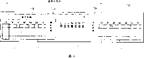
Fig. 1 is the block scheme of formation of the 1st form of implementation of expression photometry ranging solid state image pick-up of the present invention, the planar configuration of the solid camera head of Fig. 2 the 1st form of implementation.The photometry ranging solid state image pick-up of this form of implementation (is used to adjust the function of focus) and has also carried photometry function (being used to adjust the function of exposure) except distance measurement function.Among the figure, the 100th, semi-conductor chip (semiconductor substrate), the 101st, have the light-to-current inversion zone and be used to carry out the AF circuit block that focus is adjusted, the 103, the 104th, have the light-to-current inversion zone and be used to carry out the AE circuit block that exposure is adjusted, the 105th, analog circuit block, the 106th, digital circuit block.Each piece is integrated on the semi-conductor chip 100.
Show AE sensor light photodiode area 103 and AE circuit block 104 as a piece among Fig. 1, as shown in Figure 2, AE sensor light photodiode area 103 is configured in the central portion of semi-conductor chip 100, and AE circuit block 104 is configured in its next door.As shown in Figure 2, AE sensor light photodiode area 103 is divided into 16 zones, is made of with photodiode T with photodiode M1~M4,1 photometry of looking in the distance with photodiode W1~W4,4 standard photometries with photodiode S1~S7,4 wide-angle photometries the photometry of 7 points.
Here, as shown in Figure 1, AE circuit block 104 includes AE circuit S1~S7, AE circuit W1~W4, AE circuit M1~M4, AE circuit T, and they are the AE circuit of current/voltage log-transformation type.In addition, in these circuit, AE circuit S1~S7 corresponds respectively to the photodiode S1~S7 of the AE sensor light photodiode area 103 of Fig. 2, AE circuit W1~W4 corresponds respectively to photodiode W1~W4, AE circuit M1~M4 corresponds respectively to photodiode M1~M4, and AE circuit T is corresponding to photodiode T.In addition, AE circuit block 104 is also comprising Is (diode reverse electric current) compensating circuit 104a, signal amplification circuit 104b.
As shown in Figure 2, analog circuit block 105 is configured in the next door of AE sensor light photodiode area 103, is made of the agc circuit 1~7 of the accumulated time that is used to control each AF sensor circuit 102, band-gap circuit (reference potential generative circuit) 105a that generates reference potential, the intermediate potential generative circuit 105b that is used to generate intermediate potential, the signal amplification circuit 105c that is used to amplify from the output of AF line-array sensor.
As shown in Figure 2, digital circuit block 106 is configured in the next door of analog circuit block 105, by be used to carry out with the input/output communication circuit (I/O) of communicating by letter, AF circuit, the AE circuit of microcomputer (not diagram), be used to generate the driving pulse of agc circuit timing generator circuit (T/G), be used to select the multi-path converter circuit (MPX) of various simulating signals to constitute.As being described in detail later, each AF circuit, AE circuit, agc circuit are used to the control signal control action from the T/G circuit, non-action based on control of microcomputer.
Fig. 3 is the concrete circuit diagram of the AF sensor circuit 102 of Fig. 1.Among this figure, the 1st, carry out the PN junction photodiode of light-to-current inversion, the 2nd, the current potential of PN junction photodiode is reset to resetting of VRES use MOS transistor, the 3rd, be used to be amplified in the differential amplifier circuit of the electric charge that the PN junction photodiode produces, the 4th, be used to store the mos capacitance of the output voltage of differential amplifier circuit, the 5th, the storage switch MOS transistor, the 6th, be used to remain on the source follower circuit that the amplification of the electric charge of mos capacitance 4 is read.Here, feed back to differential amplifier circuit 3 by the output with source follower circuit 6, the bias deviation and the gain that can suppress output voltage reduce.
The 7th, clamping capacitance, the 8th, be used to import the MOS switch of clamping capacitance, constitute clamp circuit by 7 and 8.9~12nd, the switch MOS transistor, the 13rd, minimum value detects with differential amplifier (minimum value testing circuit), and the 14th, maximal value detects with differential amplifier (maximum value detecting circuit), and each differential amplifier constitutes voltage follower circuit.The 15th, the MOS switch is used in minimum value output, and the 16th, the MOS switch is used in maximal value output, and the 17th, or door, the 18, the 19th, constant current MOS transistor, the 20th, sweep circuit.In minimum value testing circuit 14, last level is used the source follower of NMOS, and in maximum value detecting circuit 15, last level is used the source follower of PMOS.The 21st, output is from the general output line of the AF signal of pixel.
In this circuit constitutes, by prime the noise clamp circuit of feedback-type is set, can removes reset noise that on photodiode, produces and the FPN that produces at sensor amplifier, maximum value detecting circuit, minimum value testing circuit at minimum value testing circuit 14 and maximum value detecting circuit 15.
In addition, by the voltage follower circuit of source follower form in the end is set the output stage individual element, when maximal value is exported, the constant current source of the output stage of each voltage follower is turn-offed, be connected to the output line that is connected in constant current source jointly, can obtain the minimum value of picture signal.In addition,, the constant current source of the output stage of each voltage follower is connected, can successively each voltage follower circuit be connected to output line, obtain the picture signal of serial by when the AF picture signal is exported.Utilize this action, but because dual-purpose maximum value detecting circuit and AF circuit for outputting image signal, so can realize the miniaturization of chip.
Fig. 4 A~4D represents the physical circuit figure of differential amplifier circuit of differential amplifier circuit, the minimum value testing circuit of differential amplifier circuit, source follower, the maximum value detecting circuit of the pixel portions of AF sensor circuit.Fig. 4 A is that differential amplifier circuit (differential amplifier circuit 3 of corresponding diagram 3), Fig. 4 B of pixel portions is that source follower 6, Fig. 4 C are that minimum value testing circuit 13, Fig. 4 D are the circuit of maximum value detecting circuit 14.
In addition, in Fig. 4 A~4D, provided the concrete circuit of each circuit.Which circuit has all used MOS transistor, in each circuit of Fig. 4 A~4D, and 41~46th, as the MOS transistor of constant current source.In this form of implementation, when the AF sensor circuit moves, the signal of action is applied on the grid by making this MOS transistor, can be used as constant current source and use.In addition, when the AF sensor circuit is failure to actuate, be applied on the grid, can turn-off bias current by the signal that this MOS transistor is ended.
Particularly, be added to the control signal on this grid, generated by the T/G circuit by the communication from microcomputer, control signal AFON1 shown in Figure 1~AFON7 and control signal AF2ON1~AF2ON7 are offered each self-corresponding AF circuit respectively.When making the AF circuit be operating state, such as the aforementioned, by making it to be applied on the grid of the MOS transistor 41~46 that constitutes constant current source the formation operating state in the control signal (intermediate level signal) of range of linearity action.
On the other hand, when making the AF circuit be non-action status, such as the aforementioned, (AFON1~7 o'clock are VDD level (power level signal) to control signal by will making it to end, AF2ON1~7 o'clock are the GND level signal) be applied on the grid of this MOS transistor 41~46, form non-action status.Here, control signal AF2ON1~AF2ON7 offers all circuit of Fig. 4 A~Fig. 4 D, and control signal AFON1~AFON7 then only offers the circuit of Fig. 4 C.
Fig. 5 represents the concrete example of log-transformation type AE circuit (comprising photodiode).It is corresponding to whole AE circuit of the AE circuit S1~S7 that comprises Fig. 1.500 is PN junction photodiodes among the figure, the 501st, and as the PN junction photodiode of the nonlinear element that is used to carry out log-compressed, the 502nd, the differential amplifier circuit that CMOS constitutes.In addition, in Fig. 5, show the concrete circuit of differential amplifier circuit 502 in the lump.Differential amplifier circuit 502 uses MOS transistor to constitute, and wherein 47,48 is PMOS transistor as constant current source.
By controlling this MOS transistor 47,48, can control the action of AE circuit, non-action.Particularly, as shown in Figure 1,, offered each self-corresponding AE circuit respectively from control signal AEON1~7, AEONT, AEONW, the AEONM of T/G circuit based on control of microcomputer.Control signal AEON1~7 correspond respectively to AE circuit S1~S7, and control signal AEONT is corresponding to AE circuit T, corresponding 4 the AE circuit W1~W4 of control signal AEONW, and control signal AEONM is corresponding to 4 AE circuit M1~M4.
Here, when the non-action of AE circuit, add the control signal of VDD level (power level) by the grid to MOS transistor 47,48, MOS transistor 47,48 is turn-offed, making the AE circuit by the bias current that turn-offs differential amplifier circuit 502 is non-action.In addition, when the action of AE circuit, be applied on its grid in the control signal (intermediate level signal) of range of linearity action, make the AE circuit become operating state by making MOS transistor 47,48.
Fig. 6 A represents the concrete circuit diagram of agc circuit.61 is voltage buffer circuits among the figure, the 62nd, and comparator circuit.As shown in Figure 1, the AF circuit 102 of agc circuit corresponding A F circuit block 101 is provided with, and agc circuit 1~7 corresponds respectively to the group setting of group~L7A and the L7B of horizontal line-array sensor L1A and L1B.
In each agc circuit, with voltage buffer circuit 61 impedance conversions from each behind the maximum value signal of self-corresponding AF circuit, carry out comparison with comparative voltage VBB with comparator circuit 62.And then, having surpassed the VBB place at maximum value signal from the AF circuit, the output of counter-rotating comparator circuit 62 finishes the accumulation of the photodiode in the AF circuit.
Fig. 6 B represents voltage buffer circuit 61, and Fig. 6 C represents the concrete circuit of comparator circuit 62.63, the 64th, the constant current MOS transistor of voltage buffer circuit 61, the 65th, the constant current MOS transistor of comparator circuit 62.Agc circuit passes through from the control signal AGCON1~AGCON7 control action of T/G circuit, non-action, and as shown in Figure 1, control signal AGCON1~AGCON7 corresponds respectively to agc circuit 1~7.
When the action of agc circuit,, make it to move as constant current source by constant current is added control signal from the intermediate level of T/G circuit with the grid of MOS transistor 63~65.On the other hand, when the non-action of agc circuit,, make it to become the electric current off state by constant current is added control signal from the VDD level (power level) of T/G circuit with the grid of MOS transistor 63~65.Can be corresponding to action, the non-action of the action of AF circuit, non-action control agc circuit, only make the agc circuit action of the AF circuit that correspondence moves, reduced current drain.
As above, utilize T/G circuit, can setover independently control AF circuit and AE circuit as control circuit.In addition, utilize T/G circuit, can also setover independently control AF circuit, AE circuit and agc circuit as control circuit.
Below, the change in the reality photography is doubly described with the AF sensor circuit that moves and the relation of AE sensor circuit in zone (wide-angle zone, standard area, the zone of looking in the distance).Table 1 expression becomes relation doubly regional and the AF sensor circuit that moves, and table 2 expression becomes relation doubly regional and the AE sensor circuit that moves.In addition, Fig. 7 A~Fig. 7 C represents to become doubly zone and the AF sensor circuit of action, the relation of AE sensor circuit.The sensor that the sensor that Fig. 7 A moves when representing the photography of wide-angle zone, the sensor that Fig. 7 B moves when representing the standard area photography, Fig. 7 C move when representing to look in the distance the zone photography.Here, zero circuit is the circuit of biasing ON in table 1, the table 2, and the photodiode area of representing with oblique line in Fig. 7 A~Fig. 7 C is the circuit of biasing ON.
Table 1
| Become doubly zone | The AF sensor | ||||||
| L1 | ?L2 | ?L3 | ?L4 | ?L5 | ?L6 | ?L7 | |
| (1) wide-angle | ○ | ?○ | ?○ | ?○ | ?○ | ?○ | ?○ |
| (2) standard | - | ?○ | ?○ | ?○ | ?○ | ?○ | ?- |
| (3) look in the distance | - | ?- | ?○ | ?○ | ?○ | ?- | ?- |
Table 2
| Become doubly zone | The AE sensor | |||||||||
| L1 | ?L2 | ?L3 | ?L4 | ?L5 | ?L6 | ?L7 | ?W1、W2、 ?W3、W4 | ?M1、M2、 ?M3、M4 | ??T | |
| (1) wide-angle | ○ | ?○ | ?○ | ?○ | ?○ | ?○ | ?○ | ???○ | ???○ | ??○ |
| (2) standard | - | ?○ | ?○ | ?○ | ?○ | ?○ | ?- | ???- | ???○ | ??○ |
| (3) look in the distance | - | ?- | ?○ | ?○ | ?○ | ?- | ?- | ???- | ???- | ??○ |
At first, when the photography of the wide-angle zone of Fig. 7 A, as shown in table 2 such, make all AE sensors (totally 16 of S1~S7, W1~W4, M1~M4, T) action carrying out photometry, as shown in table 1 such, all AF sensors (totally 7 of L1~L7) action is found range.Here, so-called L1~L7 refers to each group of horizontal line-array sensor L1A shown in Figure 1 and L1B~horizontal line-array sensor L7A and L7B.
When the standard area photography of Fig. 7 B, only make AF sensor (5) action carrying out photometry and the range finding of AE sensor (10 zones) and the L2~L6 of S1~S6, M1~M4, T.Other AF sensor and AE sensor are non-action status.Here, AF sensor L2~L6 refers to each group of horizontal line-array sensor L2A shown in Figure 1 and L2B~horizontal line-array sensor L6A and L6B.
When photograph in the zone of looking in the distance of Fig. 7 C, only make AF sensor (3) action carrying out photometry and the range finding of AE sensor (4 zones) and the L3~L5 of S3~S5, T.Other AF sensor and AE sensor are non-action status.In addition, similarly, AF sensor L3~L5 refers to each group of horizontal line-array sensor L3A shown in Figure 1 and L3B~horizontal line-array sensor L5A and L5B.In this some form of implementation below also is the same.
These become the doubly selection of the AF sensor in zone, as illustrating with Fig. 4, are undertaken by the control signal from the T/G circuit based on control of microcomputer.For example, in wide-angle when photography zone,, make all AF circuit operations and find range by all AF sensor circuits being added the signal (intermediate level signal) that makes the MOS transistor line movement that constitutes constant current source.
In addition, the selection of AE sensor also as illustrating with Fig. 5, is undertaken by the control signal from the T/G circuit.For example, such as the aforementioned when the photography of wide-angle zone, by all AE sensor circuits being added the signal (intermediate level signal) that makes the MOS transistor line movement that constitutes constant current source, make all AE circuit operations and carry out photometry.In addition, as illustrating with Fig. 6, be used to carry out from the control signal of T/G circuit the selection of agc circuit, can only make the agc circuit action of the AF circuit that correspondence moves and make the agc circuit of the AF circuit of corresponding non-action is non-action.When the photography of wide-angle zone, owing to all AF circuit all move, so make all agc circuit actions.
Like this, in this form of implementation, be operating state by in a plurality of AF circuit and AE circuit, only making the AF circuit and the AE circuit that need, to other AF circuit and AE circuit, turn-off constant current source and make it to become non-action status, can reduce current drain significantly.In addition, owing to can reduce current drain,, realize the automatic focus solid camera head of low power consumption so can be equipped on minicam.Here, the present invention not only is to use cmos sensor, also can be applied to for example situations such as CCD, BASIS, SIT, CMD, AMI.
The 2nd form of implementation
Fig. 8 is the figure of the 2nd form of implementation of expression photometry ranging solid state image pick-up of the present invention, and Fig. 9 is its planar configuration.In this form of implementation, the number of cutting apart of AE sensor is less than the 1st form of implementation.That is, the AE sensor is made of with AE circuit S1~S7 with AE circuit W and the photometry of 7 points whole photometry.W in the AE sensor light photodiode area 103 shown in Figure 9 is corresponding to the photodiode of whole photometry with AE circuit W, and S1~S7 corresponds respectively to the photodiode of a photometry with AE circuit S1~S7.Other formation is identical with the 1st form of implementation of Fig. 1.
The change of the imaging lens system in table 3 expression the 2nd form of implementation is zone (wide-angle zone, standard area, the zone of looking in the distance) and the AF sensor circuit that moves and the relation of AE sensor doubly.
Table 3
| The AF sensor | The AE sensor | ||||||||||||||
| L1 | ?L2 | ?L3 | ?L4 | ?L5 | ?L6 | ?L7 | ?S1 | ?S2 | ?S3 | ?S4 | ?S5 | ?S6 | ?S7 | ?W | |
| (1) wide-angle | ○ | ?○ | ?○ | ?○ | ?○ | ?○ | ?○ | ?○ | ?○ | ?○ | ?○ | ?○ | ?○ | ?○ | ?○ |
| (2) standard | - | ?○ | ?○ | ?○ | ?○ | ?○ | ?- | ?- | ?○ | ?○ | ?○ | ?○ | ?○ | ?- | ?○ |
| (3) look in the distance | - | ?- | ?○ | ?○ | ?○ | ?- | ?- | ?- | ?- | ?○ | ?○ | ?○ | ?- | ?- | ?○ |
At first, when the photography of wide-angle zone, make the action carrying out of all AE sensors (8 zones) and AF sensor (7) photometry and range finding.When standard area is photographed, only make AF sensor (5) action carrying out photometry and the range finding of AE sensor (6 zones) and the L2~L6 of S2~S6, W.When being visible the photography of territory, far field, only make AF sensor (3) action carrying out photometry and the range finding of AE sensor (4 zones) and the L3~L5 of S3~S5, W.With the 1st form of implementation of Fig. 1 similarly, the selection of AF sensor, the action of AE sensor, non-action is used to carry out from the control signal of T/G circuit.In addition, also with the 1st form of implementation similarly, carry out the selection action of agc circuit corresponding to the action of AF sensor circuit, non-action.
Like this, in this form of implementation, with the 1st form of implementation of Fig. 1 similarly, by in a plurality of AF circuit and AE circuit, only making the AF circuit and the AE circuit that need become operating state, AF circuit and AE circuit shutoff constant current source to other make it to become non-action status, can reduce current drain significantly.In addition, can simplify formation, can also further reduce power consumption by reducing the AE number of sensors.
The 3rd form of implementation
Below, the 3rd form of implementation of the present invention is described.The 3rd form of implementation is compared with the 1st form of implementation, and for the change doubly regional (wide-angle zone, standard area, the zone of looking in the distance) of photographic lens, the AF sensor that it moves is different with the AE sensor.The formation of device is the same with the 1st form of implementation.Table 4 provides the relation of the AF sensor that becomes times zone and move, and table 5 provides the relation of the AE sensor that becomes doubly regional and move.
Table 4
| Become doubly zone | The AF sensor | ||||||
| L1 | ?L2 | ?L3 | ?L4 | ?L5 | ?L6 | ?L7 | |
| (1) wide-angle | ○ | ?- | ?- | ?○ | ?- | ?- | ?○ |
| (2) standard | - | ?○ | ?- | ?○ | ?- | ?○ | ?- |
| (3) look in the distance | - | ?- | ?○ | ?○ | ?○ | ?- | ?- |
Table 5
| Become doubly zone | The AE sensor | |||||||||
| ??S1 | ??S2 | ??S3 | ??S4 | ?S5 | ??S6 | ??S7 | ??W1、W2 ??W3、W4 | ??M1、M2、 ??M3、M4 | ?T | |
| (1) wide-angle | ??○ | ??- | ??- | ??○ | ?- | ??- | ??○ | ????○ | ????○ | ?○ |
| (2) standard | ??- | ??○ | ??- | ??○ | ?- | ??○ | ??- | ????- | ????○ | ?○ |
| (3) look in the distance | ??- | ??- | ??○ | ??○ | ?○ | ??- | ??- | ????- | ????- | ?○ |
At first, when the photography of wide-angle zone, use the AF sensor of L1, L4, L7, use the AE sensor of S1, S4, S7 and W1~W4, M1~M4, T.When standard area is photographed, use the AF sensor of L2, L4, L6, use the AE sensor of S2, S4, S6, M1~M4, T.When being visible the photography of territory, far field, use the AF sensor of L3~L5, use the AE sensor of S3~S5, T.With the 1st form of implementation similarly, the selection of AF sensor, the action of AE sensor, non-action is used to carry out from the control signal of T/G circuit.In addition, also with the 1st form of implementation similarly, carry out the selection action of agc circuit corresponding to the action of AF sensor circuit, non-action.
In this form of implementation, it is characterized in that only using 3 pieces in the AF sensor circuit with 7 pieces, can always carry out 3 range findings thus.Thus, the range finding when having reduced wide-angle photography is counted, and current drain can be lower than the 1st form of implementation.In addition, all do not use its part, can reduce current drain yet by in the AE sensor, not using it.Thereby, by in popular other minicam of level that does not need too much range finding to count, using this form of implementation, can realize the minicam of long battery life.
In the 1st~the 3rd above-mentioned form of implementation, except the way of complete cut-off current in non-action status, also can adopt the formation of the electric current of the amount that supply is few than operating state in non-action status.
The 4th form of implementation
Below, have the light measuring circuit piece that illustrated in the 1st~the 3rd form of implementation to having used, the image-pickup device of the solid camera head of range-measuring circuit piece describes.Figure 10 is the block diagram that expression is used for illustrating a form of implementation when lens shutter numeral minicam (image-pickup device) has used solid-state imager of the 4th form of implementation.Among this figure; the 201st, the double protection of lens and the protection baffle plate of main switch done; the 202nd, the optical imagery of subject is imaged on lens on the solid-state imager 204; the 203rd, be used to change the diaphragm of the luminous flux that has passed through lens 202, the 204th, be used for by lens 202 imagings the solid-state imager that is taken into as picture signal of subject.
In addition, the 205th, the photometry ranging solid state image pick-up that illustrated in the 1st~the 3rd form of implementation.Here, for example, what suppose use is the device of the form of implementation of Fig. 1.The 206th, analog-to-digital conversion is from the picture signal of solid-state imager 204 or solid camera head 205 outputs, the photometry signal, the A/D transducer of distance measuring signal, the 208th, to carry out the signal processing part of various corrections or packed data from the view data of A/D transducer 207 outputs, the 209th, to solid-state imager 204, camera signal processing circuit 206, A/D transducer 207, signal processing part 208 grades are exported the sequential generating unit of various clock signals, the 210th, control the integral body control calculating part of various calculating and camera integral body, the 211st, be used for preserving the storage part of view data temporarily.
And then, the 212nd, be used in the enterprising line item of recording medium or the interface portion of reading, the 213rd, be used to carry out record image data or recording medium removably such as the semiconductor memory read, the 214th, be used for the interface portion that communicates with outer computer etc.
Below, the action during to the photography of such lens shutter numeral minicam describes.If protection baffle plate 201 is opened, then primary power is switched on, and then, the power supply of control system is switched on, and then the power supply of camera system circuit such as A/D transducer 207 is switched on.
At integral body control calculating part 210, be that the basis utilizes triangle telemetry to arrive the calculating of the distance of subject with the signal of exporting from the AF circuit block of solid camera head 205.After this, calculate the overhang of lens 202, the position that drives lens 202 arrival regulations makes it focusing.
Then, in order to control exposure, with 207 conversion of A/D transducer behind the signal of the AE sensor output of solid camera head 205, it is input to signal processing part 208, and is the calculating that exposes in the basis with these data at integral body control calculating part 210.And then, judge brightness according to the result who has carried out this photometry, according to this result, whole control calculating part 210 is regulated diaphragm 203 and shutter speed.
After this, after having reached conditions of exposure, the formal exposure of beginning on solid-state imager 204.If end exposure then with the picture signal of A/D transducer 207A-D conversion from solid-state imager 204 outputs, writes storage part 211 by integral body control calculating part 210 with it by signal processing part 208.Then, utilize whole control calculating part 210, removably writing down the data that are accumulated on the storage part 211 on the recording medium 213 by recording medium control I/F portion 212.In addition, also can be directly inputted in computing machine etc. by exterior I/F portion 214.Here, not only can in digital minicam, use photometry ranging solid state image pick-up of the present invention, and can in silver halide photography machine etc., use.In addition, use also can obtain same effect in Single-sens reflex camera.
As described above like this, by only making light measuring circuit and the range-measuring circuit action that needs in a plurality of light measuring circuits and a plurality of range-measuring circuit, and make unwanted light measuring circuit and range-measuring circuit is non-action, can reduce current drain significantly, realize the photometry ranging solid state image pick-up of low power consumption.In addition, action, non-action by according to the action of range-measuring circuit, non-action control accumulated time control circuit can further reduce current sinking.
Thereby the photometry ranging solid state image pick-up that illustrated above can be applicable to minicam preferably, but can realize the automatic focus minicam of multiple point distance measurement.In addition, can realize more in the past that battery life was longer, use random better automatic focus minicam.
Claims (17)
1. image-pickup device comprises:
Have the light-to-current inversion zone, and for carrying out the 1st photoelectric conversion circuit that the focus adjustment is used;
Have the light-to-current inversion zone, and for carrying out the 2nd photoelectric conversion circuit that the exposure adjustment is used; And
Control the control circuit that makes independently to above-mentioned the 1st photoelectric conversion circuit and the power supply of above-mentioned the 2nd photoelectric conversion circuit;
Above-mentioned the 1st photoelectric conversion circuit and above-mentioned the 2nd photoelectric conversion circuit are formed on the same semiconductor substrate.
2. image-pickup device according to claim 1 is characterized in that:
The the 1st, the 2nd above-mentioned photoelectric conversion circuit comprises the electric current blocking circuit of breaking current respectively, and above-mentioned control circuit is controlled above-mentioned electric current blocking circuit.
3. image-pickup device according to claim 2 is characterized in that:
Above-mentioned electric current blocking circuit is the part of differential amplifier circuit.
4. image-pickup device according to claim 1 is characterized in that:
Further have and be used for the accumulated time control circuit of charge accumulation time that controlling packet is contained in the light-to-current inversion zone of above-mentioned the 1st photoelectric conversion circuit,
Above-mentioned accumulated time control circuit and above-mentioned the 1st photoelectric conversion circuit and above-mentioned the 2nd photoelectric conversion circuit are formed on the same semiconductor substrate,
Above-mentioned control circuit is controlled and is made independently to above-mentioned the 1st photoelectric conversion circuit, above-mentioned the 2nd photoelectric conversion circuit, the power supply of above-mentioned accumulated time control circuit.
5. image-pickup device according to claim 1 is characterized in that further having:
The imaging apparatus of picked-up subject picture and the adjustment circuit that carries out the focus adjustment, carries out the exposure adjustment based on signal based on signal from above-mentioned the 2nd photoelectric conversion circuit from above-mentioned the 1st photoelectric conversion circuit.
6. image-pickup device comprises:
The the 1st, the 2nd photoelectric conversion circuit that comprises the light-to-current inversion zone respectively; And
Action according to the Zoom lens that is used to amplify, dwindle the subject picture that will absorb, switch not to above-mentioned the 1st photoelectric conversion circuit power supply ground, to the pattern of the 2nd photoelectric conversion circuit power supply with simultaneously to the control circuit of the pattern of the above-mentioned the 1st and the 2nd photoelectric conversion circuit power supply.
7. image-pickup device according to claim 6 is characterized in that:
The the 1st, the 2nd above-mentioned photoelectric conversion circuit comprises the electric current blocking circuit of breaking current respectively, and above-mentioned control circuit is controlled above-mentioned electric current blocking circuit.
8. image-pickup device according to claim 7 is characterized in that:
Above-mentioned electric current blocking circuit is the part of differential amplifier circuit.
9. image-pickup device according to claim 6 is characterized in that further having:
The imaging apparatus of picked-up subject picture and the adjustment circuit that carries out the focus adjustment, carries out the exposure adjustment based on signal based on signal from above-mentioned the 2nd photoelectric conversion circuit from above-mentioned the 1st photoelectric conversion circuit.
10. image-pickup device comprises:
The the 1st, the 2nd photoelectric conversion circuit that comprises light-to-current inversion zone and log compression circuit respectively;
With above-mentioned the 1st, the 2nd photoelectric conversion circuit be the center be arranged on the one side, have an a plurality of light-to-current inversions zone and read the 3rd, the 4th photoelectric conversion circuit of sensing circuit of the peak signal in above-mentioned a plurality of light-to-current inversions zone respectively;
With above-mentioned the 1st, the 2nd photoelectric conversion circuit be the center be arranged on its other side, have an a plurality of light-to-current inversions zone and read the 5th, the 6th photoelectric conversion circuit of sensing circuit of the peak signal in above-mentioned a plurality of light-to-current inversions zone respectively; And
Control and make not to above-mentioned the 1st, 3,5 photoelectric conversion circuits power supply ground, to the control circuit of above-mentioned the 2nd, 4,6 photoelectric conversion circuits power supply;
Above-mentioned the 1st~6 photoelectric conversion circuit is formed on the same semiconductor substrate.
11. image-pickup device according to claim 10 is characterized in that:
Above-mentioned the 1st~6 photoelectric conversion circuit comprises the electric current blocking circuit of breaking current respectively, and above-mentioned control circuit is controlled above-mentioned electric current blocking circuit.
12. image-pickup device according to claim 11 is characterized in that:
Above-mentioned electric current blocking circuit is the part of differential amplifier circuit.
13. image-pickup device according to claim 10 is characterized in that further having:
The imaging apparatus of picked-up subject picture and the adjustment circuit that carries out the focus adjustment, carries out the exposure adjustment based on signal based on signal from above-mentioned the 3rd~6 photoelectric conversion circuit from above-mentioned the 1st, the 2nd photoelectric conversion circuit.
14. an image-pickup device comprises:
The 1st photoelectric conversion circuit that comprises light-to-current inversion zone and log compression circuit respectively;
With above-mentioned the 1st photoelectric conversion circuit be the center be arranged on the one side, have a plurality of light-to-current inversions zone and read the 2nd photoelectric conversion circuit of sensing circuit of the peak signal in above-mentioned a plurality of light-to-current inversions zone; And
Control the control circuit that makes independently to above-mentioned the 1st photoelectric conversion circuit and the power supply of above-mentioned the 2nd photoelectric conversion circuit;
Above-mentioned the 1st, the 2nd photoelectric conversion circuit is formed on the same semiconductor substrate.
15. image-pickup device according to claim 14 is characterized in that:
Above-mentioned the 1st, 2 photoelectric conversion circuits comprise the electric current blocking circuit of breaking current respectively, and above-mentioned control circuit is controlled above-mentioned electric current blocking circuit.
16. image-pickup device according to claim 15 is characterized in that:
Above-mentioned electric current blocking circuit is the part of differential amplifier circuit.
17. image-pickup device according to claim 14 is characterized in that further having:
The imaging apparatus of picked-up subject picture and the adjustment circuit that carries out the focus adjustment, carries out the exposure adjustment based on signal based on signal from above-mentioned the 2nd photoelectric conversion circuit from above-mentioned the 1st photoelectric conversion circuit.
Applications Claiming Priority (2)
| Application Number | Priority Date | Filing Date | Title |
|---|---|---|---|
| JP023786/2002 | 2002-01-31 | ||
| JP2002023786A JP2003222791A (en) | 2002-01-31 | 2002-01-31 | Solid-state imaging device for photometric distance measurement and imaging device using the same |
Publications (2)
| Publication Number | Publication Date |
|---|---|
| CN1435721A true CN1435721A (en) | 2003-08-13 |
| CN1242301C CN1242301C (en) | 2006-02-15 |
Family
ID=27654469
Family Applications (1)
| Application Number | Title | Priority Date | Filing Date |
|---|---|---|---|
| CNB031020992A Expired - Fee Related CN1242301C (en) | 2002-01-31 | 2003-01-29 | Picture pick-up device |
Country Status (3)
| Country | Link |
|---|---|
| US (2) | US7221400B2 (en) |
| JP (1) | JP2003222791A (en) |
| CN (1) | CN1242301C (en) |
Cited By (3)
| Publication number | Priority date | Publication date | Assignee | Title |
|---|---|---|---|---|
| CN102263909A (en) * | 2010-05-25 | 2011-11-30 | 佳能株式会社 | Photoelectric conversion apparatus and image pickup system |
| CN102413766A (en) * | 2009-05-01 | 2012-04-11 | 佳能株式会社 | Imaging device and imaging system, control method and program thereof |
| CN103379298A (en) * | 2012-04-19 | 2013-10-30 | 精工爱普生株式会社 | Sensor device and electronic apparatus |
Families Citing this family (11)
| Publication number | Priority date | Publication date | Assignee | Title |
|---|---|---|---|---|
| JP2003222791A (en) * | 2002-01-31 | 2003-08-08 | Canon Inc | Solid-state imaging device for photometric distance measurement and imaging device using the same |
| JP2004112422A (en) * | 2002-09-19 | 2004-04-08 | Canon Inc | Imaging device |
| JP4348118B2 (en) * | 2003-06-04 | 2009-10-21 | 富士フイルム株式会社 | Solid-state imaging device and imaging device |
| KR101022476B1 (en) * | 2004-08-06 | 2011-03-15 | 삼성전자주식회사 | Automatic focusing method in digital photographing apparatus, and digital photographing apparatus employing this method |
| JP4928102B2 (en) * | 2005-08-23 | 2012-05-09 | キヤノン株式会社 | Solid-state imaging device for focus detection, and camera using the solid-state imaging device |
| JP2007295335A (en) * | 2006-04-26 | 2007-11-08 | Opt Kk | Camera device and image recording / reproducing method |
| JP4367963B2 (en) | 2007-10-24 | 2009-11-18 | キヤノン株式会社 | Imaging apparatus, imaging system, and driving method of imaging apparatus |
| JP4659876B2 (en) * | 2008-11-28 | 2011-03-30 | キヤノン株式会社 | Solid-state imaging device and camera system |
| JP5383465B2 (en) * | 2009-12-16 | 2014-01-08 | キヤノン株式会社 | Photoelectric conversion device, focus detection device, and imaging system |
| JP5780756B2 (en) * | 2010-12-24 | 2015-09-16 | キヤノン株式会社 | Focus adjustment apparatus and method |
| WO2014006435A1 (en) * | 2012-07-03 | 2014-01-09 | Sony Mobile Communications Ab | Controlling direction of light associated with a flash device |
Family Cites Families (13)
| Publication number | Priority date | Publication date | Assignee | Title |
|---|---|---|---|---|
| JPH01288834A (en) | 1988-05-16 | 1989-11-21 | Minolta Camera Co Ltd | Range finding and photometric unit |
| JPH05158107A (en) * | 1991-12-10 | 1993-06-25 | Fuji Film Micro Device Kk | Automatic photometry device for image pickup device |
| US5302997A (en) * | 1992-12-28 | 1994-04-12 | Eastman Kodak Company | Composite photometric and range finding element array |
| JP3292780B2 (en) | 1994-05-31 | 2002-06-17 | 京セラ株式会社 | Parallax correction mechanism in passive AF ranging system |
| JP3393943B2 (en) | 1995-02-03 | 2003-04-07 | オリンパス光学工業株式会社 | Detector |
| JPH08313796A (en) | 1995-05-19 | 1996-11-29 | Olympus Optical Co Ltd | Photometric and range-finding device |
| US6215961B1 (en) * | 1996-01-29 | 2001-04-10 | Minolta Co., Ltd. | Camera |
| US5815742A (en) * | 1996-06-11 | 1998-09-29 | Minolta Co., Ltd. | Apparatus having a driven member and a drive controller therefor |
| JPH11109218A (en) * | 1997-10-03 | 1999-04-23 | Minolta Co Ltd | Automatic focus detector |
| US6973265B2 (en) * | 2001-09-27 | 2005-12-06 | Canon Kabushiki Kaisha | Solid state image pick-up device and image pick-up apparatus using such device |
| JP2003177302A (en) * | 2001-12-10 | 2003-06-27 | Fuji Photo Optical Co Ltd | Distance measuring equipment |
| JP2003222791A (en) * | 2002-01-31 | 2003-08-08 | Canon Inc | Solid-state imaging device for photometric distance measurement and imaging device using the same |
| JP3754961B2 (en) * | 2002-02-22 | 2006-03-15 | キヤノン株式会社 | Solid-state imaging device and camera |
-
2002
- 2002-01-31 JP JP2002023786A patent/JP2003222791A/en active Pending
-
2003
- 2003-01-22 US US10/347,875 patent/US7221400B2/en not_active Expired - Fee Related
- 2003-01-29 CN CNB031020992A patent/CN1242301C/en not_active Expired - Fee Related
-
2007
- 2007-01-22 US US11/625,529 patent/US7355647B2/en not_active Expired - Fee Related
Cited By (6)
| Publication number | Priority date | Publication date | Assignee | Title |
|---|---|---|---|---|
| CN102413766A (en) * | 2009-05-01 | 2012-04-11 | 佳能株式会社 | Imaging device and imaging system, control method and program thereof |
| CN102413766B (en) * | 2009-05-01 | 2014-03-12 | 佳能株式会社 | Imaging device, imaging system and control method thereof |
| CN102263909A (en) * | 2010-05-25 | 2011-11-30 | 佳能株式会社 | Photoelectric conversion apparatus and image pickup system |
| US8681252B2 (en) | 2010-05-25 | 2014-03-25 | Canon Kabushiki Kaisha | Photoelectric conversion apparatus and image pickup system |
| CN103379298A (en) * | 2012-04-19 | 2013-10-30 | 精工爱普生株式会社 | Sensor device and electronic apparatus |
| CN103379298B (en) * | 2012-04-19 | 2018-03-13 | 精工爱普生株式会社 | Sensor component and electronic equipment |
Also Published As
| Publication number | Publication date |
|---|---|
| US7355647B2 (en) | 2008-04-08 |
| US20030146995A1 (en) | 2003-08-07 |
| US20070116449A1 (en) | 2007-05-24 |
| JP2003222791A (en) | 2003-08-08 |
| US7221400B2 (en) | 2007-05-22 |
| CN1242301C (en) | 2006-02-15 |
Similar Documents
| Publication | Publication Date | Title |
|---|---|---|
| US10498984B2 (en) | Solid-state image pickup device, method of driving the same, and electronic apparatus | |
| CN1242301C (en) | Picture pick-up device | |
| JP6541523B2 (en) | Imaging device, imaging system, and control method of imaging device | |
| CN1097381C (en) | Photoelectric converting apparatus | |
| CN107068702B (en) | Solid-state imaging device and electronic apparatus | |
| CN101719994B (en) | Solid-state image sensor and camera system | |
| US10362246B2 (en) | Solid-state image pickup device, method of driving the same, and electronic apparatus | |
| JP6413233B2 (en) | Imaging device and imaging device | |
| CN1812506A (en) | Image pickup device, its control method, and camera | |
| CN1700745A (en) | Solid-state image pickup device and camera | |
| CN101536485A (en) | Multi image storage on sensor | |
| JP2001320630A (en) | Imaging device | |
| JP2023123474A (en) | Imaging apparatus | |
| KR20120140609A (en) | Solid-state imaging device, method of driving the same, and electronic system | |
| CN1757227A (en) | solid state camera | |
| JP3906202B2 (en) | Solid-state imaging device and imaging system using the same | |
| CN100435559C (en) | camera device | |
| CN110463190A (en) | Imaging element, focus adjustment device, and imaging device | |
| CN1491028A (en) | Camera chip set and image pickup system | |
| JP2000078473A (en) | Photoelectric conversion device | |
| JP7293002B2 (en) | Imaging device | |
| JP2003222786A (en) | Solid-state imaging device and imaging device using the same | |
| JP2009188650A (en) | Imaging apparatus | |
| CN1448696A (en) | Photometry/ranging solid state image pick-up device and image pick-up apparatus using such device | |
| CN118283448A (en) | High dynamic range image sensor |
Legal Events
| Date | Code | Title | Description |
|---|---|---|---|
| C06 | Publication | ||
| PB01 | Publication | ||
| C10 | Entry into substantive examination | ||
| SE01 | Entry into force of request for substantive examination | ||
| C14 | Grant of patent or utility model | ||
| GR01 | Patent grant | ||
| CF01 | Termination of patent right due to non-payment of annual fee |
Granted publication date: 20060215 Termination date: 20190129 |
|
| CF01 | Termination of patent right due to non-payment of annual fee |