CN1484302A - High heat dissipation micro package of semiconductor chip - Google Patents
High heat dissipation micro package of semiconductor chip Download PDFInfo
- Publication number
- CN1484302A CN1484302A CNA021431965A CN02143196A CN1484302A CN 1484302 A CN1484302 A CN 1484302A CN A021431965 A CNA021431965 A CN A021431965A CN 02143196 A CN02143196 A CN 02143196A CN 1484302 A CN1484302 A CN 1484302A
- Authority
- CN
- China
- Prior art keywords
- lead frame
- chip
- substrate
- heat dissipation
- high heat
- Prior art date
- Legal status (The legal status is an assumption and is not a legal conclusion. Google has not performed a legal analysis and makes no representation as to the accuracy of the status listed.)
- Pending
Links
Images


Classifications
-
- H—ELECTRICITY
- H10—SEMICONDUCTOR DEVICES; ELECTRIC SOLID-STATE DEVICES NOT OTHERWISE PROVIDED FOR
- H10W—GENERIC PACKAGES, INTERCONNECTIONS, CONNECTORS OR OTHER CONSTRUCTIONAL DETAILS OF DEVICES COVERED BY CLASS H10
- H10W72/00—Interconnections or connectors in packages
- H10W72/50—Bond wires
- H10W72/551—Materials of bond wires
- H10W72/552—Materials of bond wires comprising metals or metalloids, e.g. silver
- H10W72/5522—Materials of bond wires comprising metals or metalloids, e.g. silver comprising gold [Au]
-
- H—ELECTRICITY
- H10—SEMICONDUCTOR DEVICES; ELECTRIC SOLID-STATE DEVICES NOT OTHERWISE PROVIDED FOR
- H10W—GENERIC PACKAGES, INTERCONNECTIONS, CONNECTORS OR OTHER CONSTRUCTIONAL DETAILS OF DEVICES COVERED BY CLASS H10
- H10W72/00—Interconnections or connectors in packages
- H10W72/851—Dispositions of multiple connectors or interconnections
- H10W72/874—On different surfaces
- H10W72/884—Die-attach connectors and bond wires
Landscapes
- Structures Or Materials For Encapsulating Or Coating Semiconductor Devices Or Solid State Devices (AREA)
- Cooling Or The Like Of Semiconductors Or Solid State Devices (AREA)
Abstract
Description
【技术领域】【Technical field】
本发明涉及一种半导体芯片的封装体,特别是一种半导体芯片的高散热微小封装体。The invention relates to a packaging body of a semiconductor chip, in particular to a micro packaging body of a semiconductor chip with high heat dissipation.
【背景技术】【Background technique】
一般而言,在习知的半导体芯片立体封装技术中,常见如图1所示的结构,一般应用于TEBGA、IIQFP等,其主要的结构特征是于一基板1’上,以接合剂23’接合一芯片2’,再以打线技术于芯片2’的脚垫21’与基板1’用金线22’互相接合,另以一散热板3’覆盖住芯片2’与其金线22’,在散热板3’外围再以封胶5’封装起来。由于此法必须在芯片2’外加一散热片3’,因而无法达到小而薄的目标。Generally speaking, in the known three-dimensional packaging technology of semiconductor chips, the common structure shown in Figure 1 is generally used in TEBGA, IIQFP, etc., and its main structural feature is that it is on a substrate 1' with a bonding agent 23' Bonding a chip 2', and bonding the pads 21' of the chip 2' and the substrate 1' with gold wires 22' by wire bonding technology, and covering the chip 2' and its gold wires 22' with a cooling plate 3', The outer periphery of the cooling plate 3' is packaged with a sealing glue 5'. Since this method must add a heat sink 3' outside the chip 2', it cannot achieve the goal of being small and thin.
另一习用作法如图2所示,一般应用于EBGA、TBGA等,其主要结构特征是将基板与铜板结合,并利用铜板作为散热源:先将一基板1’与铜板4’贴合,并在基板1’上开一孔(图中未示)使芯片2’置于孔内并贴于铜板4’上,再以金线22’导通芯片2’的脚垫21’与基板1’来输出芯片2’功能。然此法由于芯片2’必须设于整个封装体的下方位置,故在设计基板1’表面植设锡球12’时得考虑该芯片尺寸及焊线的位置区域,以致无法有效缩小整个封装件的体积。Another common method is shown in Figure 2, which is generally used in EBGA, TBGA, etc. Its main structural feature is to combine the substrate with the copper plate, and use the copper plate as a heat dissipation source: first, a substrate 1' and a copper plate 4' are attached, and then Open a hole (not shown in the figure) on the substrate 1' so that the chip 2' is placed in the hole and attached to the copper plate 4', and then the foot pad 21' of the chip 2' is connected to the substrate 1' with a gold wire 22' To output chip 2' function. However, in this method, since the chip 2' must be placed below the entire package, the size of the chip and the location of the bonding wire must be considered when designing the solder ball 12' on the surface of the substrate 1', so that the entire package cannot be effectively reduced. volume of.
【发明内容】【Content of invention】
有鉴上述习用组合构结技术的缺点,本发明的首要目的是提供一种半导体芯片的高散热微小封装体,以导线架来充当散热片,可有效地减个整体的体积,尤其是厚度。In view of the shortcomings of the above-mentioned conventional combined structure technology, the primary purpose of the present invention is to provide a semiconductor chip micro-package with high heat dissipation, using the lead frame as a heat sink, which can effectively reduce the overall volume, especially the thickness.
本发明的次要目的是提供一种半导体芯片的高散热微小封装体,应用上述的导线架结构取代铜板或散热片,可降低成本。The secondary object of the present invention is to provide a micro-package body with high heat dissipation for semiconductor chips, and the cost can be reduced by using the above-mentioned lead frame structure instead of copper plates or heat sinks.
本发明的又一目的是提供一种半导体芯片的高散热微小封装体,可充分利用基板的可制作高密度线路的特性制作出高脚数的封装体。Another object of the present invention is to provide a semiconductor chip micro-package with high heat dissipation, which can make full use of the substrate's ability to produce high-density circuits to produce a high-pin-count package.
本发明提供一种半导体芯片的高散热微小封装体,包括一导线架及一基板;其特征在于:The invention provides a high heat dissipation tiny package body of a semiconductor chip, comprising a lead frame and a substrate; it is characterized in that:
该导线架中央设有凹入的平台形芯片座,在该芯片座四周设为镂空的镂空槽孔,仅以数片支撑带将芯片座连接至导线架;The center of the lead frame is provided with a recessed platform-shaped chip seat, and hollowed-out slots are set around the chip seat, and the chip seat is connected to the lead frame with only a few support straps;
该基板贴合于该导线架下方,该基板上设有高密度线路及多数脚垫及锡球,The substrate is pasted under the lead frame, and the substrate is provided with high-density circuits and many pads and solder balls.
一芯片,该芯片以接合剂接合于导线架的芯片座上方,并以金线连接芯片的脚垫与该基板的脚垫,以达到其功能输出的目的,且该芯片运作时产生的热量可藉由芯片座经支撑带传导到导线架的其他区域散发,达到高散热的功能;再以封胶填于镂空槽孔并包覆金线与导线架的部分表面。A chip, the chip is bonded on the chip seat of the lead frame with a bonding agent, and the pads of the chip and the pads of the substrate are connected with gold wires to achieve the purpose of its function output, and the heat generated during the operation of the chip can be The high heat dissipation function is achieved through the conduction of the chip base to other areas of the lead frame through the support tape; then the sealing glue is used to fill the hollow slot and cover the gold wire and part of the surface of the lead frame.
本发明的半导体芯片的高散热微小封装体,主要以一导线架与一基板组合而成,并利用基板的凹入芯片座承置芯片,以有效地提升整个封装体的I/O(Input/Output)脚数及其功能,并利用导线架充当散热片,以降低成本,且可令封装体的整体体积小而薄同时具有高散热功能。The high heat dissipation micro-package body of the semiconductor chip of the present invention is mainly composed of a lead frame and a substrate, and utilizes the recessed chip seat of the substrate to carry the chip, so as to effectively improve the I/O (Input/O) of the whole package body. Output) pins and their functions, and use the lead frame as a heat sink to reduce costs, and can make the overall volume of the package small and thin while having high heat dissipation function.
兹将上述的构造,配合附图及较佳实施例述明如下:The above-mentioned structure is hereby described as follows in conjunction with accompanying drawings and preferred embodiments:
【附图说明】【Description of drawings】
图1是习用的使用散热片半导体芯片封装体的结构示意图。FIG. 1 is a schematic structural view of a conventional semiconductor chip package using a heat sink.
图2是习用的另一半导体芯片封装体结构示意图。FIG. 2 is a schematic structural diagram of another conventional semiconductor chip package.
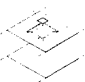
图3是本发明半导体芯片封装体的结构示意图。FIG. 3 is a schematic structural view of a semiconductor chip package of the present invention.
图4是本发明半导体芯片封装体的结构剖视示意图。4 is a schematic cross-sectional view of the structure of the semiconductor chip package of the present invention.
【具体实施方式】【Detailed ways】
首先请参阅图3、图4所示,本发明的半导体芯片的高散热微小封装体包含:First please refer to Fig. 3 and shown in Fig. 4, the high heat dissipation tiny package body of the semiconductor chip of the present invention comprises:
一导线架1,该导线架1以蚀刻程序制作出一凹入的芯片座11的平台,在该芯片座11四周设为镂空的镂空槽孔13仅留有数片支撑带12连接至导线架主体;A lead frame 1, the lead frame 1 produces a platform of a
一基板3,该基板3可应用于高密度线路的制作,以达到高脚数的需求,该基板3贴合于该导线架1下方,该基板3上设有高密度线路及多数脚垫31及锡球32,并将该脚垫31制作于相对于导线架1的镂空槽孔13位置,以接合金线22;A
一芯片2,该芯片2以接合剂23正向接合于导线架1的芯片座11上,并以打线技术将金线22打在芯片脚垫21与基板3上的预留脚垫31上,以达到其功能输出的目的,且该芯片2运作时产生的热量可藉由芯片座11经支撑带12传导到导线架1的其他区域散发,达到高散热的功能;A
根据上述结构将导线架1与基板3接合后,将芯片2接合于导线架1的芯片座11上,并以打线技术将芯片脚垫21与基板3的脚垫31及表面植设的锡球32间以金线22连接导通,最后以封胶4填于镂空槽孔13并包覆金线22与导线架1的部分表面区域。After the lead frame 1 is bonded to the
综上所述,本发明以微型封装技术将导线架与基板结合一体,使整体封装体可不需使用铜板或用散热板而达到超薄形态,同时兼可满足高脚数需求;芯片运作时产生的热量可藉由导线架传导出去,以达高散热的功效。To sum up, the present invention integrates the lead frame and the substrate with micro-packaging technology, so that the overall package can achieve an ultra-thin shape without using a copper plate or a heat sink, and at the same time can meet the demand for a high number of pins; The heat can be conducted out through the lead frame to achieve high heat dissipation effect.
Claims (1)
Priority Applications (1)
| Application Number | Priority Date | Filing Date | Title |
|---|---|---|---|
| CNA021431965A CN1484302A (en) | 2002-09-17 | 2002-09-17 | High heat dissipation micro package of semiconductor chip |
Applications Claiming Priority (1)
| Application Number | Priority Date | Filing Date | Title |
|---|---|---|---|
| CNA021431965A CN1484302A (en) | 2002-09-17 | 2002-09-17 | High heat dissipation micro package of semiconductor chip |
Publications (1)
| Publication Number | Publication Date |
|---|---|
| CN1484302A true CN1484302A (en) | 2004-03-24 |
Family
ID=34148207
Family Applications (1)
| Application Number | Title | Priority Date | Filing Date |
|---|---|---|---|
| CNA021431965A Pending CN1484302A (en) | 2002-09-17 | 2002-09-17 | High heat dissipation micro package of semiconductor chip |
Country Status (1)
| Country | Link |
|---|---|
| CN (1) | CN1484302A (en) |
Cited By (6)
| Publication number | Priority date | Publication date | Assignee | Title |
|---|---|---|---|---|
| CN100378933C (en) * | 2005-03-14 | 2008-04-02 | 日月光半导体制造股份有限公司 | Method for manufacturing semiconductor packaging structure with laminated crystal cavity |
| CN100433278C (en) * | 2004-10-29 | 2008-11-12 | 矽品精密工业股份有限公司 | Heat dissipation type packaging structure and manufacturing method thereof |
| CN100490103C (en) * | 2006-07-11 | 2009-05-20 | 日月光半导体制造股份有限公司 | Method for manufacturing substrate welding cover layer and structure thereof |
| CN100530624C (en) * | 2006-08-07 | 2009-08-19 | 南茂科技股份有限公司 | Method for packaging lead frame substrate ball grid array |
| CN110446369A (en) * | 2019-07-23 | 2019-11-12 | 中国科学技术大学 | Bonding structure, bonding method, and packaging box containing the same |
| CN110446368A (en) * | 2019-07-23 | 2019-11-12 | 中国科学技术大学 | Bonding structure, bonding method, and packaging box containing the same |
-
2002
- 2002-09-17 CN CNA021431965A patent/CN1484302A/en active Pending
Cited By (7)
| Publication number | Priority date | Publication date | Assignee | Title |
|---|---|---|---|---|
| CN100433278C (en) * | 2004-10-29 | 2008-11-12 | 矽品精密工业股份有限公司 | Heat dissipation type packaging structure and manufacturing method thereof |
| CN100378933C (en) * | 2005-03-14 | 2008-04-02 | 日月光半导体制造股份有限公司 | Method for manufacturing semiconductor packaging structure with laminated crystal cavity |
| CN100490103C (en) * | 2006-07-11 | 2009-05-20 | 日月光半导体制造股份有限公司 | Method for manufacturing substrate welding cover layer and structure thereof |
| CN100530624C (en) * | 2006-08-07 | 2009-08-19 | 南茂科技股份有限公司 | Method for packaging lead frame substrate ball grid array |
| CN110446369A (en) * | 2019-07-23 | 2019-11-12 | 中国科学技术大学 | Bonding structure, bonding method, and packaging box containing the same |
| CN110446368A (en) * | 2019-07-23 | 2019-11-12 | 中国科学技术大学 | Bonding structure, bonding method, and packaging box containing the same |
| CN110446368B (en) * | 2019-07-23 | 2024-07-26 | 中国科学技术大学 | Bonding structure, bonding method and packaging box containing bonding structure |
Similar Documents
| Publication | Publication Date | Title |
|---|---|---|
| TW498516B (en) | Manufacturing method for semiconductor package with heat sink | |
| US6369448B1 (en) | Vertically integrated flip chip semiconductor package | |
| US6657311B1 (en) | Heat dissipating flip-chip ball grid array | |
| US7554185B2 (en) | Flip chip and wire bond semiconductor package | |
| TW502417B (en) | Chip-embedded-type semiconductor package with high heat dissipation | |
| CN1221027C (en) | Semiconductor package with heat dissipation structure | |
| JP5227501B2 (en) | Stack die package and method of manufacturing the same | |
| WO2023098545A1 (en) | Packaging structure for large-current power semiconductor device and packaging method therefor | |
| US7235870B2 (en) | Microelectronic multi-chip module | |
| TWI321838B (en) | Stacked type chip package, chip package and process thereof | |
| TWI231017B (en) | Heat dissipation apparatus for package device | |
| JPH04123441A (en) | Semiconductor integrated circuit device | |
| CN1484302A (en) | High heat dissipation micro package of semiconductor chip | |
| US6770513B1 (en) | Thermally enhanced flip chip packaging arrangement | |
| TW200601534A (en) | Leadframe for multi-chip package and method for manufacturing the same | |
| JPH0878618A (en) | Multi-chip module and manufacturing method thereof | |
| TWI230449B (en) | High heat dissipation micro package of semiconductor chip | |
| CN100411121C (en) | Heat dissipation type package structure and manufacturing method thereof | |
| CN100524736C (en) | Stacked chip package structure | |
| JP3628991B2 (en) | Semiconductor device and manufacturing method thereof | |
| CN1790693A (en) | Flip chip and wire bond semiconductor package | |
| JPH08250628A (en) | Semiconductor integrated circuit device and manufacturing method thereof | |
| JPH11238828A (en) | Semiconductor device of BGA type package, method of manufacturing the same, and mounting device | |
| JPH02291154A (en) | Ceramic package provided with heat sink | |
| CN100433278C (en) | Heat dissipation type packaging structure and manufacturing method thereof |
Legal Events
| Date | Code | Title | Description |
|---|---|---|---|
| C06 | Publication | ||
| PB01 | Publication | ||
| C10 | Entry into substantive examination | ||
| SE01 | Entry into force of request for substantive examination | ||
| C02 | Deemed withdrawal of patent application after publication (patent law 2001) | ||
| WD01 | Invention patent application deemed withdrawn after publication |