CN1517455A - Laser recrystallization method - Google Patents
Laser recrystallization method Download PDFInfo
- Publication number
- CN1517455A CN1517455A CNA031015816A CN03101581A CN1517455A CN 1517455 A CN1517455 A CN 1517455A CN A031015816 A CNA031015816 A CN A031015816A CN 03101581 A CN03101581 A CN 03101581A CN 1517455 A CN1517455 A CN 1517455A
- Authority
- CN
- China
- Prior art keywords
- amorphous silicon
- laser
- silicon island
- energy density
- stage
- Prior art date
- Legal status (The legal status is an assumption and is not a legal conclusion. Google has not performed a legal analysis and makes no representation as to the accuracy of the status listed.)
- Granted
Links
- 238000000034 method Methods 0.000 title claims abstract description 155
- 238000001953 recrystallisation Methods 0.000 title claims abstract description 75
- 229910021417 amorphous silicon Inorganic materials 0.000 claims abstract description 117
- 239000000758 substrate Substances 0.000 claims abstract description 33
- 229910021420 polycrystalline silicon Inorganic materials 0.000 claims abstract description 22
- XUIMIQQOPSSXEZ-UHFFFAOYSA-N Silicon Chemical group [Si] XUIMIQQOPSSXEZ-UHFFFAOYSA-N 0.000 claims abstract description 7
- 230000001678 irradiating effect Effects 0.000 claims abstract 6
- 229920005591 polysilicon Polymers 0.000 claims description 20
- 239000013078 crystal Substances 0.000 claims description 13
- 239000011521 glass Substances 0.000 claims description 11
- 229910021419 crystalline silicon Inorganic materials 0.000 claims description 6
- 238000004518 low pressure chemical vapour deposition Methods 0.000 claims description 6
- 238000000623 plasma-assisted chemical vapour deposition Methods 0.000 claims description 6
- 230000008018 melting Effects 0.000 claims description 5
- 238000002844 melting Methods 0.000 claims description 5
- 238000004544 sputter deposition Methods 0.000 claims description 5
- 239000010453 quartz Substances 0.000 claims description 4
- VYPSYNLAJGMNEJ-UHFFFAOYSA-N silicon dioxide Inorganic materials O=[Si]=O VYPSYNLAJGMNEJ-UHFFFAOYSA-N 0.000 claims description 4
- 238000005280 amorphization Methods 0.000 claims 2
- 238000005530 etching Methods 0.000 claims 2
- 238000000206 photolithography Methods 0.000 claims 2
- 239000010409 thin film Substances 0.000 description 24
- 239000010408 film Substances 0.000 description 19
- 238000010586 diagram Methods 0.000 description 13
- 238000005516 engineering process Methods 0.000 description 12
- 238000005224 laser annealing Methods 0.000 description 11
- 239000004973 liquid crystal related substance Substances 0.000 description 8
- 230000006911 nucleation Effects 0.000 description 7
- 238000010899 nucleation Methods 0.000 description 7
- 238000004519 manufacturing process Methods 0.000 description 6
- 238000006243 chemical reaction Methods 0.000 description 4
- 238000005499 laser crystallization Methods 0.000 description 4
- 238000009826 distribution Methods 0.000 description 3
- 238000010521 absorption reaction Methods 0.000 description 2
- 230000015556 catabolic process Effects 0.000 description 2
- 238000002425 crystallisation Methods 0.000 description 2
- 230000008025 crystallization Effects 0.000 description 2
- 238000006731 degradation reaction Methods 0.000 description 2
- 238000013461 design Methods 0.000 description 2
- 238000011161 development Methods 0.000 description 2
- 206010016165 failure to thrive Diseases 0.000 description 2
- 238000010791 quenching Methods 0.000 description 2
- 230000000171 quenching effect Effects 0.000 description 2
- 229910052710 silicon Inorganic materials 0.000 description 2
- 239000010703 silicon Substances 0.000 description 2
- UFHFLCQGNIYNRP-UHFFFAOYSA-N Hydrogen Chemical compound [H][H] UFHFLCQGNIYNRP-UHFFFAOYSA-N 0.000 description 1
- 230000007547 defect Effects 0.000 description 1
- 238000000151 deposition Methods 0.000 description 1
- 238000005137 deposition process Methods 0.000 description 1
- 230000005284 excitation Effects 0.000 description 1
- 230000017525 heat dissipation Effects 0.000 description 1
- 229910052739 hydrogen Inorganic materials 0.000 description 1
- 239000001257 hydrogen Substances 0.000 description 1
- 229910044991 metal oxide Inorganic materials 0.000 description 1
- 150000004706 metal oxides Chemical class 0.000 description 1
- 238000012986 modification Methods 0.000 description 1
- 230000004048 modification Effects 0.000 description 1
- 238000012827 research and development Methods 0.000 description 1
- 239000004065 semiconductor Substances 0.000 description 1
- 230000003746 surface roughness Effects 0.000 description 1
- 238000003852 thin film production method Methods 0.000 description 1
- 230000000007 visual effect Effects 0.000 description 1
Images



Landscapes
- Recrystallisation Techniques (AREA)
Abstract
本发明先于基底之上形成至少一非晶硅岛,然后依序进行第一阶段以及第二阶段的激光再结晶制程,即先利用具有第一能量密度的激光脉冲照射该非晶硅岛,以使该非晶硅岛的边缘部分再结晶成为多晶硅结构,接着再利用具有第二能量密度的激光脉冲照射该非晶硅岛,以使该非晶硅岛的中央部分再结晶成为多晶硅结构。

The present invention first forms at least one amorphous silicon island on a substrate, and then sequentially performs a first stage and a second stage of laser recrystallization processes, that is, firstly irradiating the amorphous silicon island with a laser pulse having a first energy density so that the edge portion of the amorphous silicon island is recrystallized into a polycrystalline silicon structure, and then irradiating the amorphous silicon island with a laser pulse having a second energy density so that the central portion of the amorphous silicon island is recrystallized into a polycrystalline silicon structure.
Description
技术领域technical field
本发明是提供一种激光再结晶(laser crystallization,LC)的方法,尤指一种可以增大制程范畴(process window)的两阶段(two steps)的激光再结晶的方法。The present invention provides a laser recrystallization (laser crystallization, LC) method, especially a two-step laser recrystallization method that can increase the process window.
背景技术Background technique
在现今平面显示器的产品中,液晶显示器(liquid crystal display,LCD)可谓其中最为热门的一项技术,举凡日常生活中常见的手机、数码相机、摄影机、笔记本电脑以至于监视器均是利用此项技术所制造的商品。随着人们对于显示器视觉感受要求的提高,加上新技术应用领域不断的扩展,更高画质、高解析度、高亮度且具低价位的平面显示器便成为未来显示技术发展的趋势,也造就了新的显示技术发展的原动力。而平面显示器中的低温复晶硅薄膜晶体管(low temperature polysilicon thin film transistor,LTPSTFT)液晶显示器(LCD)除了具有符合主动式驱动(actively drive)潮流的特性外,其技术也正是一个可以达到上述目标的重要技术突破。尤其是其具有将金属氧化物半导体以及低温复晶硅薄膜晶体管整合(integrated)于同一制程技术的优点,使系统面板(system on panel,SOP)的目标得以被实现,因此成为各家厂商所积极研究发展的对象。In today's flat panel display products, liquid crystal display (LCD) is one of the most popular technologies, which are used in mobile phones, digital cameras, video cameras, notebook computers and even monitors that are common in daily life. Goods produced by technology. With the improvement of people's requirements for display visual experience and the continuous expansion of new technology application fields, flat-panel displays with higher image quality, high resolution, high brightness and low price will become the trend of future display technology development. Created the driving force behind the development of new display technology. The low temperature polysilicon thin film transistor (LTPSTFT) liquid crystal display (LCD) in the flat panel display has the characteristics of conforming to the trend of active drive (actively drive), and its technology is also a technology that can achieve the above-mentioned An important technological breakthrough for the target. In particular, it has the advantages of integrating metal oxide semiconductors and low-temperature polysilicon thin film transistors into the same process technology, so that the goal of system on panel (SOP) can be realized, so it has become an active goal of various manufacturers. object of research and development.
但是在低温复晶硅薄膜晶体管液晶显示器的制作过程中,由于一般玻璃基板的耐热度只能到600℃左右,若在高温下直接制作多晶硅薄膜将会造成玻璃基板的扭曲变形,因此传统的多晶硅薄膜晶体管液晶显示器往往必须要使用价格昂贵的石英作为基材,应用范围因而也只能局限于小尺寸的液晶面板。目前另一种利用非晶硅薄膜(amorphous silicon,α-Si thin film)再结晶的低温多晶硅薄膜制作方法已应运而生并且成为主流,其中又以受激准分子激光退火(excimer laser annealing,ELA)制程格外受到重视。However, in the production process of low-temperature polysilicon thin film transistor liquid crystal display, since the heat resistance of the general glass substrate can only reach about 600°C, if the polysilicon film is directly fabricated at high temperature, the glass substrate will be distorted and deformed. Therefore, the traditional Polysilicon thin-film transistor liquid crystal displays often have to use expensive quartz as the substrate, so the scope of application can only be limited to small-sized liquid crystal panels. At present, another low-temperature polysilicon thin film production method using amorphous silicon thin film (a-Si thin film) recrystallization has emerged and has become the mainstream. Among them, excimer laser annealing (excimer laser annealing, ELA ) process has received special attention.
请参考图1,图1为以受激准分子激光退火制程制作多晶硅薄膜的方法示意图。如图1所示,首先在玻璃基板10上沉积厚度约为500埃()的非晶硅薄膜12,接着将玻璃基板10置入一密闭的反应室(未显示)内,以进行受激准分子激光退火制程。其中,沉积非晶硅薄膜12的方法有许多种,诸如低压化学气相沉积(LPCVD)、等离子体辅助化学气相沉积(PECVD)及溅射(sputtering)等,而在进行该受激准分子激光退火制程时,受激准分子激光的激光脉冲14可自反应室(未显示)上方的透明窗口(未显示)照射至玻璃基板10表面的非晶硅薄膜12,并根据预先设定的制程范围以一种类似扫描(scan)的方式逐步扫过该制程范围内的所有区域,来对该制程范围内的非晶硅薄膜12进行快速加热,使其再结晶(recrystallize)成多晶硅薄膜(polysilicon thinfilm,未显示)。Please refer to FIG. 1 . FIG. 1 is a schematic diagram of a method for fabricating a polysilicon thin film by an excimer laser annealing process. As shown in Figure 1, at first on the
由于在受激准分子激光退火过程中,非晶硅薄膜会经由对激光深紫外光的吸收而达到快速的熔融与再结晶,而且采用这种短时间脉冲激光所造成的快速吸收只会对非晶硅薄膜表面造成影响,所以玻璃基板能保持在低温状态而不至受到任何影响。一般而言,常用的受激准分子激光种类包含有XeCl激光、ArF激光、KrF激光以及XeF激光等,不同的分子会产生不同的波长,而所输出的能量密度(energy density)则会根据非晶硅薄膜的厚度调整,以一个厚度500埃的非晶硅薄膜为例,受激准分子激光输出的能量密度约为200至400mJ/cm2。在完成该受激准分子激光退火制程之后,便可进一步进行后续液晶显示面板的其余制程,利用该多晶硅薄膜作为液晶显示器内的通道(source)或是源极/漏极(source/drain),以构成液晶显示器面板中的驱动电路(driving circuit)或是逻辑电路(logic circuit)。Because in the process of excimer laser annealing, the amorphous silicon thin film will achieve rapid melting and recrystallization through the absorption of laser deep ultraviolet light, and the rapid absorption caused by this short-time pulse laser will only affect non-crystalline silicon. The surface of the crystalline silicon film is affected, so the glass substrate can be kept at a low temperature without being affected. Generally speaking, the commonly used types of excimer lasers include XeCl laser, ArF laser, KrF laser and XeF laser, etc. Different molecules will produce different wavelengths, and the output energy density will be based on different The thickness adjustment of the crystalline silicon film, taking an amorphous silicon film with a thickness of 500 angstroms as an example, the energy density output by the excimer laser is about 200 to 400 mJ/cm 2 . After the excimer laser annealing process is completed, the rest of the subsequent liquid crystal display panel process can be further carried out, using the polysilicon film as the channel (source) or source/drain (source/drain) in the liquid crystal display, To form a driving circuit or a logic circuit in a liquid crystal display panel.
如前所述,由于非晶硅薄膜12的品质好坏对后续所形成的多晶硅薄膜特性影响很大,因此非晶硅薄膜沉积制程中的各参数(parameter)需要被严格控制,以期能形成低氢含量(hydrogen content)、高膜厚均匀性(thicknessuniformity)以及低表面粗糙度(surface roughness)的非晶硅薄膜。另外在非晶硅薄膜12再结晶成为多晶硅薄膜的过程中,也有许多的变数(variables)会对再结晶完成后的晶粒大小(grain size)以及分布(distribution)有直接的影响,而当激光结晶过程中产生不均匀的现象时,常会产生各式各样的缺陷(defect)。As mentioned above, since the quality of the
请参考图2,图2为已知技术中进行激光再结晶制程的能量密度示意图。如图2所示,利用已知技术进行激光再结晶制程时,所选择的激光能量密度E是介于近乎完全熔融能量密度(nearly-completely-melted energydensity,ENCM)以及超级侧向成长能量密度(SLG energy density,ESLG)之间。由图2中可以明显地看到,当激光能量密度小于近乎完全熔融能量密度时,由于能量密度不足以供给晶种(seed)成长成为大晶粒(large grain),故所形成的晶粒较小;当能量密度大于非晶硅化能量密度(amorphousization energydensity,Eα)时,虽然非晶硅薄膜12可以被完全熔融,但是结晶的方式是以淬冷的方式所达成,所以形成均匀形核(homogeneous nucleation)的现象,也因为均匀形核的缘故而到处都会产生成核点,晶粒无法有效成长,所以形成的晶粒大小会突然聚减,甚至还会非晶硅化;而当能量密度介于超级侧向成长能量密度以及非晶硅化能量密度之间时,虽然仍然可以形成大晶粒,但是小晶粒也开始被产生,往往造成不同元件之间(device to device)晶粒大小的均匀性(uniformity)无法被良好控制的情形,进而造成不同元件之间电性的差异。Please refer to FIG. 2 , which is a schematic diagram of the energy density of the laser recrystallization process in the prior art. As shown in Figure 2, when using known technology for laser recrystallization process, the selected laser energy density E is between the near-completely-melted energy density ( ENCM ) and the super lateral growth energy density (SLG energy density, E SLG ). It can be clearly seen from Figure 2 that when the energy density of the laser is less than the energy density of nearly complete melting, since the energy density is not enough to supply the seed crystal (seed) to grow into a large grain (large grain), the formed grains are relatively small. small; when the energy density is greater than the amorphous siliconization energy density (amorphousization energydensity, E α ), although the
然而已知用来激光再结晶的方法,却存在极大的限制。请参考图3A与图3B,图3A与图3B为已知技术中对非晶硅岛20A、20B进行激光再结晶后的剖面结果示意图。由于通常在实际的制作过程中,在形成非晶硅层12之后,还包括黄光暨蚀刻制程(photo-etching-process,PEP,未显示),以将非晶硅薄膜12蚀刻成为如图3A或者图3B所示的非晶硅岛(amorphous siliconisland)20A、20B。非晶硅岛20A、20B依制程以及设计的需要,可能具有不同的形状(shape),而在图3A以及图3B中是以最常见的用来作为低温复晶硅薄膜晶体管(未显示)的主动区域(active area)的情形来说明。Known methods for laser recrystallization, however, have significant limitations. Please refer to FIG. 3A and FIG. 3B . FIG. 3A and FIG. 3B are schematic cross-sectional views of amorphous silicon islands 20A and 20B after laser recrystallization in the prior art. Since usually in the actual manufacturing process, after forming the
如图3A以及图3B所示,由于散热方向多少的不同,其边缘部分22A、22B的热传导速率(thermal conduction rate)大于其中央部分24A、24B的热传导速率,进而形成温度梯度(temperature gradient),因此非晶硅岛20A、20B边缘部分22A、22B的非晶硅薄膜在达到近乎完全熔融状态之后先行固化(solidify)),再由位于边缘部分22A、22B的非晶硅薄膜内的残余(residual)非晶硅晶种(seed,未显示)向中央部分24A、24B做侧向成长(lateral grow)成为大晶粒(large grain)26A、26B。但无论如何,侧向成长的速度有一定的极限,通常只能成长到1~2微米(μm)。如图3A所示,当元件的通道宽度(channelwidth)较小时,大晶粒26A可以成长到线宽(channel width)的中央,因此可以改善元件的电性。所以此已知先形成非晶硅岛再激光结晶的方法,有时会选用高于ESLG的能量密度,以增加侧向成长的驱动力。但是如图3B所示,当元件的通道宽度较大时,会造成只有在边缘部分22B长成大晶粒26B,却在中央部分24B长成小晶粒28的现象,最后造成元件电性的劣化(degrade)。As shown in FIG. 3A and FIG. 3B , due to the somewhat different heat dissipation directions, the thermal conduction rate (thermal conduction rate) of the edge portions 22A, 22B is greater than that of the central portion 24A, 24B, thereby forming a temperature gradient. Therefore, the amorphous silicon film of the edge portions 22A, 22B of the amorphous silicon islands 20A, 20B first solidifies (solidify) after reaching a nearly completely molten state, and then the residual (residual) in the amorphous silicon film located at the edge portions 22A, 22B ) amorphous silicon seeds (seed, not shown) grow laterally toward the central portions 24A, 24B to become large grains 26A, 26B. But in any case, the speed of lateral growth has a certain limit, and usually only grows to 1-2 microns (μm). As shown in FIG. 3A , when the channel width of the device is small, the large grain 26A can grow to the center of the channel width, thereby improving the electrical properties of the device. Therefore, in the known method of first forming amorphous silicon islands and then laser crystallization, energy density higher than E SLG is sometimes selected to increase the driving force of lateral growth. But as shown in FIG. 3B, when the channel width of the element is large, only the large crystal grain 26B grows in the edge part 22B, but grows into the phenomenon of the small crystal grain 28 in the central part 24B, and finally causes the element electrical property Degrade.
同时已知技术中所使用的激光能量密度范围太小,当激光能量密度的大小稍有误差时,很容易就超出了上述的激光能量密度范围。甚至于当激光能量空间上分布的均匀性、激光脉冲(pulse)的重叠(overlap)程度、进行激光退火时基板的温度以及周围的气氛(atmosphere)等变数(variable)未被控制妥当时,也会相对造成所使用的激光能量密度超出上述的激光能量密度范围。At the same time, the laser energy density range used in the known technology is too small, and when there is a slight error in the size of the laser energy density, it is easy to exceed the above laser energy density range. Even when variables such as the uniformity of the spatial distribution of laser energy, the degree of overlap of laser pulses, the temperature of the substrate during laser annealing, and the surrounding atmosphere (atmosphere) are not properly controlled, the It will relatively cause the laser energy density used to exceed the above laser energy density range.
因此,如何能研究出一种新的激光再结晶的方法,其不仅可以促进非晶硅岛各个部位的有效侧向成长,以形成均匀的大晶粒,并且又可以增大激光再结晶制程的制程范畴(process window),便成为十分重要的课题。Therefore, how can a new laser recrystallization method be developed, which can not only promote the effective lateral growth of each part of the amorphous silicon island to form uniform large grains, but also increase the laser recrystallization process. The process window has become a very important issue.
发明内容Contents of the invention
本发明的主要目的在于提供一种激光再结晶(laser crystallization,LC)制程的方法,尤指一种可以明显增大制程范畴(process window)的两阶段激光再结晶的方法。The main purpose of the present invention is to provide a laser recrystallization (laser crystallization, LC) process method, especially a two-stage laser recrystallization method that can significantly increase the process window.
在本发明的最佳实施例中,先提供基底,再在该基底之上形成至少一非晶硅岛,然后进行第一阶段的激光再结晶制程,利用具有第一能量密度的激光脉冲照射该非晶硅岛(amorphous silicon island,α-Si island),以使该非晶硅岛的边缘部分再结晶成为侧向成长多晶硅结构(lateral growthpolysilicon structure),接着进行第二阶段的激光再结晶制程,利用具有第二能量密度(second energy density)的激光脉冲照射该非晶硅岛,以使该非晶硅岛的中央部分(center portion)再结晶成为多晶硅结构。In a preferred embodiment of the present invention, a substrate is provided first, and then at least one amorphous silicon island is formed on the substrate, and then the first-stage laser recrystallization process is performed, and the laser pulse with the first energy density is used to irradiate the substrate. Amorphous silicon island (α-Si island), so that the edge part of the amorphous silicon island is recrystallized into a lateral growth polysilicon structure (lateral growth polysilicon structure), followed by the second stage of laser recrystallization process, The amorphous silicon island is irradiated with laser pulses having a second energy density to recrystallize a center portion of the amorphous silicon island into a polysilicon structure.
由于本发明的激光再结晶的方法是利用两阶段式的激光再结晶制程(laser crystallization,process,LC process),先将非晶硅岛的边缘部分再结晶成为大晶粒,然后再将非晶硅岛的中央部分内的小晶粒修补成为大晶粒。即使当非晶硅岛是应用于通道宽度较大的元件时,也不会产生当晶粒向非晶硅岛的中央部分侧向成长时,由于侧向成长的速度有极限而产生的无法成长到线宽的中央的情形,因此可以充分避免元件的电性被劣化。同时,因为在第二阶段的激光再结晶制程时只需顾虑到非晶硅岛的中央部分,本发明的激光再结晶方法的制程范畴可以明显被增大,不至于因为激光能量密度的大小稍有误差,或是激光再结晶制程中的其他变数未被控制妥当,便很容易地超出了制程的激光能量密度范围。利用本发明方法于实际生产线时,将可以制做出具有良好电性的大通道元件。Because the laser recrystallization method of the present invention utilizes a two-stage laser recrystallization process (laser crystallization, process, LC process), the edge portion of the amorphous silicon island is first recrystallized into large grains, and then the amorphous silicon The small dies within the central portion of the silicon islands are patched into large dies. Even when the amorphous silicon island is applied to a device with a large channel width, when the crystal grain grows laterally to the central part of the amorphous silicon island, there will be no growth failure due to the limit of the lateral growth speed. To the center of the line width, it is possible to fully avoid the electrical degradation of the element. At the same time, because only the central part of the amorphous silicon island needs to be considered during the laser recrystallization process in the second stage, the process scope of the laser recrystallization method of the present invention can be significantly increased, and it will not be caused by the size of the laser energy density. If there are errors, or other variables in the laser recrystallization process are not properly controlled, it is easy to exceed the laser fluence range of the process. When the method of the invention is used in an actual production line, large-channel components with good electrical properties can be produced.
附图说明Description of drawings
图1为以受激准分子激光退火制程制作多晶硅薄膜的方法示意图。FIG. 1 is a schematic diagram of a method for fabricating a polysilicon thin film by an excimer laser annealing process.
图2为已知技术中进行激光再结晶制程的能量密度示意图。FIG. 2 is a schematic diagram of the energy density of the laser recrystallization process in the prior art.
图3A与图3B为已知技术中对非晶硅岛进行激光再结晶后的剖面结果示意图。3A and 3B are schematic diagrams of cross-sectional results of amorphous silicon islands after laser recrystallization in the prior art.
图4至图5为本发明中进行激光再结晶的方法示意图。4 to 5 are schematic diagrams of the laser recrystallization method in the present invention.
图6A与图6B为本发明方法中对非晶硅岛进行激光再结晶后的剖面结果示意图。6A and 6B are schematic diagrams of cross-sectional results of amorphous silicon islands after laser recrystallization in the method of the present invention.
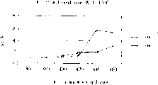
图7为利用本发明的激光再结晶方法所制作的N型薄膜晶体管的迁移率的示意图。FIG. 7 is a schematic diagram of the mobility of an N-type thin film transistor fabricated by the laser recrystallization method of the present invention.
图8为利用本发明的激光再结晶方法所制作的N型薄膜晶体管的起始电压的示意图。FIG. 8 is a schematic diagram of the initial voltage of an N-type thin film transistor fabricated by the laser recrystallization method of the present invention.
图示的符号说明Illustration of symbols
10玻璃基板 12非晶硅薄膜10
14激光脉冲 20A、20B非晶硅岛14 laser pulses 20A, 20B amorphous silicon island
22A、22B边缘部分 24A、24B中央部分22A, 22B edge part 24A, 24B central part
26A、26B大晶粒 28小晶粒26A, 26B large grains 28 small grains
100绝缘基板 102非晶硅岛100 insulating
103激光脉冲 104边缘部分103 laser pulses 104 edge parts
106中央部分 108大晶粒106 central part 108 large grains
111小晶粒 112 SLG晶粒111 small grains 112 SLG grains
具体实施方式Detailed ways
请参考图4至6B,图4至图5为本发明中进行激光再结晶的方法示意图,图6A至图6B为本发明方法中对非晶硅岛102进行激光再结晶后的剖面结果示意图。如图4所示,首先提供绝缘基板100,且绝缘基板100包括玻璃(glass)基板、石英(quartz)基板或者塑料(plastic)基板。接着于绝缘基板100之上形成非晶硅薄膜(amorphous silicon thin film,α-Si thin film,未显示),然后进行黄光暨蚀刻制程(photo-etching-process,PEP)以将非晶硅薄膜(未显示)蚀刻成为非晶硅岛(amorphous island)102。其中形成非晶硅薄膜(未显示)的方法包括低压化学气相沉积(LPCVD)制程、等离子体辅助化学气相沉积(PECVD)制程或者溅射(sputtering)制程。同时非晶硅岛102依制程以及设计的需要,可能具有不同的形状,而在图4中是以最常见的用来作为低温复晶硅薄膜晶体管(未显示)的主动区域(active area)的情形来说明。Please refer to FIGS. 4 to 6B . FIGS. 4 to 5 are schematic diagrams of the method for laser recrystallization in the present invention, and FIGS. 6A to 6B are schematic diagrams of cross-sectional results of
再将绝缘基板100置入一密闭的反应室(未显示)内,以进行受激准分子激光退火制程。在进行受激准分子激光退火制程时,受激准分子激光的激光脉冲103可自反应室(未显示)上方的透明窗口(未显示)照射至玻璃基板100表面的非晶硅岛102,并根据预先设定的制程范围以一种类似扫描(scan)的方式逐步扫过该制程范围内的所有区域,来对该制程范围内的非晶硅岛102进行快速加热。同时受激准分子激光包含有XeCl激光、ArF激光、KrF激光或者XeF激光。Then the insulating
本发明的激光再结晶方法是利用两阶段(two steps)的激光再结晶制程来对非晶硅岛102做处理。如图5所示,本发明方法在进行第一阶段(first step)的激光再结晶制程时,所选择的激光能量密度E1大于(higher than)非晶硅岛102的超级侧向成长能量密度(super lateral growth energy density,ESLG),而事实上,优选第一能量密度(first energy density)大于非晶硅岛102的非晶硅化能量密度(amorphousization energy density,Eα)。如图6A所示,由于非晶硅岛102边缘部分104的热传导速率大于中央部分106的热传导速率,当进行第一阶段的激光再结晶制程时,温度梯度便因而产生,此时非晶硅岛102的边缘部分(edge portion)1 04在达到完全熔融(completely-melted)状态之后先行固化(solidify),再由非晶硅岛102的边缘部分104内的至少一晶种(未显示)向非晶硅岛102的中央部分106做侧向成长(lateral grow)成为至少一大晶粒108。The laser recrystallization method of the present invention utilizes a two-step laser recrystallization process to process the
由于侧向成长的速度有一定的极限,最后大晶粒108的尺寸(size)大约为1~2微米(μm)。于此同时,非晶硅岛102的中央部分106在达到完全熔融状态之后,是以淬冷的方式来结晶,因为均匀形核(homogeneous nucleation)的缘故非晶硅岛102的中央部分106内到处都会产生成核点(nucleationsite),晶粒无法有效成长,所形成的晶粒大小会突然骤减,成为许多小晶粒111,甚至还会非晶硅化,无法有效再结晶(recrystalize)并维持(remain)于非晶硅结构(amorphous silicon structure,未显示)。Since the lateral growth speed has a certain limit, the final size of the large crystal grains 108 is about 1-2 micrometers (μm). At the same time, the central portion 106 of the
接着进行第二阶段的激光再结晶制程,本发明方法在进行第二阶段(second step)的激光再结晶制程时,所选择的激光能量密度E2不大于(notgreater than)非晶硅岛102的超级侧向成长能量密度,而事实上,优选第二能量密度介于(in between)非晶硅岛102的近乎完全熔融能量密度(nearly-completely-melted energy density,ENCM)以及超级侧向成长能量密度(super lateral growth energy density,ESLG)之间。Then carry out the laser recrystallization process of the second stage, when the method of the present invention carries out the laser recrystallization process of the second stage (second step), the selected laser energy density E 2 is not greater than (not greater than) the
如图6B所示,此时非晶硅岛102的中央部分106达到近乎完全熔融状态,因而使非晶硅岛102的中央部分106成长为正常SLG晶粒112(约0.2~0.5μm结晶大小)。而在边缘部分已经被形成的大晶粒,则几乎不受任何影响。因此,经过此二阶段的激光再结晶制程之后的非晶硅岛102,其微观结构(microstructure)为大晶粒108及正常SLG晶粒112所构成,同时其电性也获得了明显的改善。请参考图7与图8,图7为利用本发明的激光再结晶方法所制作的N型薄膜晶体管的迁移率(mobility)的示意图,图8为利用本发明的激光再结晶方法所制作的N型薄膜晶体管的起始电压(threshold voltage)的示意图。由图7至图8中可以看到,经过此二阶段的激光再结晶制程之后,不论是电子在通道中的迁移率或是N型薄膜晶体管的起始电压均获得相当程度的改善,尤其是当第一次的激光再结晶制程实施于高能量密度范围时,改善的幅度更为明显。As shown in FIG. 6B, at this time, the central portion 106 of the
由于本发明的激光再结晶制程的方法,是利用两阶段式的激光再结晶制程,以分别将非晶硅岛的边缘部分以及中央部分再结晶成为大晶粒。如此一来,已知技术中因为非晶硅岛的边缘部分以及中央部分的热传导速率不同以及侧向成长的速度有极限而衍生的晶粒无法成长到线宽的中央的情形,将可以被有效避免。并且于第二阶段的激光再结晶制程时只需考虑到非晶硅岛的中央部分,本发明的激光再结晶方法的制程范畴将可以明显被增大,进而改善已知技术中当激光能量密度的大小稍有误差时,或当激光再结晶制程中的其他变数未被控制妥当时,便很容易地超出制程的激光能量密度范围的情形。利用本发明方法于实际生产线时,将可以生产出具有良好电性的大通道元件。The method of the laser recrystallization process of the present invention uses a two-stage laser recrystallization process to recrystallize the edge part and the central part of the amorphous silicon island into large grains respectively. In this way, the situation in the known technology that the grains derived from the amorphous silicon island cannot grow to the center of the line width due to the difference in heat conduction rate between the edge part and the central part and the limit of the lateral growth speed can be effectively utilized. avoid. And in the laser recrystallization process of the second stage, only the central part of the amorphous silicon island needs to be considered, and the process scope of the laser recrystallization method of the present invention can be significantly increased, thereby improving the laser energy density in the known technology When there is a slight error in the size of the laser recrystallization process, or when other variables in the laser recrystallization process are not properly controlled, it is easy to exceed the laser fluence range of the process. When the method of the invention is used in an actual production line, large-channel components with good electrical properties can be produced.
对于已知激光再结晶的方法,本发明的激光再结晶的方法是利用两阶段式的激光再结晶制程,先将非晶硅岛的边缘部分再结晶成为大晶粒,然后再将非晶硅岛的中央部分内的小晶粒修补成为正常晶粒。因此即使非晶硅岛是应用于通道宽度较大的元件时,也不会产生当晶粒向非晶硅岛的中央部分侧向成长时,由于侧向成长的速度有极限而产生的无法成长到线宽的中央的情形,进而避免元件的电性劣化的情形。同时,在进行第三阶段的激光再结晶制程时只需考虑到非晶硅岛的中央部分,本发明的激光再结晶方法的制程范畴可以明显被增大,不至于因为激光能量密度的大小稍有误差,便很容易地超出了制程的激光能量密度范围。此外,当激光再结晶制程中的其他变数未被控制妥当时,也相对较不容易造成所使用的激光能量密度超出制程的激光能量密度范围。For the known laser recrystallization method, the laser recrystallization method of the present invention utilizes a two-stage laser recrystallization process, first recrystallizes the edge part of the amorphous silicon island into large grains, and then recrystallizes the amorphous silicon Small grains within the central portion of the island are patched to become normal grains. Therefore, even if the amorphous silicon island is applied to a device with a large channel width, when the crystal grains grow laterally to the central part of the amorphous silicon island, there will be no growth failure due to the limit of the lateral growth speed. To the center of the line width, thereby avoiding the electrical degradation of the component. At the same time, only the central part of the amorphous silicon island needs to be considered when carrying out the laser recrystallization process in the third stage, and the process range of the laser recrystallization method of the present invention can be significantly increased, so that the laser recrystallization process will not be slightly affected by the laser energy density. If there is an error, it is easy to exceed the laser fluence range of the process. In addition, when other variables in the laser recrystallization process are not properly controlled, it is relatively less likely to cause the laser fluence used to exceed the laser fluence range of the process.
以上所述仅为本发明的优选实施例,凡依本发明权利要求所做的均等变化与修饰,皆应属本发明专利的涵盖范围。The above descriptions are only preferred embodiments of the present invention, and all equivalent changes and modifications made according to the claims of the present invention shall fall within the scope of the patent of the present invention.
Claims (24)
Priority Applications (1)
| Application Number | Priority Date | Filing Date | Title |
|---|---|---|---|
| CN 03101581 CN1246509C (en) | 2003-01-15 | 2003-01-15 | A method of laser crystallization |
Applications Claiming Priority (1)
| Application Number | Priority Date | Filing Date | Title |
|---|---|---|---|
| CN 03101581 CN1246509C (en) | 2003-01-15 | 2003-01-15 | A method of laser crystallization |
Publications (2)
| Publication Number | Publication Date |
|---|---|
| CN1517455A true CN1517455A (en) | 2004-08-04 |
| CN1246509C CN1246509C (en) | 2006-03-22 |
Family
ID=34281431
Family Applications (1)
| Application Number | Title | Priority Date | Filing Date |
|---|---|---|---|
| CN 03101581 Expired - Lifetime CN1246509C (en) | 2003-01-15 | 2003-01-15 | A method of laser crystallization |
Country Status (1)
| Country | Link |
|---|---|
| CN (1) | CN1246509C (en) |
Cited By (3)
| Publication number | Priority date | Publication date | Assignee | Title |
|---|---|---|---|---|
| CN103854975A (en) * | 2012-12-06 | 2014-06-11 | 三星显示有限公司 | Method of manufacturing poly-crystalline silicon layer, organic light-emitting display apparatus and method of manufacturing organic light-emitting display apparatus |
| CN105097940A (en) * | 2014-04-25 | 2015-11-25 | 上海和辉光电有限公司 | Thin film transistor array substrate structure and manufacturing method thereof |
| CN106033707A (en) * | 2015-03-10 | 2016-10-19 | 上海和辉光电有限公司 | Preparation method for polysilicon film |
-
2003
- 2003-01-15 CN CN 03101581 patent/CN1246509C/en not_active Expired - Lifetime
Cited By (4)
| Publication number | Priority date | Publication date | Assignee | Title |
|---|---|---|---|---|
| CN103854975A (en) * | 2012-12-06 | 2014-06-11 | 三星显示有限公司 | Method of manufacturing poly-crystalline silicon layer, organic light-emitting display apparatus and method of manufacturing organic light-emitting display apparatus |
| CN103854975B (en) * | 2012-12-06 | 2018-09-28 | 三星显示有限公司 | The manufacturing method and oganic light-emitting display device and its manufacturing method of polysilicon layer |
| CN105097940A (en) * | 2014-04-25 | 2015-11-25 | 上海和辉光电有限公司 | Thin film transistor array substrate structure and manufacturing method thereof |
| CN106033707A (en) * | 2015-03-10 | 2016-10-19 | 上海和辉光电有限公司 | Preparation method for polysilicon film |
Also Published As
| Publication number | Publication date |
|---|---|
| CN1246509C (en) | 2006-03-22 |
Similar Documents
| Publication | Publication Date | Title |
|---|---|---|
| US6391690B2 (en) | Thin film semiconductor device and method for producing the same | |
| US20030218215A1 (en) | Process for fabricating semiconductor device | |
| CN100474628C (en) | Method for annealing silicon thin films and polycrystalline silicon thin films prepared therefrom | |
| WO1997022142A1 (en) | Thin film semiconductor device, method for manufacturing thin film semiconductor device, liquid crystal display, method for manufacturing liquid crystal display, electronic apparatus, method for manufacturing electronic apparatus, and method for depositing thin film | |
| CN1213465C (en) | Method for making polycrystalline semiconductor layer and laser annealing device | |
| US7767558B2 (en) | Method of crystallizing amorphous silicon and device fabricated using the same | |
| US20120064702A1 (en) | Method of fabricating polycrystalline silicon thin film | |
| US7083676B2 (en) | Method of laser crystallization | |
| CN1246509C (en) | A method of laser crystallization | |
| JPH06283422A (en) | Polycrystalline semiconductor film, thin film using thereof, manufacturing method thereof | |
| KR100205069B1 (en) | Fabrication method of polysilicon thin film transistor | |
| CN1265428C (en) | A method of fabricating a thin film transistor | |
| JP3269730B2 (en) | Method of manufacturing semiconductor substrate and method of manufacturing semiconductor device | |
| KR100782769B1 (en) | Alignment key, alignment key formation method and laser crystallization method using the same | |
| KR100366960B1 (en) | silicon crystallization method | |
| CN1553474A (en) | Method for manufacturing polycrystalline silicon film by using excimer laser recrystallization process | |
| JPH0945926A (en) | Method for forming polycrystalline semiconductor thin film, thin film transistor, and method for manufacturing the same | |
| KR100333134B1 (en) | Crystallization method of amorphous silicon using electric field and UV | |
| US20030178682A1 (en) | Semiconductor device and method of manufacturing the semiconductor device | |
| JP4429598B2 (en) | Method for manufacturing semiconductor device | |
| CN1310282C (en) | Crystallization method of polysilicon layer | |
| JP3417182B2 (en) | Method for manufacturing thin film semiconductor device and method for manufacturing electronic equipment | |
| KR100504488B1 (en) | Method for Fabrication poly silicon thin film having low-temperrature using Metal Induced Crystalization method | |
| US7014708B2 (en) | Method of forming a thin film transistor by utilizing a laser crystallization process | |
| CN100388423C (en) | Method for manufacturing polycrystalline silicon thin film and thin film transistor obtained thereby |
Legal Events
| Date | Code | Title | Description |
|---|---|---|---|
| C06 | Publication | ||
| PB01 | Publication | ||
| C10 | Entry into substantive examination | ||
| SE01 | Entry into force of request for substantive examination | ||
| C14 | Grant of patent or utility model | ||
| GR01 | Patent grant | ||
| CX01 | Expiry of patent term |
Granted publication date: 20060322 |
|
| CX01 | Expiry of patent term |