A portion of the disclosure of this patent document contains material which is subject to copyright protection. The copyright owner has the permission of anyone to facsimile reproduction of the invention as it appears in the patent and trademark office patent files or records, but otherwise reserves all copyright rights whatsoever.
Detailed Description
A system and method for detecting biological and chemical materials is disclosed. Numerous specific limitations are set forth in order to provide a thorough understanding of the present invention. It will be understood by those skilled in the art that the present invention may be practiced without some or all of these specific limitations.
In the present specification, there is disclosed a structure of a small-sized measuring device having high sensitivity, having a probe for capturing biological materials such as nucleic acids and proteins immobilized on a chip, the measuring device being provided with a sensor, a functional block of an identification number and a radio frequency communication means, the sensor detecting the presence of a target captured on the probe and transmitting the sensing result to an external control unit through the radio frequency communication means. Also disclosed is a device for reading out an identification number and a sensor signal by a device for measuring an electromagnetic wave, a change in a magnetic field, or a change in an electric field.
(example 1)
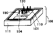
Fig. 1A illustrates a chemical measurement system using the biological and chemical material measurement apparatus 100 of the present invention. In the measuring apparatus 100, a probe 120 adapted to an object to be detected is fixed, a sensor 110 for detecting the object captured by the probe is mounted on the same substrate 111, a circuit block 102 having functions for processing sensor information, controlling communication with an external control unit 200, storing and matching identification numbers, and generating and controlling power supply, and an antenna 101 for communicating with the external control unit. Fig. 15A shows an example of using a shift register as a means for recording an identification number, and fig. 15B shows an example of integrating a clock-data separation circuit.
Fig. 1B shows a functional block diagram of the measurement apparatus 100. The measuring device 100 is placed in a sample container 300 containing a sample solution 301. In this measuring apparatus 100, a sensor 110 for detecting the presence and amount of a target object captured by a probe 120 partially or entirely immobilized on the surface of the measuring apparatus 100 is formed. In fig. 1, the probe is fixed only to the sensor area 110, but it may be partially or entirely fixed to the front and rear surfaces and the side portions of the measuring apparatus 100 other than the sensor area 100. Since the probe fixed on the protective film does not significantly affect the performance of the measuring apparatus, a protective film is coated on the surface of the measuring apparatus 100 except the sensing region 110. The signal detected by the sensor is converted into a digital electric signal by an AD converter (ADC) 107. At this time, it is reasonable from the design aspect of the integrated measuring device to set the resolution of the ADC to one (two values) -eight bits (256 values). When the resolution is set to one bit, the structure of the ADC is the same as that of a comparator, which is advantageous in terms of power consumption and chip occupation area. By setting to a larger number of bits, the sensor can obtain a high-resolution output, but power consumption and chip occupation area will also increase. On the other hand, the external control unit 200 transmits an identification number (0) for identifying a specific measuring device from among the plurality of measuring devices 100 by means of an electromagnetic wave 202 having a variation in magnetic field or electric field. The identification number is transmitted to the plurality of measuring devices in the sample container 300, and the antenna 101 mounted on each measuring device 100 receives the identification number, which is matched with the measuring device-specific identification number (1) written in advance in the measuring device 100 after passing through the shaping and demodulation circuit. Matching is performed in a matching circuit in the control circuit block 102 of each measurement device. When the identification number transmitted from the external control unit matches the identification number written in advance and finally determines a match, the matching-implementing measuring device transmits a matching signal to the external control unit 1 for reading through the communication control/signal processing circuit block 104 and the modulation circuit block 103 via the antenna 10 by means 203 of a change in electromagnetic waves, magnetic fields, or electric fields. When transmitted to the outside as electromagnetic waves, received through the antenna 101, or there is a change in the magnetic or electric field, the energy consumed by the control circuit block 102 and the sensor is provided by a DC power supply and voltage regulator including a rectifying and smoothing circuit in the control module.
(example 2)
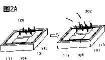
Referring to FIG. 2, a probe secured to a measurement device 100 is shown according to one aspect of the present invention. In FIG. 2A, a fragment of nucleic acid is used as a probe. Synthetic oligo-DNA and cDNA can be used as nucleic acid. In FIG. 2B, an example is given in which a protein or an antibody is used as a probe. In fig. 2C, an antigen is used as a probe.
(example 3)
For a sensor mounted on the measuring device 100, as shown in fig. 3, a type for measuring physical and chemical quantities in a position where the device is located may be used instead of the type of binding achieved by affinity of a probe with a target in a sample solution using a probe as shown in fig. 1. For example, sensors for measuring temperature, pressure, amount of light, pH, ion concentration, or sugar may be used.
In measuring the temperature, the temperature dependence of the semiconductor resistivity or the diode voltage-voltage characteristic can be utilized. In measuring pressure, a sensor of a micro-vibrating membrane structure implemented using a piezoelectric element or MEMS (micro electro mechanical system) technology may be used. In measuring the amount of light, a photosensor using a photodiode or a change in conductivity of a semiconductor caused by a light-excited carrier wave can be used. In measuring the pH value and the ion concentration, an ion-sensitive film that captures ions to change an electromotive force may be used.
After the physical and chemical quantities measured by the above-described sensors are converted into electric signals by a method and apparatus similar to those described in embodiment 1, they are digitized, modulated, and transmitted from the measuring apparatus 100 according to the identification number transmitted from the external control unit.
(example 4)
In the present embodiment, a substrate for the measurement apparatus 100 is explained. The measurement device includes functional blocks including a sensor, an antenna, a detection circuit, a rectification/modulation/demodulation circuit, and a communication/data processing/storage control circuit. By integrating these functional blocks on one chip, a small and lightweight measuring device can be realized while reducing the manufacturing and mounting costs. This type of functionality can also be achieved by mounting parts of the functional blocks on separate chips and integrating these chips on one printed circuit board.
When the above functional blocks are mounted on the same substrate, a silicon substrate may be used.
As shown in fig. 4A, the use of a silicon substrate enables the mounting of the elements and structures forming the above-described functional blocks using conventional, known techniques. The functional blocks of the rectifying/modulating/demodulating circuit and the data processing/storing circuit may be realized by integrated circuit technology using CMOS transistors.
Fig. 4B shows an insulating substrate 114, such as glass, quartz, and ceramic, to which a very thin silicon film is applied. For example, a polycrystalline silicon thin film may be plated on a sapphire substrate by a CVD (chemical vapor deposition) process and re-spread by a zone melting process to obtain a single crystal silicon thin film.
In fig. 4C, an intermediate layer is formed between the silicon thin film and the substrate. Single crystal silicon and ceramics can be used as the substrate. For example, by such a structure using single crystal Silicon as a substrate and SOI (Silicon on insulator) using a SiO2 thin film as an intermediate layer, any parasitic capacitance in the source, gate, and wiring of a MOS transistor can be reduced, thereby reducing power consumption. Therefore, it is sufficient to externally supply a small amount of energy, which can reduce the size of the antenna mounted on the measurement apparatus 100.
In this case, the length of the longest side of the measuring apparatus 100 is preferably not more than 3 mm. By making the measuring device smaller, the length of the microtiter plate or tube can be made 100. mu.l.
(example 5)
One aspect of a sensor mounted on a measuring device 100 according to the present invention is described below.
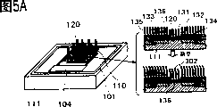
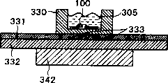
Fig. 5A shows an example of a sensor using a Field Effect Transistor (FET). The FET having the MOS structure is mounted on a silicon substrate 111. This means that the source region 133 is separated from the drain region 134 by a gate region including a gate electrode 131 made of a conductive material and a gate insulating film 132. A probe 120 is fixed to the gate electrode. Assuming that the target is a DNA fragment, when the target 302 is captured by the probe 120 by hybridization, the potential of the electrode will change as the DNA is negatively charged and affects the conductivity of the FET channel region 136. According to the method disclosed in Journal of Physical Chemistry B.101 (1997) at page 2980-2985 of south and, E.et al, the probe is immobilized at least in the region containing the gate electrode and hybridized in a sample solution, and the measurement of the conductivity between the source electrode 133 and the drain electrode 134 makes it possible to determine whether or not the target is bound to the probe 120 and the amount of the target.
The present invention relates to a system for detecting biological materials, such as genes, for which a sample preparation process is required. The sample DNA can be obtained by, for example, extracting a genome from blood and amplifying a plurality of target regions to be measured by PCR. The sample preparation method is not limited to the embodiments described in the present specification.
The probe can be immobilized by the following method. Glycidoxypropyl groups are introduced to the surface of the measurement device 100, which is covered with a protective film of SiO2 by a known silane bonding reaction. The measuring device 100 was immersed in a 1M NaOH solution and cleaned with ultrasonic waves for 30 minutes. After washing with purified running water, the measuring device100 was baked at a temperature of 110 ℃ for 15 minutes. The measuring apparatus was immersed in a concentrated 3-glycidoxypropyltrimethoxysilane solution for 5 minutes, and then immersed in a 4% 3-glycidoxypropyltrimethoxysilane solution dissolved in a 50% ethanol solution for 30 minutes with no stirring. The measuring device was baked at a temperature of 110 ℃ for 30 minutes to obtain a measuring device 100 having a glycidoxy group introduced with a silane coupling agent on its surface. Mu.l of different probes 120(20 pmol/. mu.l) suitable for the target to be measured were dissolved in 0.5M sodium bicarbonate buffer (pH 9.5) to obtain 1 pmol/. mu.l solutions. The measuring device 100 with the introduced glycidoxy group was immersed in the resulting solution. The measuring device 100 is heated at 50 ℃ for 30 minutes in an environment of saturated water vapor to avoid drying. The measurement device 100 was removed from the DNA solution and then immersed in 0.5M sodium bicarbonate buffer (pH 9.5) containing 0.1M Lys to block the remaining glycoxy groups. The measuring apparatus 100 was washed with 20mM Tris-HCl (pH 7.5). By the above-mentioned treatment, the probe 120 containing several hundreds of kinds of probes is immobilized by the reaction between the amino group at the 5' end and the glycidoxy group. As the probe, for example, the following synthetic oligo-DNA can be used.
[ wild-type p53 exon 8]
5’-CAG GACAG GCACA AACAC GCACC TCAAA G-
3' (SEQ ID NO: 1)
The following oligo-DNA was used as a target corresponding to the above probe.
5’-
AACAGCTTTGAGGTGCGTGTTTGTGCCTGTCCTGGGGAGAGAC
CGGCGCACA-3' (SEQ ID NO: 2)
At this time, the probes are fixed together on the associated plurality of measuring devices for each probe type.
(example 6)
Fig. 5B shows a device for determining the presence and amount of a captured object by measuring the impedance between a pair of electrodes placed across it. The measurement method is disclosed in Sensors and actors B49(1998) by Van Gerwen et al, pages 73-80. The probe 120 is fixed to the measuring apparatus 100 by a method similar to that of example 5. It is immersed in a sample solution containing a target to hybridize with the target on the probe. The immobilization of the probe and the hybridization reaction can be induced by a method similar to that described above. When a target is bound to the probe, the deformed surface of the electrode changes, further affecting the impedance between the electrodes. Whether the target object is present or not can be judged by measuring the impedance.
(example 7)
Fig. 5C illustrates an assay process using an electrochemical reaction according to an embodiment of the present invention. Detection methods using electrochemical reactions can be used, for example, as described in Analytical Chemistry, volume 66, No.21(1994) pages 3830-3833 by Hashimoto, K., Ito, K., and Ishimori, Y. Single-stranded DNA can be used as the detection agent 120 immobilized on the electrode 143. The probe can be immobilized by a method similar to that in example 5. Not only DNA fragments, targets, but also inserts 309 that selectively trap in the double-stranded region can be added to the sample solution. When the probe 120 and the target 302 are hybridized to form a double-stranded DNA, the insert 309 is trapped in the formed double-stranded DNA and plays a dominant role in the oxidation/reduction reaction. In the electrode on which the probe is immobilized, a change in current due to an AC electric field caused by oxidation/reduction reaction of the insert can be checked.
(example 8)
Fig. 6 shows a circuit configuration for converting sensor information transmitted from a sensor using the FET shown in fig. 5A into an electric signal according to an embodiment of the present invention. In fig. 6A, in an n-channel FET sensor, the drain electrode is connected to a voltage source Vdd152, and the source electrode is connected to a current source 153. When the target is captured by the detection electrode 120, the potential of the gate electrode 131 changes with respect to the substrate 111. This affects the conductivity of the channel 136 penetrating the surface of the semiconductor substrate 111 under the gate electrode of the gate insulating film, resulting in a change in the potential of the terminal 164. The terminal 155 transmits information about such a change to a subsequent signal processing circuit through a source output circuit including the MOSFET151 and the current source 154. In fig. 6B, an example is given in which a FET having a probe 120a matching an intended fixed target and a FET having a probe matching and not matching the intended target are mounted on the same substrate, and signals are input to a pair of differential amplifier MOSFETs 158 and 159. During detection by hybridization, the signal is significantly affected by non-specific binding and must be eliminated. In fig. 6B, at the source 165 of the sensor FET, the detector 120a matching the intended target is coupled to one of the outputs of the pair of differential amplifier FETs, while at the source 166 of the sensor FET, the detector 120B not matching the intended target is coupled to the other of the outputs of the pair of differential amplifier FETs, thereby directing the differential output between the two differential amplifiers to the terminals 163. This configuration eliminates any effect of impurities in the sample solution, and produces a signal with a high signal-to-noise ratio by selectively binding the probe to the desired target.
(example 9)
The sensor in the measuring device of the present invention can realize the measurement of SNP by the BAMPER method using a photodiode. The following describes examples of the present invention. The BAMPER method has a feature that it is designed such that the 3' -end of the primer is in a position in which displacement can be detected to synthesize a complementary strand. Extension of the complementary strand of the primer depends largely on whether the 3' end matches the target. When matched, the complementary strand extends, and when not matched, the complementary strand hardly extends. If this phenomenon is utilized, SNPs can be identified. However, complementary strand synthesis can be performed even when the terminal base (end base) does not match the intended target. To prevent this, a mismatch group is automatically added near the 3' end of the primer. At this time, since two mismatches including one primer end occur in total, the complementary strand of the primer is hardly extended. On the other hand, when the 3' -end is matched with the intended target, complementary strand synthesis in which inorganic pyrophosphate is released occurs even if an artificial mismatch occurs near the end. By inserting an artificial mismatch near the 3 '-end, the complementary strand synthesis can be controlled with high precision by using the match and mismatch at the 3' -end. The reaction formula is shown below.
(formula 1)
Inorganic pyrophosphate (PPi) is produced as a byproduct when reaction substrate dNTP (deoxynucleotide triphosphate) is synthesized in the presence of DNA polymerase. When reacted inthe presence of APS (adenosine 5) and ATP sulfurylase, ATP is produced. When ATP is reacted with luciferin and luciferase, light is emitted. By measuring the light, it is possible to determine whether or not the complementary strand is extended. Since PPi is generated in the luminescence reaction, luminescence can be maintained by consuming APS.
Fig. 7 shows in series a measurement device 100 using the BAMPER method according to an embodiment of the invention. FIGS. 7A, 7B and 7C show a measuring apparatus, a chemiluminescence measuring process for classifying SNPs, and a luminescence mechanism of chemiluminescence, respectively. At this time, light emission with complementary strand extension can be detected by the photodiode, and the SNP in the target object is classified. The process of measuring the amount of emitted light using the photodiode will be briefly described below. The series of fig. 8 shows a circuit configuration for reading out a signal output from the photodiode 170. Fig. 8A and 8B are schematic diagrams of a photodiode signal readout circuit, and a photodiode and readout circuit, respectively. Before the measurement, a signal is input to the reset signal input terminal 172 to turn on the MOSFET171 and to apply a reverse bias to the photodiode, thereby charging it to the initial voltage Vpd. After charging, the MOSFET171 is turned off into a signal detection mode. When light is radiated onto the photodiode, the voltage across the photodiode decreases due to the discharge. By monitoring this voltage, the amount of light can be determined. The voltage value of the photodiode is transmitted to a signal processing circuit through a source output circuit. If a plurality of measuring apparatuses of the present invention, on which different probes are immobilized, are put into the same reaction apparatus, light generated by the extension reaction of the probe immobilized on a specific measuring apparatus will cause crosstalk in the measurementvalues of the sensors of the other measuring apparatuses.
Fig. 9 shows the relationship between light generation and distance from the light source. Fig. 9A shows a solid angle subtended by a rectangular photodetection portion (2a × 2b) at a distance h from the light source S181. This solid angle can be expressed as equation 2. (LIGHT UND BEKEUCHTU NG: the orie UND Praxis der Lichttchnik 4thEdition by Hans-Jurden Hents hel1994 Huthig Buch Veriag,Heidelberg)
(formula 2)
Ω0: solid Unit Angle (1 sr)
Fig. 9B shows a graph of the relationship between the distance h and the light generation obtained by calculating a solid angle Ω 0 directly opposed to a square light detection portion having an area of 2mm × 2mm located directly below the light source and a solid angle Ω 1 directly opposed to a square light detection portion having an area of 2mm × 2mm at an interval of 3mm using this formula 2. At this time, the light source S is located directly above the diagonal intersection of the detector. Since the graph has symmetry, it is calculated to be flat in x-yAngle omega in a quadrant on a surface04 and multiplied by 4. When the distance exceeds 1.5mm, the light obtained from the probe immobilized directly above the photodiode is reduced to 20% or less, and when the distance exceeds 3mm, the light is reduced to 10% or less. In fact, as tilt angles are added to the measurement device 100, the solid angle becomes smaller than these values, thereby greatly reducing cross-talk to determine whether a captured object is present. At this time, since the convergence of light is reduced as the distance from the light source is increased, the luminance is decreased, and since the luminance is decreased by the previous interruptionThe measurement of brightness can minimize the effect of PPi diffusion, so PPi diffusion to the surroundings of other measurement devices caused by extension of DNA captured by a particular measurement device has no effect on target detection.
To immobilize the probe on the measuring device, glycidoxypropyl groups were introduced on the SiO 2-coated surface of the measuring device for treatment with the silane coupling agent according to the procedure described in example 5. In this example, the above-mentioned probe (primer for genome classification) was immobilized. The method for immobilizing the probe was the same as that described in example 5. For the classification of SNPs, a measuring device is used, on which probes of wild type, in which a single nucleoside at the 3' end has been substituted as described below, and mutant type are immobilized. In this example, a probe for detecting the SNP present in exon 8 of p53 was used. Alternatively, the measuring apparatus 100 on which a primer having a base sequence for detecting an SNP at another position is immobilized as a probe may be selected at the same time and immersed in the reaction apparatus.
Now, the reagent used in the method and its components are described.
(i) Reaction solution
0.1M Tris-acetate buffer, pH 7.7
0.5mM EDTA
5mM magnesium acetate
0.1% bovine serum albumin
ImM dithiothreitol
0.2mg/ml polyvinylpyrrolidone
0.2U/. mu.l DNA polymerase 1, Exo-Klennow fragment
1.0U/mL ATP sulfurylase
2mG/mL luciferase
(ii) Matrix solution A
10mM Tris-acetate buffer, pH 7.75
25uM dNTP
1.0uM APS
(iii) Base solution B
10mM Tris-acetate buffer, pH 7.75
20mM D-luciferin
The procedure for measuring BAMPER using synthetic oligo DNA (having the same sequence as p 53) as a DNA sample is illustrated. In the p53 sequence, the mutation sites are underlined. The DNA samples and primers for genome classification described in the examples are shown below (they are all supplied by Amersham Pharmacia Biotech). Note that an artificial mismatch primer has been used as a primer for genome classification.
[ wild-type p53 exon 8]
5’-CTTTC TTGCG GAGAT TCTCT TCCTC TGTGC
GCCGG TCTCT CCCAG GACAG GCACA AAC
AC GCACC TCAAA GCTGT TCCGT CCCAG TAGAT
TACCA-3' (SEQ ID NO: 3)
[ mutant p53 exon 8]
5’-CTTTC TTGCG GAGAT TCTCT TCCTC TGTGC
GCCGG TCTCT CCCAG GACAG GCACA AAC
AC GCACC TCAAA GCTGT TCCGT CCCAG TAGAT
TACCA-3' (SEQ ID NO: 4)
[ primers for genome Classification (for wild type)]
5'-AACAGCTTTGAGGTGCGTGATT-3' (SEQ ID NO: 5)
[ primers for genome Classification (for mutants)]
5'-AACAGCTTTGAGGTGCGTGATA-3' (SEQ ID NO: 6)
A DNA sample solution was obtained by hybridizing a target DNA fragment (10-100 fmol/. mu.l) with a probe (primer) for genome classification immobilized on a measuring device in an annealing buffer (10mM Tris-acetate buffer, pH 7.75, 2mM magnesium acetate) (at 94 ℃ for 20 seconds, 65 ℃ for 120 seconds, room temperature). The reaction performed when a SNP is detected using the BAMPER method is shown in fig. 7B.
The measuring device was placed in a sample solution (10-100 fmol/. mu.l) containing the target DNA fragment to hybridize (at 94 ℃ for 20 seconds, 65 ℃ for 120 seconds, room temperature) with the probe in an annealing buffer (10mM Tris-acetate buffer, pH 7.75) immobilized on the measuring device. A measuring device to which a probe hybridized with a sample DNA fragment was fixed was put in the above-mentioned reaction solution (40. mu.l), and a substrate solution A (10. mu.l) was added thereto to induce a base extension reaction. At this time, different probes, for example, 120c and 120d, are immobilized on a plurality of measuring devices in the reaction device 330. After 2 seconds from the start of base extension, a substrate solution B (1. mu.l) 306 was added using a dispenser, thereby initiating chemiluminescence.
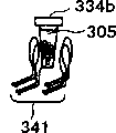
Fig. 10A shows the structure of the reaction apparatus 330 and the distributor 307 used in the above reaction. A capillary tube 308 having an inner diameter of 25um and a length of 21mm was used as the dispenser. By changing the pressure value and the pressure time, the amount of the base solution to be added can be controlled with high accuracy. When the amount of the matrix solution was 0.1. mu.l, the pressure was set to 0.2MPa and the pressure time was 1.1 seconds. The base extension reaction can be controlled by the matching and mismatching of the ends of the primers, and light emission can be observed in the reaction apparatus 330. This means that the sequence corresponding to the primer in the reaction device is located on the target DNA. The photodiode on the measurement device 100 detects the light emission, which is converted into an electrical signal and transmitted by any means of electromagnetic waves, magnetic field changes, or electric field changes. The signal emitted from the measuring device 100 is received at the external antenna 333 and transmitted to the external control unit. As shown in fig. 10A and 10B, by placing an external antenna as close to the measurement apparatus 100 as possible outside the reaction apparatus 330, signal attenuation due to electromagnetic waves, magnetic fields, or electric field changes can be prevented.
(example 10)
In example 9, a method for measuring SNP using chemiluminescence is illustrated. In this example, the present method will be explained with reference to measurement data on the correlation of luciferase concentration. According to the formula shown in example 9, luminescence is generated by a reaction during which luciferin is oxidized in the presence of ATP and luciferase.
(formula 3)
The arrangement of the measuring device shown in FIG. 10 was basically used, except that the measuring device was placed closely just below the outside of the reaction device, and signals were read by the wire.
In particular, AP solution (2X 10)-7M, 0.05. mu.l) was added to a base solution of a buffer (10mM Tris-acetate buffer, pH 7.75) in which luciferin (0.1. mu.g/. mu.l) and luciferase (0.2, 0.5, 1.0, 2.0, 5.0. mu.g/. mu.l) were dissolved. Assuming that the signal accumulation time Tss is 1 second, by observing the change in the signal, the luciferase concentration correlation can be obtained. Fig. 11 shows the results of the measurement. As the luciferase concentration becomes higher, the time constant for the reaction becomes smaller and the peak intensity increases. The maximum change in the output of the photodiode is 1.4mV, and by amplifying this change, analog/digital conversion can be easily achieved.
It has been demonstrated that radio communication can correctly read the identification number using the above-mentioned buffer (10mM Tris-acetate buffer). Since the measuring device is covered with any protective film layer, e.g. SiO2And Si3N4Therefore, even in a solution, the communication function block in the measuring device can operate normally. The communication distance of the measuring device in the buffer solution is 70-80% of that in the air.
(example 11)
Fig. 12 shows in series a process for performing enzyme-linked immunoassay (EIA) according to an embodiment of the present invention. FIGS. 12A, 12B, 12C and 12D show a measuring device, positioned at the photo-electric site, respectivelyAn antigen on the diode, a first antibody on the antigen, and chemiluminescence resulting from an enzyme-linked reaction. Reference is made to the protocol by f.m.ausubel, r.brent, r.b.kingston, d.d.more, j.g.seidman, j.a.smith and k.struhl, john wiley, as a basic protocol&Chemical and bioluminescence are available for measuring oxygen activity in short protocols in Molecular Biology third edition, Sons 1995. In the EIA technique, absorption or luminescence is often used. Luminescence can improve sensitivity, enabling high-precision quantification of antibodies and antigens (Arakawa, h., Maeda, m., and Tsuji,a.,: anal. biochem., 97, p2481979 or Puget, k., Michelson, A.M and Thore, a.,: anal. biochem., 79, p447, 1997). In this example, the use of luminol and H is illustrated2O2The matrix solution of (a) was used in a method of measuring brightness (hv ═ 425nm) by peroxidase. The measuring device 100 was immersed in a solution containing 0.05% (w/v) NaN3The PBS was diluted to 0.2-10. mu.g/ml antigen solution, incubated at 37 ℃ for 2 hours, and coated with antigen 321. The measuring device wasimmersed in a solution containing 1mM EDTA 0.25% (w/v) BSA (bovine serum albumin) and 0.05% (w/v) NaN at room temperature after washing twice with water330 minutes in normal saline and then rinsed three times with water. The primary antibody 320 (the target to be analyzed) obtained from the target sample is diluted to 50. mu.l using the blocking buffer described above. The measurement device 100 was immersed in the solution at room temperature and incubated for 2 hours to allow the first antigen and the antibody to react with each other. The measurement device 100 was rinsed three times with water, then immersed in the blocking buffer for 10 minutes at room temperature, then rinsed three times with water, and then the water was again spin-dried. The measurement device 100 is then incubated for 2 hours or more at room temperature in a diluted solution containing, for example, goat anti-rabbit IgG labeled with peroxidase as a conjugate of the second antibody 322-enzyme 323 (Olsson t., Brunius, g., Carlsson, h.e., and Thore, a.: j.immunol method, 25, p 1271979), and then washed three times with water.
To prepare the matrix solution 324, luminol was dissolved in 0.1N NaOH to obtain a 0.05M solution, which was diluted to 0.01M with 0.2M Tris buffer. The structure shown in fig. 10 can be used for the reaction apparatus and the distributor. The same amount of 0.2M Tris buffer(pH 8.5) and 0.01M H2O2The solution was poured into the reaction apparatus. The measuring device 100 is put into a solution, and the diluted luminol solution is dropped therein. The light emission is detected by the photodiode shown in fig. 8. At this time, by immersing the measuring apparatus 100 in a solution containing the first antigen (the first antigen sample is different) obtained from different samples and measuring, a large number of samples can be measured simultaneously under the same conditions.
(example 12)
The measurement device 100 of the present invention can be used to measure many items to be measured, such as SNPs and different types of proteins at multiple positions on a genome to be measured, simultaneously by placing a plurality of measurement devices 100 in one reaction device as described in example 8. At this time, it is necessary to individually recognize the signals detected by the plurality of measuring devices and read them into the external control unit. In embodiment 1, a method is described in which the identification number 207 of the measurement apparatus 100 is transmitted by the external control unit 206, the measurement apparatus 100 receives the identification number 207, and sensor information is transmitted according to a result of matching with the identification number stored in the measurement apparatus 100. In this embodiment, a flow of signal transmission/reception is described.
Fig. 13A shows a flow of signal transmission/reception when the external control unit 206 transmits the identification number of the target measurement device 100. The identification number of the target measuring device 100 is transmitted from the external control unit 206 to the plurality of measuring devices 100. Each measuring device matches the received signal with an identification number stored in the device. If not, the measurement apparatus 100 stops. If so, sending the sensor information. When a signal is continuously transmitted to the measuring apparatus 100 by the external control unit 206, the transmitted identification number is matched with the stored identification number one bit by one bit. If there is no match at any point, the measurement device 100 will stop the matching process. On the other hand, if the transmitted bits match consecutively with the bits written in the identification number of each measuring device, each measuring device continues to operate. If all bits transmitted match the bits stored in the device, themeasurement device will then transmit the sensor information.
Fig. 13B illustrates a specific stage of the signal transmitted by the external control unit 206 according to the present embodiment, and a method of transmitting the identification number from the measuring apparatus 100 containing the sensor information corresponding to the signal stage to the external control unit 206.
(example 13)
Fig. 14 shows a mechanism of a functional block according to the present embodiment, in which sensor information converted into a digital signal at an analog-to-digital converter (ADC)107 is stored in a memory 190 and transmitted from a measuring device through a signal processing/communication control module. In this case, the sensor information may be only one value at a certain point, or may be a plurality of values at a plurality of time points. The device-specific identification number may be stored at a specific address in memory.
By installing a memory for temporarily storing sensor information, a plurality of data obtained at a plurality of points in time can be stored and transmitted together. At this time, even if the measuring device does not always or frequently communicate with the external control unit 206, the maximum, minimum, and average values in a given period of time may be recorded and transmitted.
(example 14)
Fig. 15A shows the structure of functional blocks of the measuring apparatus 100 according to the embodiment of the present invention. In this example, a shift register is used as the means for recording the identification number. When the number of bits for the identification number is about 10, the circuit can be more easily configured to record and match the identification number than the memory.
Fig. 15B shows a structure having a clock-data separating circuit according to an embodiment of the present invention. At this time, a clock for driving the circuit must be inserted into the circuit block 102 on the measurement apparatus 100. It is preferable that the power consumption of the circuit block 102 on the measuring device 100 is externally supplied by means of electromagnetic waves, magnetic field variation or electric field variation, and the circuit is simplified to save power. To achieve this, a clock may be generated by the external control unit 206 and sent to the measurement device via the carrier device. At circuit block 192, the transmitted clock signal is separated from the data signal and the resulting clock signal is used to drive the individual circuit blocks.
(example 15)
Fig. 16A shows clock signal generation on the measurement device 100. The clock signal is generated by electromagnetic waves, magnetic fields, or electric field variations received by an antenna on the measurement device 100. Thus, an optimal clock can be generated for each measurement device. A clock may be generated that is suitable for circuit blocks on the measurement device.
Fig. 16B is used to illustrate the generation of the clock signal. At this time, some of the clock signals generated on the measurement device 100 are used to drive the sensors. In order to measure the impedance between the microelectrodes described in example 6, an AC or pulse power source had to be installed. In this case, a circuit 193 for generating a clock using an electromagnetic wave, a magnetic field, or a change in an electric field received by the antenna 101 is inserted. The clock generated at the circuit 193 is used to measure the impedance between the microelectrodes. Since the received electromagnetic wave is generally 1MHz or higher, a clock can be obtained by dividing it. Alternatively, the clock may be generated using an oscillator inthe DC power supply described in embodiment 1.
(example 16)
Fig. 17 shows a flow of mounting components for manufacturing the measuring device 100. The use of CMOS for the circuitry mounted on the measuring device allows for high integration and power savings. Therefore, the CMOS mounting process is very critical. Fig. 15 shows an example of a process of assembling a measuring apparatus when the photodiode as described in embodiment 8 is used as a sensor according to an embodiment of the present invention. An element isolation region is formed on a silicon substrate, a photodiode and a MOSFET are mounted, wiring is formed, and a protective film is finally covered.
When the sensor of the FET structure described in embodiment 6 is used, a general-purpose CMOS gate electrode portion of a circuit can be fabricated using a material suitable for probe fixation so that the gate electrode portion can be brought into direct contact with a solution containing a target without a protective film.
The antenna 101 is formed in the process of metallizing the second layer and the third layer (process number 8). If metallization on 2-3 or more layers is required to fabricate the MOSFET circuit, an antenna is formed across these layers in another processing step. No magnetic field lines pass through the conductive layers, such as component mounting and metallization portions of the measurement apparatus 100. Therefore, in order to form the antenna, the thickness of the interlayer insulating film is controlled so that magnetic lines of force can transmit from the measuring apparatus 100 through the film.
(example 17)
Figure 18 shows the structure of a sample/reagent dispenser and an external antenna for measuring many samples simultaneously. In this specification, embodiments having features advantageous for realizing a compact measuring apparatus are described. These embodiments can be readily applied to large systems that can process many samples. By placing the measurement device of the present invention in a reaction device on a standard titer plate 334, where there are also a number of samples and drop reagents, hybridization, affinity binding, and luminescence reactions can be performed. These reactions can be detected by sensors on the measuring device, the sensor information being readable by an external antenna of the respective reaction device.
(example 18)
Figure 19A illustrates a measurement system for measuring samples in a plurality of cuvettes 334 according to an embodiment of the invention. The method for measuring the sample was the same as in example 14. The design of the external antenna is explained below. Fig. 19B shows an example of an antenna design in which a plurality of antennas are closely arranged in the same direction. This design allows the antenna to efficiently communicate with the measurement device 100 at multiple vertical positions in the cuvette. Figure 19C shows a design where the antennas are arranged around the cuvette in different directions. This design may allow the antenna to efficiently communicate with a measurement device 100 placed in solution in a cuvette 334 in multiple orientations. For example, if the external antennas are aligned in three directions and cross each other, the measurement apparatus 100 can efficiently communicate with the external antennas even if the measurement apparatus 100 is oriented in a different direction.
(example 19)
In general, if the measurement device 100 is oriented in different directions, loss occurs in coupling with an external antenna, and the allowable communication distance is also shortened. To avoid this problem, embodiment 19 intends to ensure stability of communication. As shown in fig. 20A and 20B, the bottom of the reaction device 330 is designed to have a flat area so that a plurality of measuring devices are dispersed on the bottom without overlapping when they are put into the reaction device 330. The external antennas are arranged in a plane which is located below and parallel to the bottom of the reaction device. At this time, an oscillator for providing mechanical vibration to the substrate on which the external antenna is formed is mounted. FIG. 20A shows a design in which the oscillator 342 is installed below the reaction apparatus, and FIG. 20B shows a design in which the oscillator 343 is installed on the same horizontal plane as the bottom of the reaction apparatus. By applying vibration to the reaction device, the measurement devices 100 do not overlap, and their chip sides face the bottom of the reaction device, ensuring stable communication between the external antenna and the measurement device.
By designing the element formation region on which the sensor, the circuit, and the antenna of the measurement apparatus 100 are formed to be square and making the ratio between the dimensions of one side of the region and the thickness to be 5 or more (for example, 500 μm × 500 μm, with a thickness of 100 μm or less), the possibility that the side of the chip faces the bottom of the reaction apparatus can be significantly reduced.
The above-mentioned added oscillator also has another desirable effect of accelerating the reaction between the probe fixed on the measuring device and the target. Good agitation and increased rate of molecular motion achieved by vibration allow the reaction to be completed in a shorter time.
(example 20)
The structure of a measuring system according to an aspect of the present invention is explained below. Fig. 21A is an external view of the system, and fig. 21B shows the structure of a reagent dispenser 337, a reaction device (microtiter plate) 340 containing a sample solution and a measuring device, and an integrated external antenna 336 in a shield case 350. In order to ensure information communication and energy transmission between the external control unit and the measuring device, electromagnetic waves, magnetic fields or electric field variations are used. At this time, any measures that can prevent the electromagnetic waves from being diffused to the surrounding area must be taken. To achieve this, a portion that is considered as a source of electromagnetic wave diffusion is put into a shield case. Since in this configuration electromagnetic waves do not leak into the surrounding system area, sufficient energy is supplied from the external antenna to the measuring device 100 in the reaction device, thereby ensuring that the intensity level of electromagnetic waves, magnetic fields, or electric field variations required to establish stable communication can be generated.
According to the embodiments of the present invention described above, measurement can be completed in a short time with the small-sized measurement system and a small number of samples. That is, a simple and fast measuring system can be realized. In addition, the probe can be uniformly fixed on the measuring device, and the probe suitable for different measurements can be easily selected. Multiple target materials can be measured simultaneously in one reaction apparatus. The sensor information and the identification number of the measuring device may be transmitted/received between the measuring device and the external control unit without contacting each other.
The present invention also has the following features.
(1) A biological and chemical sample measuring device, wherein a measuring means is formed on a substrate, the substrate is surface-treated to fix a probe, specific probes are fixed onthe substrate, a sensor for detecting an object captured by the probe is installed, and a structure for determining the presence or amount of the captured object and digitizing the measured value is assembled, the digitized measured value is transmitted to an external unit using an electromagnetic wave, a magnetic field variation or an electric field variation device, an identification number is stored in the measuring means, and the specific measuring means and the type of the probe can be identified by the identification number.
(2) The biological and chemical sample measuring device as described in (1), wherein the probe is any one of an antigen, an antibody, a nucleic acid, and any type of protein, which can be detected as a target.
(3) A biological and chemical sample detection device in which a sensor for detecting temperature, pressure, ion concentration or sugar is mounted on the measuring device, a mechanism for digitizing a signal from the sensor and transmitting the digitized signal to an external unit by means of electromagnetic waves, magnetic field variation or electric field variation is provided, and an identification number by which a specific measuring device and probe type can be identified is stored in the measuring device.
(4) The biological and chemical sample measuring device as described in (1) or (3), wherein functional blocks for transmitting/receiving, detecting and controlling transmission/reception of electromagnetic waves, magnetic fields or electric field variations, which are used for induction, sensor signal processing, identification number recording, and signal transmission and information communication with an external unit, are mounted on the same semiconductor substrate.
(5) The biological and chemical specimen measuring device as described in (1) or (3), wherein an antenna for transmitting/receiving electromagnetic waves is formed on thesame semiconductor substrate as the functional block for induction, sensor signal processing, identification number recording, and signal transmission and information communication with an external unit, controlling transmission/reception of electromagnetic waves, magnetic fields or electric field variations as described in (4), and the distance between two farthest points on the outer shape of the measuring device including the antenna is within 3.0 mm.
(6) The biological and chemical sample measuring device as described in (1) or (3), wherein
(4) The functional block for sensing, sensor signal processing, identification number recording, and signal transmission and information communication with an external unit as described in (1) above, controlling transmission/reception of electromagnetic waves, magnetic fields, or electric field changes consumes energy supplied by external electromagnetic waves, magnetic fields, or electric field changes, and receives it through the antenna as described in (5).
(7) The biological and chemical specimen measuring device as described in (1) or (3), wherein a semiconductor, glass or ceramic substrate is used as a material of the substrate, and the functional block as described in (4) is mounted on the substrate for each measuring device.
(8) The biological and chemical sample measuring device as described in (2), wherein a field effect transistor (hereinafter, abbreviated as FET) is mounted, and presence or absence of specific binding is judged by fixing a probe to a gate of the FET and detecting conductivity between a source and a drain of the transistor based on binding/non-binding between the probe and a target.
(9) A biological and chemical sample measuring device, wherein the presence or absence of specific binding is determined by inserting a separate electrode into a solution, immobilizing a probe on the electrode, recognizing the presence or absence of the captured target or determining the amount thereof based on the binding/non-binding between the probe and the target, observing the change in impedance between the electrodes.
(10) The biological and chemical sample measuring device as set forth in (2), wherein the sensor electrochemically detects the presence or absence of the specific binding when a material specifically binding to the probe and a molecule that dominates the oxidation and reduction processes and selectively binds only to the specific binding site are put in, and transmits the detected data as an electric signal to the external control unit through the information communication means mounted on the chip.
(11) The biological and chemical sample measuring system as set forth in (2), comprising a photodiode as a sensor, which detects the presence or absence of specific binding.
(12) The biological and chemical sample measuring device as described in (1) or (3), comprising a storage area for temporarily storing the digitized measurement signal, the signal data being read out from the storage area and transferred to an external unit.
(13) The biological and chemical sample measuring device as described in (1) or (3), wherein an analog signal measured by a sensor mounted on the semiconductor device is digitized into digital data by a comparator or an analog/digital converter referring to a specific reference signal, the digital data is written into a storage area for temporary storage, and read out from the storage area for transmission to an external unit.
(14) A biological and chemical sample measuring tool kit using the biological and chemical sample measuring device according to (1) or (3), wherein the kit comprises a plurality of biological and chemical measuring devices, a surface of a substrate is processed to fix probes, a plurality of kinds of probes are fixed to each measuring device, and an identification number identifying a specific measuring device and a type of the fixed probe is stored in the measuring device.
(15) The biological and chemical sample measurement tool kit as described in (1), (3) and (14), in which any measurement device on which any antigen, antibody, nucleic acid or any protein is immobilized as a probe and any measurement device on which a sensor for sensing temperature, pressure, ion concentration or sugar is mounted are integrated.
(16) A system for measuring using biological and chemical samples, comprising a plurality of biological and chemical sample measuring devices and a reaction device for putting the measuring devices and samples, wherein the biological and chemical sample measuring devices comprise specific probes, sensors, means for information communication and means for recording identification numbers for identifying the types of the probes, a plurality of probes are fixed, the sensors electrically detect the presence or absence of specific binding when a sample solution is added to the reaction device, and an external control unit performs information communication with the measuring devices through the information communication means using electromagnetic waves, magnetic field variation or electric field variation means.
(17) A biological and chemical sample measuring system, wherein when said biological and chemical sample measuring device (16) is put into a reaction device containing a biological or chemical sample, a target is captured, and a captured signal is detected, and then the measurement signal is transmitted to an external control unit.
(18) A biological and chemical sample measuring system, wherein when a plurality of biological and chemical sample measuring devices as described in (1) or (3) are put into a reaction device containing biological or chemical samples, when a specific first identification number is transmitted from an external unit, the measuring device receives the first identification number and matches it with its own identification number stored internally, and if matching, a sensor on the measuring device whose identification number matches the received identification number transmits a measurement result to an external transmitter/receiver, the external transmitter/receiver transmits a second identification number, the measuring device having the matching identification number transmits the measurement result to the external transmitter/receiver, and then the process is repeated.
(19) A biological and chemical sample measuring system, wherein when a plurality of biological and chemical sample measuring devices as described in (1) or (3) are put into a reaction device containing biological or chemical samples, an external control unit transmits a signal for specifying a specific signal level, the measuring device receives the signal and matches it with a signal level stored internally in a sensor on it, if matching, an identification number having the matched signal level is transmitted to an external transmitter/receiver, or if a plurality of signal levels are detected, the external control unit sequentially transmits signals corresponding to different signal levels, and then the measuring devices having sensor signals associated with these signal levels transmit their own identification numbers to the external control unit.
(20) A biological and chemical sample measuring system, wherein the measuring system performs signal communication between the measuring device described in (1) or (3) and an external control unit which generates a clock signal, and bits of identification numbers are sequentially transmitted on a transmission signal synchronized with the clock signal.
(21) A biological and chemical sample measuring system comprising a reaction device having therein the biological and chemical sample measuring device of (1) or (3) and an external control unit, wherein an antenna for transmission/reception between the measuring device connected to an external control unit and the external control unit is disposed in the same case as that of the measuring device, the case having an electromagnetic shielding function.
(22) A biological and chemical sample measuring system in which an electromagnetic shielding function of a cartridge as described in (21) can attenuate electromagnetic waves emitted from an antenna connected to an external control unit to 1/1000 or less outside the cartridge.
(23) A biological and chemical sample measuring system in which (1) or (3) kinds of said biological and chemical sample measuring devices are put into a plurality of reaction devices, the system performing information communication with a measuring device among said plurality of reaction devices through a same antenna connected to the external control unit or a plurality of antennas corresponding to the respective reaction devices. A biological and chemical sample measuring system using the biological and chemical sample measuring tool kit of (15), comprising a temperature-adjusting heater and a piezoelectric element or an ion concentration-adjusting dispenser, and further comprising a means for monitoring any one of temperature, pH, and ion concentration at regular time intervals using the biological and chemical sample measuring device set in the reaction device of claim 3, and controlling the temperature-adjusting heater and the piezoelectric element or the ion concentration-adjusting dispenser, thereby maintaining the sample at an optimum temperature or an optimum ion concentration level.
In the foregoing specification, the invention has been described with reference to specific embodiments. However, many modifications and variations may be made thereto without departing from the spirit and scope of the invention. Accordingly, the specification and drawings are to be regarded in an illustrative rather than a restrictive sense.