CN1521635A - Device and method for solving deadlock extraction condition in branch target address cache - Google Patents
Device and method for solving deadlock extraction condition in branch target address cache Download PDFInfo
- Publication number
- CN1521635A CN1521635A CNA2004100005482A CN200410000548A CN1521635A CN 1521635 A CN1521635 A CN 1521635A CN A2004100005482 A CNA2004100005482 A CN A2004100005482A CN 200410000548 A CN200410000548 A CN 200410000548A CN 1521635 A CN1521635 A CN 1521635A
- Authority
- CN
- China
- Prior art keywords
- cache
- instruction
- branch
- target address
- address
- Prior art date
- Legal status (The legal status is an assumption and is not a legal conclusion. Google has not performed a legal analysis and makes no representation as to the accuracy of the status listed.)
- Granted
Links
Images


Landscapes
- Advance Control (AREA)
Abstract
本发明是关于一种解决分支目标地址快取中死结提取条件的装置与方法,揭露一种避免微处理器内死结条件的方法,该微处理器包含一推测分支目标地址快取(BTAC),预测一目标地址存在于由指令高速缓存中的一快取线中以响应一提取地址。分支目标地址快取错误地预测分支指令完全存在于快取线中,以至包含分支指令其余部分的下一快取线未被从指令高速缓存中提取。一指令格式器侦测到指令不完全存在于快取线中,停顿下来等待下一快取线。因目标地址并不存在于快取线中,故指令格式器并未收到更多快取线,又因微处理器并未产生推测指令提取,此未命中快取线也没从内存中提取出来。为避免这种死结现象,本发明的装置将分支目标地址快取内的该目标地址无效而重新尝试。
The present invention relates to a device and method for solving deadlock extraction conditions in branch target address cache, and discloses a method for avoiding deadlock conditions in a microprocessor. The microprocessor includes a speculative branch target address cache (BTAC), A target address is predicted to exist in a cache line in the instruction cache in response to a fetch address. The branch target address cache incorrectly predicts that the branch instruction exists entirely in the cache line, so that the next cache line containing the remainder of the branch instruction is not fetched from the instruction cache. An instruction formatter detects that the instruction is not fully present in the cache line and stalls to wait for the next cache line. Since the target address does not exist in the cache line, the instruction formatter does not receive any more cache lines, and since the microprocessor does not generate speculative instruction fetches, the miss cache line is not fetched from memory come out. In order to avoid this deadlock phenomenon, the device of the present invention invalidates the target address in the branch target address cache and tries again.
Description
技术领域technical field
本发明涉及一种微处理器的分支预测(branch prediction),特别是涉及一种利用预测性分支目标地址快取的分支预测。The present invention relates to a branch prediction of a microprocessor, in particular to a branch prediction utilizing predictive branch target address cache.
背景技术Background technique
现代的微处理器都是管线化的微处理器。亦即,在微处理器的不同方块或管线阶段中,可同时操作数个指令。由John L.Hennessy与David A.Patterson在其著作:计算机架构:量化法(Computer Architecture:AQuantitative Approach)(由摩根霍夫曼出版社(加州,旧金山)在1996所出的第二版)中,定义管线为:在执行时,多个指示彼此重叠的实施技术。其提供管线的绝佳描述:Modern microprocessors are pipelined microprocessors. That is, several instructions can operate simultaneously in different blocks or pipeline stages of the microprocessor. By John L. Hennessy and David A. Patterson in Computer Architecture: A Quantitative Approach (Second Edition by Morgan Hoffman Press (San Francisco, CA), 1996), A pipeline is defined as an implementation technique in which multiple instructions overlap each other at execution time. It provides a great description of the pipeline:
管线类似于装配线。在车辆装配线中,有许多步骤,各步骤对车辆的组装做出某些贡献。虽然对于不同的车辆,各步骤的操作平行于其它的步骤。在计算机管线中,管线的各管线完成指令的一部份。类似于装配线,不同步骤完成了平行的不同指令的不同部份。各步骤称为管线阶段或管线部份。这些阶段彼此相连以形成管线,指令从一端进入,经由这些阶段处理,并在另一端中输出,就如同装配线处理车辆般。A pipeline is similar to an assembly line. In a vehicle assembly line, there are many steps, each of which contributes in some way to the assembly of the vehicle. Although for different vehicles, each step operates in parallel to other steps. In a computer pipeline, each pipeline of the pipeline completes a portion of an instruction. Similar to an assembly line, different steps complete different parts of different orders in parallel. Each step is called a pipeline stage or pipeline section. These stages are connected to each other to form a pipeline, with instructions coming in at one end, processed through the stages, and output at the other end, just like an assembly line handles vehicles.
同步微处理器是根据时脉周期而操作。一般而言,在各时脉周期,指令从该微处理器的管线的一阶段前进至另一阶段。在车辆装配线中,如果因为没有车辆要装配使得在线工作员处于闲置,则该线的产量或性能会下降。相似的,如果在一时脉周期中,某一微处理器的管线因为没有指令要操作而处于闲置,通常指此状态为管线气泡,则该微处理器的性能会下降。Synchronous microprocessors operate according to clock cycles. In general, an instruction advances from one stage of the microprocessor's pipeline to another at each clock cycle. In a vehicle assembly line, if line workers are idle because there are no vehicles to assemble, the line's output or performance will drop. Similarly, if the pipeline of a microprocessor is idle during a clock cycle because there are no instructions to operate on, this state is usually referred to as a pipeline bubble, and the performance of the microprocessor will be degraded.
造成管线气泡的可能原因之一是分支指令。当处理分支指令时,处理器必需决定该分支指令的目的地址并开始在该目标地址处而非在该分支指令后的下一地址处撷取指令。甚至,如果该分支指令是一状况分支指令(亦即,必需根据一特定状况是否存在而决定该分支是否要执行),除了决定该目标地址外,该处理器更必需决定该分支指令是否要执行。因为最后决定该目标地址及/或分支结果(亦即分支是否要执行)的该管线阶段通常处于指令撷取阶段的下方,可能会产生气泡。One of the possible causes of pipeline bubbles is branch instructions. When processing a branch instruction, the processor must determine the target address of the branch instruction and start fetching instructions at the target address rather than at the next address after the branch instruction. Even, if the branch instruction is a conditional branch instruction (i.e., it is necessary to decide whether the branch is to be executed based on whether a specific condition exists or not), in addition to determining the target address, the processor must also determine whether the branch instruction is to be executed . Because the pipeline stage that finally determines the target address and/or branch outcome (ie, whether the branch is to be taken) is usually below the instruction fetch stage, bubbles may occur.
为解决此问题,现代微处理器一般应用分支预测机制以在管线的早期预测目标地址与分支结果。分支预测机制的一例是分支目标地址快取(branch target address cache,BTAC),其平行于从该微处理器的一指令快取撷取指令而预测该分支结果与目标地址。当微处理器执行分支指令且最后决定要执行该分支与决定其目标地址时,该分支指令的地址与其目标地址是写入至该BTAC内。下次从该指令快取撷取该分支指令时,该分支指令地址会命中于该BTAC内且该BTAC可在管线早期输出该分支指令目标地址。To solve this problem, modern microprocessors generally employ branch prediction mechanisms to predict target addresses and branch outcomes early in the pipeline. One example of a branch prediction mechanism is a branch target address cache (BTAC), which predicts the branch outcome and target address in parallel to fetching instructions from an instruction cache of the microprocessor. When the microprocessor executes a branch instruction and finally decides to execute the branch and determines its target address, the address of the branch instruction and its target address are written into the BTAC. The next time the branch instruction is fetched from the instruction cache, the branch instruction address will hit in the BTAC and the BTAC can output the branch instruction target address early in the pipeline.
有效的BTAC可排除或减少要等待分支指令决定的气泡数量,以改善处理器性能。然而,当该BTAC预测错误时,错误撷取指令的管线的部份必需被放弃,以及必需撷取正确指令,当指令放弃与撷取发生时,会在管线内造成气泡。当微处理器的管线更深时,BTAC的有效性更会是影响性能的关键处。An effective BTAC improves processor performance by removing or reducing the number of bubbles waiting for branch instruction decisions. However, when the BTAC mispredicts, the portion of the pipeline that fetched the wrong instruction must be aborted, and the correct instruction must be fetched, causing bubbles in the pipeline when instruction abandonment and fetching occur. When the pipeline of the microprocessor is deeper, the effectiveness of BTAC will be the key point affecting the performance.
BTAC的有效性主要是BTAC的命中率的作用。影响BTAC命中率的因素之一是其所储存目标地址的不同分支指令数量。储存更多的分支指令目标地址,BTAC更有效。然而,在微处理器芯片面积总是有限,因而要尽可能令既定功能方块(比如BTAC)的面积变小。影响BTAC的实际面积之一因素是将目标地址与相关信息储存于BTAC内的储存晶胞的大小。特别是,单埠晶胞的面积小于多埠晶胞的面积。由单埠晶胞组成的BTAC在一既定时脉周期内只能读或写,无法同时进行读写,但由多埠晶胞组成的BTAC可在一既定时脉周期内同时进行读写。然而,多埠BTAC的面积大于单埠BTAC。这意味着,假设给定BTAC的被允许实际面积,多端口BTAC可储存的目标地址数量必需小于单端口BTAC可储存的目标地址数量,因而会降低BTAC的有效性。因此,由此观点来看,单埠BTAC是较佳的。The effectiveness of the BTAC is primarily a function of the hit rate of the BTAC. One of the factors affecting the hit rate of a BTAC is the number of different branch instructions for the target address it stores. Store more branch instruction target addresses, BTAC is more efficient. However, the chip area of a microprocessor is always limited, so the area of a given functional block (such as BTAC) should be reduced as much as possible. One of the factors that affects the actual area of a BTAC is the size of the memory cell that stores the target address and related information within the BTAC. In particular, the area of a single-port unit cell is smaller than the area of a multi-port unit cell. A BTAC composed of a single-port unit cell can only read or write within a given clock cycle, and cannot read and write at the same time, but a BTAC composed of multi-port unit cells can simultaneously read and write within a given clock cycle. However, the area of a multi-port BTAC is larger than that of a single-port BTAC. This means that, given the allowed physical area of the BTAC, the number of target addresses that a multi-port BTAC can store must be smaller than that of a single-port BTAC, thus reducing the effectiveness of the BTAC. Therefore, from this point of view, a single-port BTAC is preferable.
然而,由于单埠BTAC在一既定时脉周期内只能读或写,无法同时进行读写,此事实会因为伪性未命中(false miss)而降低BTAC有效性。在BTAC需要被读取的周期中,当单埠BTAC正被写入,比如利用新目标地址来更新BTAC或要使某一目标地址无效时,会发生伪性未命中。在此情况下,BTAC必需对该读取产生未命中,因为其无法供给可能已存在于BTAC内的该目标地址,因为该BTAC正被写入。However, since a single-port BTAC can only read or write in a given clock cycle, and cannot read and write simultaneously, this fact reduces the effectiveness of the BTAC due to false misses. Spurious misses can occur when the single-port BTAC is being written to, such as updating the BTAC with a new target address or invalidating a target address, during the cycle that the BTAC needs to be read. In this case, the BTAC must miss the read because it cannot supply the target address, which may already exist in the BTAC, since the BTAC is being written to.
因而,需要一种能降低单埠BTAC内的伪性未命中的方法与装置。Therefore, there is a need for a method and apparatus for reducing spurious misses in a single-port BTAC.
可能会降低BTAC有效性的另一现象是BTAC会多次储存分支指令的目标地址。此现象可能发生于多向指令集联合(multi-wayset-associative)BTAC内。因为BTAC空间有限,多余的目标地址储存会降低BTAC有效性,因为多余BTAC项目可储存另一分支指令的目标地址。管线愈长,亦即阶段数愈大,多余目标地址愈可能会存于BTAC内。Another phenomenon that may reduce the effectiveness of BTAC is that BTAC stores the target address of a branch instruction multiple times. This phenomenon may occur in a multi-wayset-associative BTAC. Because BTAC space is limited, redundant target address storage reduces BTAC effectiveness because redundant BTAC entries can store the target address of another branch instruction. The longer the pipeline, that is, the larger the number of stages, the more likely redundant target addresses will be stored in the BTAC.
同一分支指令在BTAC内被多次快取的最常见的情况是在码的紧凑循环内。第一次执行分支指令且其目标地址是写入至该BTAC,比如写至2向,因为2向是最久未用。然而,在目标地址写入至BTAC之前,分支指令再次出现,亦即该BTAC查调未命中的该指令快取撷取地址,因为该目标地址尚未写入至该BTAC内。接着,会将目标地址第二次写入至该BTAC。如果在该指令集内插入不同分支指令的BTAC读取造成2向不再是最久未用,则另一向,比如1向,会被选择成第二次写入该目标地址。现在,同一分支指令的目标地址二次存在于该BTAC内。这是一种BTAC空间浪费且会降低BTAC的有效性,因为第二次写入很可能会覆盖另一分支指令的有效目标地址。The most common case where the same branch instruction is cached multiple times within a BTAC is within a tight loop of code. The branch instruction is executed for the first time and its target address is written to the BTAC, for example, written to 2-way, because 2-way is the longest unused. However, before the target address is written into the BTAC, the branch instruction occurs again, ie, the BTAC poll misses the instruction cache fetch address because the target address has not been written into the BTAC. Next, the target address is written to the BTAC a second time. If a BTAC read of a different branch instruction inserted within the instruction set causes 2-way to no longer be the least recently used, then another way, such as 1-way, would be selected for the second write to the target address. Now, the target address of the same branch instruction exists twice in the BTAC. This is a waste of BTAC space and reduces the effectiveness of BTAC, since the second write will likely overwrite the effective target address of another branch instruction.
因此,需要一种能避免同一分支指令的目标地址的多余快取所造成的有用BTAC空间浪费的方法与装置。Therefore, there is a need for a method and apparatus for avoiding waste of useful BTAC space caused by redundant caching of the target address of the same branch instruction.
甚至,相关于BTAC预测性的某些情况的组合会造成微处理内的死结。BTAC的分支预测的组合,跨越指令快取边界线的分支指令,以及处理器总线会交易预测性指令撷取的事实,会造成错误情况,导致某些情况下的死结。Furthermore, certain combinations of conditions related to BTAC predictability can create deadlocks within the microprocessor. The combination of BTAC's branch prediction, branch instructions that cross instruction cache boundaries, and the fact that the processor bus trades predictive instruction fetches can create error conditions that lead to deadlocks in some cases.
因而,需要一种能避免应用预测性BTAC的微处理器内的死结情况的方法与装置。Accordingly, what is needed is a method and apparatus for avoiding deadlock conditions in microprocessors employing predictive BTACs.
发明内容Contents of the invention
本发明的目的在于,提供一种新的解决分支目标地址快取中死结提取条件的装置与方法,所要解决的技术问题是使其能够使得采用此一分支目标地址快取预测一分支指令的目标地址可以跨越快取线的边界的微处理器提供正确的程序设计操作。The object of the present invention is to provide a new device and method for solving the deadlock extraction condition in the branch target address cache, the technical problem to be solved is to make it possible to use this branch target address cache to predict the target of a branch instruction Microprocessors whose addresses can cross cache line boundaries provide correct programming operations.
本发明的目的及解决其技术问题是采用以下技术方案来实现的。依据本发明提出的一种微处理器内具有一推测分支目标地址快取(BTAC)的一死结避免装置,该装置包括:一第一信号,用以指示一指令高速缓存中的一提取地址未命中,其中该提取地址是由该分支目标地址快取所提供的一推测分支指令目标地址;一第二信号,用以指示该分支指令跨越两条快取线;一第三信号,用以指示该分支目标地址快取预测该分支指令并未跨越两条快取线,其中该两条快取线之一第二快取线因此而并未提取;以及控制逻辑电路,耦合至该第一、第二及第三信号,以响应于该第一、第二及第三信号的真值指示而将该分支目标地址快取内的该目标地址无效。The purpose of the present invention and the solution to its technical problems are achieved by adopting the following technical solutions. A deadlock avoidance device with a speculative branch target address cache (BTAC) in a microprocessor proposed according to the present invention, the device includes: a first signal for indicating that a fetch address in an instruction cache is not hit, wherein the fetch address is a speculative branch instruction target address provided by the branch target address cache; a second signal is used to indicate that the branch instruction crosses two cache lines; a third signal is used to indicate The branch target address cache predicts that the branch instruction does not cross two cache lines, wherein a second one of the two cache lines is therefore not fetched; and control logic coupled to the first, second and third signals for invalidating the target address in the branch target address cache in response to true values of the first, second and third signals indicating.
本发明的目的及解决其技术问题还可采用以下技术措施进一步实现。The purpose of the present invention and its technical problems can also be further realized by adopting the following technical measures.
前述的装置,其中所述的控制逻辑电路更组态为在将该分支目标地址快取内的该目标地址无效之后会使该微处理器分支至该分支指令。The aforementioned apparatus, wherein the control logic circuit is further configured to cause the microprocessor to branch to the branch instruction after invalidating the target address in the branch target address cache.
前述的装置,其中所述的一指令格式器藉由译码该两条快取线之一第一快取线来决定该分支指令是否跨越两条快取线。In the aforementioned device, the instruction formatter determines whether the branch instruction crosses two cache lines by decoding a first cache line of the two cache lines.
前述的装置,其中所述的装置,其中所述的指令高速缓存提供该两条快取线的该第一快取线。The aforementioned device, wherein the device, wherein the instruction cache provides the first cache line of the two cache lines.
前述的装置,其中所述的分支指令目标地址是推测的是因该目标地址仅是预测的并不保证一定是该分支指令一个正确的目标地址。In the aforementioned device, the target address of the branch instruction is speculated because the target address is only predicted and does not guarantee to be a correct target address of the branch instruction.
前述的装置,其中所述的装置,其中所述的分支指令目标地址是推测的是因该目标地址也许是另一分支指令的一目标地址。The aforementioned apparatus, wherein the apparatus, wherein the target address of the branch instruction is guessed because the target address may be a target address of another branch instruction.
前述的装置,其中所述的装置,其中所述的分支指令目标地址是推测的是因该分支指令也许现在不存在于该两条快取线中。The aforementioned apparatus, wherein said apparatus, wherein said branch instruction target address is speculative because the branch instruction may not currently exist in the two cache lines.
前述的装置,其中所述的装置,其中所述的两条快取线之一第二快取线并未提取是包含该两条快取线之一第二快取线并未从与耦接至该微处理器的一内存中提取。The aforementioned device, wherein the device, wherein the second cache line of the two cache lines does not fetch includes that the second cache line of the two cache lines is not coupled from the to a memory of the microprocessor.
本发明的目的及解决其技术问题还采用以下的技术方案来实现。依据本发明提出的一种避免死结条件的管线微处理器,其包括:一分支目标地址快取,用以提供一分支指令之一推测目标地址以响应一指令快取提取地址;以及一控制逻辑电路,耦合至该分支目标地址快取,以响应于一侦测条件而将该分支目标地址快取内的该推测目标地址无效,其中:在该指令高速缓存响应该提取地址而提供一第一快取线之后,该推测目标地址产生未命中,其中该第一快取线仅含有一部份的该分支指令;该分支目标地址快取错误地预测该分支指令完全存在于该第一快取线中而导致含有该分支指令另一部份的一第二快取线并未从该指令高速缓存中提取。The purpose of the present invention and the solution to its technical problems are also achieved by the following technical solutions. A pipeline microprocessor for avoiding a deadlock condition according to the present invention includes: a branch target address cache for providing a speculative target address of a branch instruction in response to an instruction cache fetch address; and a control logic circuitry, coupled to the branch target address cache, to invalidate the speculative target address within the branch target address cache in response to a detected condition, wherein: the instruction cache provides a first The speculative target address misses after a cache line in which the first cache line contains only a portion of the branch instruction; the branch target address cache incorrectly predicts that the branch instruction exists entirely in the first cache A second cache line containing another portion of the branch instruction is not fetched from the instruction cache.
本发明的目的及解决其技术问题还可采用以下技术措施进一步实现。The purpose of the present invention and its technical problems can also be further realized by adopting the following technical measures.
前述的微处理器,其中所述的微处理器,其中所述的控制逻辑电路更组态为在响应该侦测条件而将该分支目标地址快取内的该推测目标地址无效之后会使该微处理器分支回该提取地址。The foregoing microprocessor, wherein the microprocessor, wherein the control logic circuit is further configured to invalidate the speculative target address in the branch target address cache in response to the detected condition The microprocessor branches back to the fetched address.
前述的微处理器,其中所述的微处理器,其更包括:一指令提取器,耦合至该控制逻辑电路,将未命中的该些快取线自耦接至该微处理器的一内存中提取,其中该指令提取器是组态为不会由该分支目标地址快取所提供的推测目标地址中提取该些未命中的快取线。The aforementioned microprocessor, wherein said microprocessor further includes: an instruction fetcher, coupled to the control logic circuit, and coupling the cache lines of misses to a memory of the microprocessor fetch, wherein the instruction fetcher is configured not to fetch the miss cachelines from speculative target addresses provided by the branch target address cache.
前述的微处理器,其中所述的微处理器,其更包括:一指令格式器,耦合至该控制逻辑电路,藉由译码该第一快取线来产生一信号至该控制逻辑电路以指示该分支指令是不完全存在于该第一快取线中。The aforementioned microprocessor, wherein the microprocessor further includes: an instruction formatter, coupled to the control logic circuit, generates a signal to the control logic circuit by decoding the first cache line Indicates that the branch instruction is not fully present in the first cache line.
前述的微处理器,其中所述的微处理器,其更包括:一指令缓冲器,耦合至该指令高速缓存,用以自该指令高速缓存接收该第一快取线并在该指令格式器译码该第一快取线时储存该第一快取线。The aforementioned microprocessor, wherein said microprocessor further includes: an instruction buffer coupled to the instruction cache for receiving the first cache line from the instruction cache and storing the first cache line in the instruction formatter The first cache line is stored when decoding the first cache line.
前述的微处理器,其中所述的微处理器,其更包括:执行逻辑电路,耦合至该控制逻辑电路,用以侦测并更正该分支目标地址快取的错误预测,其中该执行逻辑电路并不侦测因为该指令格式器等待该第二快取线提取的停顿而造成该分支目标地址快取错误地预测该分支指令完全存在于该第一快取线中。The foregoing microprocessor, wherein the microprocessor further includes: an execution logic circuit coupled to the control logic circuit for detecting and correcting misprediction of the branch target address cache, wherein the execution logic circuit It does not detect that the branch target address cache incorrectly predicts that the branch instruction exists entirely in the first cache line because the instruction formatter waits for a stall in the second cache line to be fetched.
本发明的目的及解决其技术问题还采用以下的技术方案来实现。依据本发明提出的一种避免微处理器内死结条件的方法,该微处理器包含有一指令高速缓存及一推测分支目标地址快取,该方法包括以下步骤:产生一推测目标地址部分存在于由该指令高速缓存中的一第一快取线以响应使用于该分支目标地址快取的一第一提取地址;提供该目标地址作为一第二提取地址给该指令高速缓存而没有提取该第一快取线之后的下一快取线,以响应该部分存在于由该指令高速缓存中的一第一快取线以响应完全存在于该第一快取线中的该分支目标地址快取预测的该分支指令;判断该分支目标地址快取错误地预测该分支指令完全存在于该第一快取线中;侦测一未命中于该指令高速缓存中的该目标地址;以及将该分支目标地址快取内的该目标地址无效以响应于该判断与该侦测。The purpose of the present invention and the solution to its technical problems are also achieved by the following technical solutions. According to a method for avoiding deadlock conditions in a microprocessor provided by the present invention, the microprocessor includes an instruction cache and a speculative branch target address cache, and the method includes the following steps: generating a speculative target address part that exists in the a first cache line in the instruction cache in response to a first fetch address used for the branch target address cache; providing the target address as a second fetch address to the instruction cache without fetching the first the next cache line after the cache line in response to the branch target address cache prediction that is partially present in the instruction cache in response to the branch target address being fully present in the first cache line determining the branch target address cache incorrectly predicting that the branch instruction exists entirely in the first cache line; detecting a miss at the target address in the instruction cache; and The target address in the address cache is invalidated in response to the determination and the detection.
本发明的目的及解决其技术问题还可采用以下技术措施进一步实现。The purpose of the present invention and its technical problems can also be further realized by adopting the following technical measures.
前述的方法,其中所述的方法,其更包括:在该无效动作后,将该微处理器分支至一分支指令的地址。The foregoing method, wherein the method further includes: after the invalid action, branching the microprocessor to an address of a branch instruction.
前述的方法,其中所述的方法,其中将该微处理器分支至该分支指令的地址是包含提供该第一提取地址给该指令高速缓存作为下一个提取地址。The aforementioned method, wherein the method wherein branching the microprocessor to the address of the branch instruction includes providing the first fetch address to the instruction cache as a next fetch address.
前述的方法,其中所述的方法,其中将该微处理器分支至该分支指令的地址是包含分派该分支指令的该地址给该微处理器中的一指令指针缓存器。The aforementioned method, wherein the method wherein branching the microprocessor to the address of the branch instruction includes assigning the address of the branch instruction to an instruction pointer register in the microprocessor.
本发明的目的及解决其技术问题还采用以下的技术方案来实现。依据本发明提出的一传输媒介内的计算机数据信号,其包括:计算机可读式程序代码,提供给一微处理器,该程序代码包括:第一程序代码,提供一分支目标地址快取(BTAC),及提供一分支指令之一推测目标地址以响应于一指令快取提取地址;以及第二程序代码,提供给耦接至一分支目标地址快取(BTAC)的控制逻辑电路,将该分支目标地址快取中的该推测目标地址无效以响应一侦测条件,其中:在该指令高速缓存提供一第一快取线以响应该提取地址后,该推测目标地址未命中该指令高速缓存,其中该第一快取线仅包含一第一部分的该分支指令;以及该分支目标地址快取错误地预测该分支指令完全存在于该第一快取线中,以至于包含该分支指令的一第二部分的一第二快取线未被从该指令高速缓存中提取。The purpose of the present invention and the solution to its technical problems are also achieved by the following technical solutions. According to the computer data signal in a transmission medium proposed by the present invention, it includes: computer-readable program code, which is provided to a microprocessor, and the program code includes: first program code, which provides a branch target address cache (BTAC ), and providing a speculative target address of a branch instruction in response to an instruction cache fetch address; and second program code, provided to control logic coupled to a branch target address cache (BTAC), to branch the speculative target address in the target address cache is invalidated in response to a detected condition, wherein: the speculative target address misses the instruction cache after the instruction cache provides a first cache line in response to the fetch address, wherein the first cache line contains only a first portion of the branch instruction; and the branch target address cache incorrectly predicts that the branch instruction exists entirely in the first cache line such that a first portion of the branch instruction contains Two portions of a second cache line are not fetched from the instruction cache.
本发明与现有技术相比具有明显的优点和有益效果。由以上技术方案可知,为了达到前述发明目的,本发明的主要技术内容如下:Compared with the prior art, the present invention has obvious advantages and beneficial effects. As can be seen from the above technical solutions, in order to achieve the aforementioned object of the invention, the main technical contents of the present invention are as follows:
本发明提供一种解决微处理器中分支目标地址快取(BTAC)死结提取条件的装置与方法,此一分支目标地址快取预测一分支指令的目标地址也许会跨越快取线的边界。在一观点中,本发明提供一微处理器内具有一推测分支目标地址快取(BTAC)的一死结避免装置,该装置包括:一第一信号,用以指示一指令高速缓存中的一提取地址未命中,其中该提取地址是由该分支目标地址快取所提供的一推测分支指令目标地址。该装置又包括一第二信号,用以指示该分支指令跨越两条快取线。该装置还包括一第三信号,用以指示该分支目标地址快取预测该分支指令并未跨越两条快取线,其中该两条快取线的一第二快取线因此而并未提取。该装置更包括一控制逻辑电路,耦合至该第一、第二及第三信号,以响应于该第一、第二及第三信号的真值指示而将该分支目标地址快取内的该目标地址无效。The present invention provides an apparatus and method for solving the deadlock extraction condition of branch target address cache (BTAC) in a microprocessor. The branch target address cache predicts that the target address of a branch instruction may cross the cache line boundary. In one aspect, the present invention provides a deadlock avoidance apparatus having a speculative branch target address cache (BTAC) in a microprocessor, the apparatus comprising: a first signal indicating a fetch in an instruction cache An address miss where the fetch address is a speculative branch instruction target address provided by the branch target address cache. The device further includes a second signal for instructing the branch instruction to cross two cache lines. The apparatus also includes a third signal for indicating that the branch target address cache predicts that the branch instruction does not cross two cache lines, wherein a second cache line of the two cache lines is therefore not fetched . The device further includes a control logic circuit, coupled to the first, second and third signals, for instructing the branch target address in the branch target address cache in response to true indications of the first, second and third signals. Invalid destination address.
在另一观点中,本发明提供一种避免死结条件的管线微处理器,该微处理器包括一分支目标地址快取,用以提供一分支指令的一推测目标地址以响应一指令快取提取地址,该微处理器也包括一控制逻辑电路,耦合至该分支目标地址快取,以响应于一侦测条件而将该分支目标地址快取内的该推测目标地址无效,其中该侦测条件为在该指令高速缓存响应该提取地址而提供一第一快取线之后,该推测目标地址产生未命中,其中该第一快取线仅含有一部份的该分支指令,同时该分支目标地址快取错误地预测该分支指令完全存在于该第一快取线中而导致含有该分支指令另一部份的一第二快取线并未从该指令高速缓存中提取。In another aspect, the present invention provides a pipelined microprocessor for avoiding deadlock conditions, the microprocessor including a branch target address cache for providing a speculative target address of a branch instruction in response to an instruction cache fetch address, the microprocessor also includes a control logic circuit coupled to the branch target address cache to invalidate the speculative target address in the branch target address cache in response to a detected condition, wherein the detected condition The speculative target address generates a miss after the instruction cache provides a first cache line in response to the fetch address, wherein the first cache line contains only a portion of the branch instruction while the branch target address The cache incorrectly predicts that the branch instruction exists entirely in the first cache line, causing a second cache line containing another portion of the branch instruction to not be fetched from the instruction cache.
在又一观点中,本发明提供一种避免微处理器内死结条件的方法,该微处理器包含有一指令高速缓存及一推测分支目标地址快取。该方法是包括产生一推测目标地址部分存在于由该指令高速缓存中的一第一快取线以响应使用于该分支目标地址快取的一第一提取地址,该方法且包括提供该目标地址作为一第二提取地址给该指令高速缓存而没有提取该第一快取线之后的下一快取线,以响应该部分存在于由该指令高速缓存中的一第一快取线以响应完全存在于该第一快取线中的该分支目标地址快取预测的该分支指令,该方法又包括判断该分支目标地址快取错误地预测该分支指令完全存在于该第一快取线中,该方法另包括侦测一未命中于该指令高速缓存中的该目标地址,该方法还包括将该分支目标地址快取内的该目标地址无效以响应于该判断与该侦测。In yet another aspect, the present invention provides a method for avoiding deadlock conditions in a microprocessor including an instruction cache and a speculative branch target address cache. The method includes generating a speculative target address portion present in a first cache line in the instruction cache in response to a first fetch address used for the branch target address cache, and includes providing the target address as a second fetch address to the instruction cache without fetching the next cache line after the first cache line in response to the partial presence of a first cache line in the instruction cache in response to a complete The branch target address cache that exists in the first cache line predicts the branch instruction, the method further includes determining that the branch target address cache incorrectly predicts that the branch instruction exists entirely in the first cache line, The method further includes detecting a miss on the target address in the instruction cache, and the method further includes invalidating the target address in the branch target address cache in response to the determining and the detecting.
在另一观点中,本发明提供一种实施于一传输媒介内的计算机数据信号,包括计算机可读式程序代码,提供给一微处理器,该程序代码包括第一程序代码,提供一分支目标地址快取(BTAC),及提供一分支指令的一推测目标地址以响应于一指令快取提取地址,该程序代码也包括第二程序代码,提供给耦接至一分支目标地址快取(BTAC)的控制逻辑电路,将该分支目标地址快取中的该推测目标地址无效以响应一侦测条件,其中在该指令高速缓存提供一第一快取线以响应该提取地址后,该推测目标地址未命中该指令高速缓存,其中该第一快取线仅包含一第一部分的该分支指令,以及该分支目标地址快取错误地预测该分支指令完全存在于该第一快取线中,以至于包含该分支指令的一第二部分的一第二快取线未被从该指令高速缓存中提取。In another aspect, the present invention provides a computer data signal embodied in a transmission medium, including computer readable program code provided to a microprocessor, the program code including first program code providing a branch target address cache (BTAC), and providing a speculative target address of a branch instruction in response to an instruction cache fetching address, the program code also includes second program code coupled to a branch target address cache (BTAC) ) to invalidate the speculative target address in the branch target address cache in response to a detected condition, wherein after the instruction cache provides a first cache line in response to the fetch address, the speculative target an address misses the instruction cache, wherein the first cache line contains only a first portion of the branch instruction, and the branch target address cache incorrectly predicts that the branch instruction exists entirely in the first cache line, to A second cache line containing a second portion of the branch instruction is not fetched from the instruction cache.
在另一观点中,本发明提供一种实施于一传输媒介内的计算机数据信号,包括计算机可读式程序代码,提供给一具有一推测分支目标地址快取(BTAC)的一死结避免装置的一微处理器,该程序代码包括第一程序代码,提供一第一信号用以指示一指令高速缓存中的一提取地址未命中,其中该提取地址是由该分支目标地址快取所提供的一推测分支指令目标地址,该程序代码也包括第二程序代码,提供一第二信号,用以指示该分支指令跨越两条快取线,该程序代码又包括第三程序代码,提供一第三信号,用以指示该分支目标地址快取预测该分支指令并未跨越两条快取线,其中该两条快取线的一第二快取线因此而并未提取,该程序代码还包括第四程序代码提供给一控制逻辑电路,耦合至该第一、第二及第三信号,以响应于该第一、第二及第三信号的真值指示而将该分支目标地址快取内的该目标地址无效。In another aspect, the present invention provides a computer data signal embodied in a transmission medium, including computer readable program code, provided to a deadlock avoidance device having a speculative branch target address cache (BTAC). A microprocessor, the program code includes first program code for providing a first signal indicating a miss in a fetch address in an instruction cache, wherein the fetch address is a fetch provided by the branch target address cache Inferring the target address of the branch instruction, the program code also includes a second program code that provides a second signal to indicate that the branch instruction crosses two cache lines, and the program code includes a third program code that provides a third signal , used to indicate that the branch target address cache predicts that the branch instruction does not cross two cache lines, wherein a second cache line of the two cache lines is therefore not fetched, and the program code also includes a fourth Program code is provided to a control logic circuit, coupled to the first, second and third signals, for instructing the branch target address in the branch target address cache in response to true indications of the first, second and third signals. Invalid destination address.
经由上述可知,本发明揭露一种避免微处理器内死结条件的方法,该微处理器包含有一推测分支目标地址快取(BTAC),预测一目标地址存在于由该指令高速缓存中的一快取线中以响应一提取地址。该分支目标地址快取错误地预测该分支指令完全存在于该快取线中,以至于包含该分支指令的其余部分的下一快取线未被从该指令高速缓存中提取。一指令格式器侦测到该指令不完全存在于该快取线中,而停顿下来等待下一快取线。然而,因为该目标地址并不存在于该快取线中,所以该指令格式器并未收到更多的快取线,同时又因为该微处理器并未产生推测指令提取,此未命中的快取线也没有从内存中提取出来。为了避免这种死结现象,本发明的装置将该分支目标地址快取内的该目标地址无效而重新尝试。As can be seen from the foregoing, the present invention discloses a method of avoiding deadlock conditions in a microprocessor that includes a speculative branch target address cache (BTAC) that predicts that a target address exists in a cache stored in the instruction cache. Fetch the line in response to a fetch address. The branch target address cache incorrectly predicts that the branch instruction exists entirely in the cache line so that the next cache line containing the remainder of the branch instruction is not fetched from the instruction cache. An instruction formatter detects that the instruction is not fully present in the cache line and stalls for the next cache line. However, because the target address does not exist in the cache line, the instruction formatter receives no more cache lines, and because the microprocessor does not generate speculative instruction fetches, the miss The cache line is also not fetched from memory. In order to avoid this deadlock phenomenon, the apparatus of the present invention invalidates the target address in the branch target address cache and tries again.
借由上述技术方案,本发明解决分支目标地址快取中死结提取条件的装置与方法至少具有下列优点:本发明能够使得采用此一分支目标地址快取预测一分支指令的目标地址可以跨越快取线的边界的微处理器提供正确的程序设计操作。By means of the above-mentioned technical solution, the device and method for solving the deadlock extraction condition in the branch target address cache of the present invention have at least the following advantages: the present invention can make use of this branch target address cache to predict that the target address of a branch instruction can span the cache Line-of-the-line microprocessors provide correct programming operations.
综上所述,本发明具有上述优点及实用价值,并在同类产品及方法中未见有类似的结构设计及方法公开发表或使用而确属创新,其不论在产品结构、方法或功能上皆有较大的改进,在技术上有较大的进步,并产生了好用及实用的效果,从而更加适于实用,而具有产业的广泛利用价值,诚为一新颖、进步、实用的新设计。In summary, the present invention has the above-mentioned advantages and practical value, and there is no similar structural design and method publicly published or used in similar products and methods, so it is indeed an innovation, no matter in product structure, method or function. It has been greatly improved, has made great progress in technology, and has produced easy-to-use and practical effects, so it is more suitable for practical use, and has wide application value in the industry. It is a novel, progressive and practical new design. .
上述说明仅是本发明技术方案的概述,为了能够更清楚了解本发明的技术手段,并可依照说明书的内容予以实施,以下以本发明的较佳实施例并配合附图详细说明如后。The above description is only an overview of the technical solutions of the present invention. In order to understand the technical means of the present invention more clearly and implement them according to the contents of the description, the preferred embodiments of the present invention and accompanying drawings are described in detail below.
附图说明Description of drawings
图1显示根据本发明的微处理器的方块图。Fig. 1 shows a block diagram of a microprocessor according to the present invention.
图2显示根据本发明的图1的微处理器的部份详细方块图。FIG. 2 shows a partially detailed block diagram of the microprocessor of FIG. 1 in accordance with the present invention.
图3显示根据本发明的图1的BTAC的部份详细方块图。FIG. 3 shows a partially detailed block diagram of the BTAC of FIG. 1 according to the present invention.
图4显示根据本发明的图3的目标地址数组项目内容的方块图。FIG. 4 shows a block diagram of the contents of the target address array items of FIG. 3 according to the present invention.
图5显示根据本发明的图3的卷标数组项目内容的方块图。FIG. 5 shows a block diagram of the contents of the tag array item of FIG. 3 according to the present invention.
图6显示根据本发明的图3的计数器数组项目内容的方块图。FIG. 6 shows a block diagram of the contents of the counter array entries of FIG. 3 according to the present invention.
图7显示根据本发明的图1的BTAC写入要求内容的方块图。FIG. 7 shows a block diagram of the BTAC write request content of FIG. 1 according to the present invention.
图8显示根据本发明的图3的BTAC写入队列的方块图。FIG. 8 shows a block diagram of the BTAC write queue of FIG. 3 according to the present invention.
图9显示根据本发明的图1的BTAC写入队列的操作流程图。FIG. 9 shows a flowchart of the operation of the BTAC write queue of FIG. 1 according to the present invention.
图10显示根据本发明的图1的该微处理器内的该BTAC的多余目标地址无效逻辑电路的方块图。10 shows a block diagram of redundant target address invalidation logic circuitry of the BTAC within the microprocessor of FIG. 1 according to the present invention.
图11显示根据本发明的图10的多余目标地址装置的操作流程图。FIG. 11 is a flowchart showing the operation of the redundant target address device of FIG. 10 according to the present invention.
图12显示根据本发明的图1的该微处理器内的死结避免逻辑电路的方块图。FIG. 12 shows a block diagram of dead-knot avoidance logic in the microprocessor of FIG. 1 according to the present invention.
图13显示根据本发明的图12的死结避免逻辑电路的操作流程图。FIG. 13 shows a flowchart of the operation of the dead-knot avoidance logic circuit of FIG. 12 according to the present invention.
100:微处理器 102:指令撷取器100: Microprocessor 102: Instruction fetcher
104:指令快取 106:指令缓冲器104: Instruction cache 106: Instruction buffer
108:指令格式器 112:格式指令队列108: Instruction formatter 112: Format instruction queue
114:指令转译器 116:转译后指令队列114: Instruction translator 116: Instruction queue after translation
118:缓存器阶段 122:地址阶段118: Register stage 122: Address stage
124:资料阶段 126:执行阶段124: Data phase 126: Execution phase
128:储存阶段 132:写回阶段128: Storage phase 132: Write back phase
134:加法器 136,148,206:多任务器134:
138:指令 142:BTAC138: Instructions 142: BTAC
144:BTAC写入队列(BWQ) 146:队列深度144: BTAC Write Queue (BWQ) 146: Queue Depth
152:分支误测信号 154:预测取代信号152: Branch mispredict signal 154: Prediction superseded signal
156:指令缓冲器全满信号 158:指令快取闲置信号156: Instruction buffer full signal 158: Instruction cache idle signal
162:目前撷取地址 164:预测目标地址162: Current retrieval address 164: Predicted target address
166:下一撷取地址 168:目前指令指针166: Next fetch address 168: Current instruction pointer
172:正确地址 174:取代预测目标地址172: Correct address 174: Replace predicted target address
176:BTAC写入要求 178:BTAC写入队列地址176: BTAC write request 178: BTAC write queue address
182:地址 202:仲裁器182: Address 202: Arbitrator
212:BTAC读取要求信号 214:多余目标地址(TA)要求信号212: BTAC read request signal 214: Redundant target address (TA) request signal
216:死结要求信号 218:BWQ非空信号216: deadlock request signal 218: BWQ non-null signal
222:BWQ全满信号 234:多余TA地址222: BWQ full signal 234: Redundant TA address
236:死结地址 244:多余TA数据信号236: Dead knot address 244: Redundant TA data signal
246:死结数据信号 248:BWQ数据信号246: Dead knot data signal 248: BWQ data signal
252,258,262,1204:控制信号 256:数据信号252, 258, 262, 1204: control signal 256: data signal
302:目标地址数组 304:卷标数组302: Target address array 304: Volume label array
306:计数器数组 312:目标地址数组项目306: Counter array 312: Target address array item
314:卷标数组项目 316:计数器数组项目314: Label array item 316: Counter array item
402:分支目标地址 404,708:开始字段402:
406:跨越位 502:标签406: straddling bit 502: tag
504:A有效位 506:B有效位504: A valid bit 506: B valid bit
508:lru字段 602:预测状态A计数器508: lru field 602: prediction state A counter
604:预测状态B计数器 606:A/Blru位604: Prediction state B counter 606: A/Blru bit
702:分支指令地址字段 706:目标地址702: Branch instruction address field 706: Target address
712:跨越位 714:写入致能A字段712: Override bit 714: Write enable A field
716:写入致能B字段 718:无效A字段716: Write enable B field 718: Invalid A field
722:无效B字段 724:向字段722: Invalid B field 724: To field
802:储存组件 804,1004:有效位802: storage component 804, 1004: effective bit
806,1014:控制逻辑电路 1002:标签806, 1014: Control logic circuit 1002: Label
1006:匹配信号 1012:比较器1006: Match signal 1012: Comparator
1022:多余TA无效数据缓存器 1024:多余TA旗标缓存器1022: redundant TA invalid data register 1024: redundant TA flag register
1026:多余TA地址缓存器 1202:F_wrap信号1026: Redundant TA address buffer 1202: F_wrap signal
1206:未命中信号 1208:预测信号1206: Miss signal 1208: Prediction signal
1212:执行/不执行(T/NT)信号 1214:B_wrap信号1212: execute/not execute (T/NT) signal 1214: B_wrap signal
1222:死结无效数据缓存器 1224:死结旗标缓存器1222: deadlock invalid data register 1224: deadlock flag register
1226:死结地址缓存器1226: deadlock address buffer
具体实施方式Detailed ways
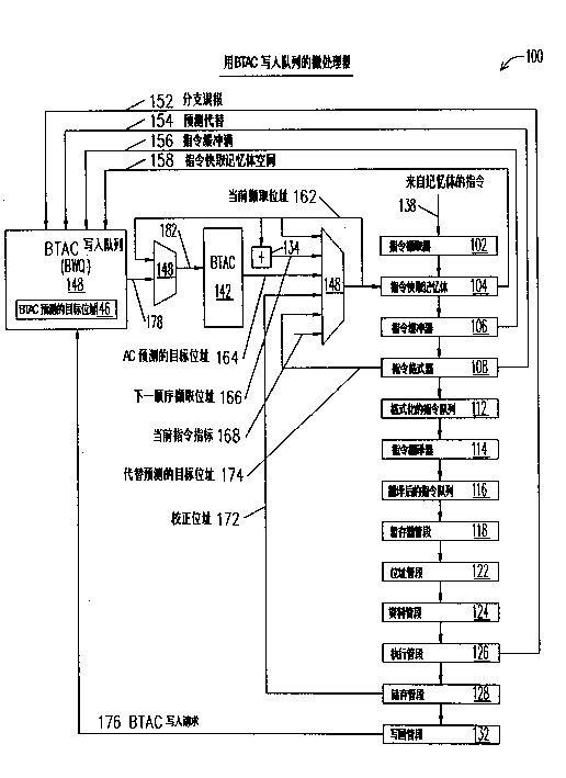
以下结合附图及较佳实施例,对依据本发明提出的解决分支目标地址快取中死结提取条件的装置与方法其具体结构、方法、步骤、特征及其功效,详细说明如后。Below in conjunction with the accompanying drawings and preferred embodiments, the specific structure, method, steps, features and effects of the device and method for solving deadlock extraction conditions in the branch target address cache according to the present invention are described in detail below.
请参阅图1所示,显示根据本发明的一微处理器100的方块图。该微处理器100包括一管线微处理器。Please refer to FIG. 1 , which shows a block diagram of a
微处理器100包括一指令撷取器102。指令撷取器102是从耦合至该微处理器100的一内存(比如,系统内存)撷取出指令138。在一实施例中,指令撷取器102从快取线的基本单位中的内存撷取指令。在一实施例中,指令是长度可变式指令。亦即,微处理器100的指令集内的所有指令的长度都不相同。在一实施例中,微处理器100包括指令集本质上兼容于指令长度可变的x86架构指令集的一微处理器。The
微处理器100也包括一指令快取104,耦合至指令撷取器102。指令快取104接收指令撷取器102输出的指令字节的快取线并快取该微处理器100后续所用的指令快取线。在一实施例中,指令快取104包括64KB的4向指令集联合L1快取。当一指令未命中于该指令快取104内时,指令快取104会通知指令撷取器102,其响应地从内存撷取包括该未命中指令的该快取线。一目前撷取地址162输入至指令快取104以选择快取线。在一实施例中,指令快取104内的快取线包括32字节。指令快取104也产生一指令快取闲置信号158。当指令快取104闲置时,指令快取104产生为真值的指令快取闲置信号158。当指令快取104未被读取时,指令快取104会闲置。在一实施例中,如果指令快取104未被读取,则该微处理器的BTAC142(将于底下详细讨论)也未被读取。The
微处理器100也包括一指令缓冲器106,耦合至指令快取104。指令缓冲器106从指令快取104接收指令字节的快取线并暂存该些快取线直到其被规格化成可被微处理器100执行的明确性指令。在一实施例中,指令缓冲器106包括4个项目(entry)以储存高达4条的快取线。指令缓冲器106产生指令缓冲器全满信号156。当指令缓冲器106全满时,指令缓冲器106产生为真的指令缓冲器全满信号156。在一实施例中,如果指令缓冲器1 06全满,则BTAC142不能被读取。The
微处理器100也包括一指令规格化器108,耦合至指令缓冲器106。该指令规格化器108从指令缓冲器106接收指令字节,并从而产生规格化指令。亦即,指令规格化器108检视指令缓冲器106内的一串指令字节,决定哪些字节包括下一指令与其长度,并输出下一指令与其长度。在一实施例中,规格化指令包括本质上兼容于x86架构指令集的指令。The
指令规格化器108也包括产生分支目标地址的逻辑电路,称为取代预测目标地址174。在一实施例中,分支目标地址产生逻辑电路包括一加法器,将一相对分支指令的偏差加至分支指令地址以产生取代预测目标地址174。在一实施例中,该逻辑电路包括一分支目标缓冲器以产生间接分支指令的目标地址。在一实施例中,该逻辑电路包括一呼叫/回传堆栈,以产生呼叫与回传指令的目标地址。该指令规格化器108也包括一预测取代信号154。指令规格化器108产生为真的预测取代信号154以取代该微处理器100内的BTAC142所做的分支预测,将在底下详细描述。亦即,如果指令规格化器108内的逻辑电路所产生的目标地址不符合BTAC142所产生目标地址,则指令规格化器108产生为真的预测取代信号154,以使得该BTAC142的预测所撷取的指令被放弃并使得微处理器100分支至该取代预测目标地址174。在一实施例中,在指令被放弃且微处理器100分支至该取代预测目标地址174的时间内,BTAC142不能被读取。
该微处理器100也包括一规格化指令队列112,耦合至指令规格化器108。规格化指令队列112接收从指令规格化器108输出的规格化指令并暂存该些规格化指令直到其被转译成微指令。在一实施例中,规格化指令队列112包括储存高达12个规格化指令的项目,虽然图12只显示出4个项目。The
该微处理器100也包括一指令转译器114,耦合至规格化指令队列112。指令转译器114将存于该规格化指令队列112内的该规格化指令转译成微指令。在一实施例中,微处理器100包括精简指令集计算机(reducedinstruction set computer,RISC)核心,其执行本身或精简指令集的微指令。The
该微处理器100也包括一转译后指令队列116,耦合至指令转译器114。转译后指令队列116接收从指令转译器114传来的转译后微指令并暂存该些微指令直到其可被其余微处理器的管线执行为止。The
该微处理器100也包括一缓存器阶段118,耦合至转译后指令队列116。缓存器阶段118包括复数缓存器以储存指令运算子与结果。缓存器阶段118包括使用者可视缓存器档案以储存微处理器100的使用者可视状态。The
该微处理器100也包括一地址阶段122,耦合至缓存器阶段118。地址阶段122包括地址产生逻辑电路,产生内存存取指令(比如加载或储存指令及分支指令)的内存地址。The
该微处理器100也包括一数据阶段124,耦合至地址阶段122。数据阶段124包括从内存加载数据的逻辑电路及快取从内存所加载数据之一或多快取。The
该微处理器100也包括一执行阶段126,耦合至数据阶段124。执行阶段126包括执行指令的执行单元,比如执行算数与逻辑指令的算数与逻辑单元。在一实施例中,执行阶段126包括整数执行单元,浮点执行单元,MMX执行单元与SSE执行单元。执行阶段126也包括分支指令决定逻辑电路。特别是,执行阶段126决定分支指令是否要执行及BTAC142先前误测的分支指令是否要执行。此外,执行阶段126决定BTAC142先前预测的分支目标地址是否被BTAC142误测,亦即是否不正确。如果执行阶段126决定先前分支预测是不正确的,执行阶段126产生为真值的分支误测信号152,以使得由于BTAC142误测所撷取的指令被放弃且使得该微处理器100分支至该正确地址172。在一实施例中,在指令被放弃且使得该微处理器100分支至该正确地址172的期间内,BTAC142不能被读取。The
该微处理器100也包括一储存阶段128,耦合至执行阶段126。储存阶段128包括响应于储存微指令而将数据存至内存的逻辑电路。储存阶段128产生一正确地址172。正确地址172包括分支指令的正确分支目标地址。亦即,正确地址172是分支指令的非预测性目标地址。当执行与确定分支指令时,正确地址172也写入至BTAC142,这将于底下详细描述。储存阶段128也产生一BTAC写入要求176以更新BTAC142。BTAC写入要求176将参阅图7做详细描述。The
该微处理器100也包括一写回阶段132,耦合至储存阶段128。写回阶段132包括将指令结果写至缓存器阶段118的逻辑电路。The
该微处理器100也包括BTAC142。BTAC142包括可快取目标地址与其它分支预测信息的高速缓存。BTAC142响应于从一多任务器148接收的一地址182而产生一预测目标地址164。在一实施例中,BTAC142包括单端口高速缓存,被BTAC142的读取与写入存取所共享,因而使得BTAC142有伪性未命中(false miss)的机率。BTAC142与多任务器148将于底下详述。The
该微处理器100也包括一第二多任务器136,耦合至BTAC142。多任务器136选择6个输入之一以输出成一目前撷取地址162。输入之一是由一加法器134所产生的一下一撷取地址166,加法器134对目前撷取地址162加上快取线的大小以产生该下一撷取地址166。在从指令快取104正常撷取一快取线后,多任务器136选择该下一撷取地址166以输出成该目前撷取地址162。另一输入是目前撷取地址162。另一输入是BTAC预测目标地址164,如果BTAC142指示一分枝指令存在于从该指令快取104的该目前撷取地址162所择出的该快取线内且BTAC142预测出该分支指令要被执行,则多任务器136选择BTAC预测目标地址164。另一输入是从储存阶段128接收的正确地址172,多任务器136选择正确地址172以校正一分支误测。另一输入是从指令规格化器108接收的取代预测目标地址174,多任务器136选择该取代预测目标地址174以取代该BTAC测试目标地址164。另一输入是一目前指令指针168,其指向目前正被该指令规格化器108规格化的指令的地址。多任务器136选择该目前指令指针168以避免死结情况,如下述。The
该微处理器100也包括一BTAC写入队列(BWQ)144,耦合至BTAC142。该BTAC写入队列144包括复数储存组件以暂存BTAC写入要求176,直到其可被写入至BTAC142为止。BTAC写入队列144接收该分支误测信号152,该预测取代信号154,该指令缓冲器全满信号156,与该指令快取闲置信号158。有利的是,BTAC写入队列144能利用BTAC写入要求176来延迟BTAC142的更新,直到输入信号152-158所指示的适当时间,亦即BTAC142未被读取的时间,以增加BTAC142的效率,将于底下详述。The
BTAC写入队列144产生一BTAC写入队列地址178,其输入至多任务器148。BTAC写入队列144也包括储存一目前队列深度146的一缓存器。队列深度146指出目前存于BWQ144内的有效BTAC写入要求176的数量。队列深度146的初始值为0。每次将一BTAC写入要求176存至BTAC写入队列144内,队列深度146都会增加。每次将一BTAC写入要求176从BWQ144移走,队列深度146都会减少。BTAC写入队列144将于底下详述。The
请参阅图2所示,显示根据本发明的图1的微处理器的部份详细方块图。图2显示BTAC写入队列144,BTAC142与图1的多任务器148,另增加一仲裁器202,以及耦合于该BTAC写入队列144与该BTAC142间之3-输入多任务器206。虽然图1的多任务器148只接收2个输入,多任务器148是4-输入多任务器,如图2所示。如图2所示,BTAC142包括一读/写输入,一地址输入与一数据输入。Please refer to FIG. 2, which shows a partial detailed block diagram of the microprocessor of FIG. 1 according to the present invention. FIG. 2 shows
请参阅图1所示,多任务器148接收该目前撷取地址162与该BWQ地址178。此外,多任务器148也接收一多余TA地址234与一死结地址236,将分别参阅第10-11图与第12-13图做详细描述。多任务器148根据该仲裁器202所产生的一控制信号258而选择其4个输入之一以输出成图1的一地址数据182,该地址数据182是输入至该BTAC142的该地址输入。Please refer to FIG. 1 , the
该多任务器206接收一多余TA数据信号244与一死结数据信号246,将分别参阅第10-11图与第12-13图做详细描述。多任务器206也接收从该BTAC写入队列144传来的一BWQ数据信号248,其为该目前BTAC写入队列144需要更新该BTAC142的数据。多任务器206根据该仲裁器202所产生的一控制信号262而选择三个输入之一以输出成一数据信号256,其输入至该BTAC142的数据输入。The multiplexer 206 receives an excess TA data signal 244 and a deadlock data signal 246, which will be described in detail with reference to FIGS. 10-11 and FIGS. 12-13, respectively. The multiplexer 206 also receives a BWQ data signal 248 from the
仲裁器202仲裁对该BTAC142要求存取的复数来源。当BTAC142被读或写时,仲裁器202产生一信号252至该BTAC142的该读/写输入以控制之。仲裁器202接收一BTAC读取要求信号212,其代表平行于也利用目前撷取地址162而对指令快取104的读取的利用目前撷取地址162而读取BTAC142之一要求。仲裁器202也接收一多余目标地址(TA)要求信号214,其代表要无效该BTAC142内的该多余TA地址234所选指令集内的相同分支指令之一多余项目之一要求,将于底下描述。仲裁器202也接收一死结要求信号216,其代表要将误测该死结地址236所选的指令集内之一分支指令未跨越快取边界线的该BTAC142内之一项目无效化之一要求,将于底下描述。仲裁器202也接收从该BTAC写入队列144输出之一BWQ非空信号218,其代表有待处理的至少一要求以更新该BWQ地址178所选指令集内的该BTAC142内之一项目,这将于底下描述。仲裁器202也接收从该BTAC写入队列144输出之一BWQ全满信号222,其代表该BTAC写入队列144填满了要更新该BWQ地址178所选指令集内的该BTAC142内之一项目的待处理要求,将于底下描述。The
在一实施例中,仲裁器202指定优先权,如底下表1所示,其中1代表最高优先权而5代表最低优先权:In one embodiment, the
1-死结要求2161- deadlock requirements 216
2-BMQ全满2222-BMQ full 222
3-BTAC读取要求2123-BTAC Read Requirement 212
4-多余TA要求2144- Redundant TA Requirement 214
5-BWQ非空2185-BWQ not empty 218
请参阅图3所示,显示根据本发明的图1的BTAC142的详细方块图。如图3,该BTAC142包括一目标地址数组302,一卷标数组304,与一计数器数组306。各数组302,304与306接收图1的地址182。图3的实施例显示4向指令集联合BTAC142高速缓存。在另一实施例中,BTAC142包括2向指令集联合高速缓存。在一实施例中,该目标地址数组302与该卷标数组304是单端口,但计数器数组306是具有一读取埠与一写入埠的双埠,因为计数器数组306的更新频率高于该目标地址数组302与该卷标数组304的更新频率。Please refer to FIG. 3, which shows a detailed block diagram of the BTAC142 of FIG. 1 according to the present invention. As shown in FIG. 3 , the
该目标地址数组302包括一储存组件数组,以储存能快取分支目标地址与相关分支预测信息的目标地址数组项目312。目标地址数组项目312的内容将参阅图4而于底下描述。该卷标数组304包括一储存组件数组,以储存可储存地址卷标与相关分支预测信息的卷标数组项目314。卷标数组项目314的内容将参阅图5而于底下描述。该计数器数组306包括一储存组件数组,以储存可储存分支结果预测信息的计数器数组项目316。计数器数组项目316的内容将参阅图6而于底下描述。The target address array 302 includes an array of storage elements for storing target address array entries 312 capable of caching branch target addresses and associated branch prediction information. The content of the target address array entry 312 will be described below with reference to FIG. 4 . The tag array 304 includes an array of storage elements for storing
各目标地址数组302,卷标数组304,与计数器数组306是规划成4向,如所示般之向0(way 0),向1(way 1),向2(way 2)与向3(way 3)。较好是,目标地址数组302之各向储存2个项目或一部份,以快取分支目标地址与预测性分支信息,由A与B代表,使得如果有两个分支指令存在于快取线内,BTAC142可预测出适当的分支指令。Each target address array 302, label array 304, and counter array 306 are planned into 4 directions, as shown, to 0 (way 0), to 1 (way 1), to 2 (way 2) and to 3 ( way 3). Preferably, each direction of the target address array 302 stores two entries or a portion to cache branch target addresses and predictive branch information, represented by A and B, such that if two branch instructions are present in the cache line Within, BTAC142 can predict the appropriate branch instruction.
各数组302-306由图1的地址182做索引。地址182的低位选择各数组302-306内的快取线。在一实施例中,各数组302-306包括128个指令集。因此,BTAC142能快取高达1024个目标地址,各指令集的各向(各指令集有4向)有2个地址。较好是,数组302-306由地址182之位[11:5]做索引以选择BTAC142内之4向指令集。Each array 302-306 is indexed by
请参阅图4所示,显示根据本发明的图3的目标地址数组项目312的内容。Please refer to FIG. 4 , which shows the contents of the target address array item 312 in FIG. 3 according to the present invention.
该目标地址数组项目312包括一分支目标地址(TA)402。在一实施例中,目标地址402包括32-位地址,从分支指令的先前执行快取得。BTAC142提供关于预测TA输出164的目标地址402。The target address array entry 312 includes a branch target address (TA) 402 . In one embodiment, the target address 402 includes a 32-bit address, fetched from a previous execution block of a branch instruction.
该目标地址数组项目312也包括一开始字段404。开始字段404代表响应于该目前撷取地址162而从该指令快取104输出之一快取线内的该分支指令的第一字节的字节偏差(byte offset)。在一实施例中,一快取线包括32字节;因此,开始字段404包括5位。The target address array entry 312 also includes a
该目标地址数组项目312也包括一跨越(wrap)位406。如果该预测分支指令是跨越指令快取104的两快取线的话,跨越位406为真。BTAC142提供关于B_wrap信号1214的跨越位406,将参阅图12而于底下讨论。The target address array entry 312 also includes a wrap bit 406 . The straddle bit 406 is true if the predicted branch instruction straddles two cache lines of the
请参阅图5所示,是显示根据本发明的图3的卷标数组项目314的内容。Please refer to FIG. 5 , which shows the content of the
该卷标数组项目314包括一卷标502。在一实施例中,卷标502包括该分支指令的地址的高阶20位,该分支指令使该目标地址数组302内的相关项目储存一预测目标地址402。如果该项目为有效的话,BTAC142比较标签502与图1的地址182的高阶20位以决定该项目是否匹配于地址182,亦即地址182是否命中于BTAC142内。The
该卷标数组项目314也包括一A有效位504,如果该目标地址数组302内的相关项目的A部份内的该目标地址402为有效的话,A有效位504为真。该卷标数组项目314也包括一B有效位506,如果该目标地址数组302内的相关项目的B部份内的该目标地址402为有效的话,该B有效位506为真。The
该卷标数组项目314也包括一3-位lru字段508,其指示所选指令集的该4向的哪一向是lru(Least Recently Used,最久未用)。在一实施例中,当执行BTAC分支时,BTAC142只更新该lru字段508。亦即,只有当BTAC142预测一分支指令将被执行且该微处理器100根据预测而分支至该BTAC142所提供的该预测目标地址164时,BTAC142才会更新该lru字段508。当BTAC分支正被执行时,于BTAC142未被读取且不需要使用BTAC写入队列144的期间内,BTAC142会更新lru字段508。The
请参阅图6所示,显示根据本发明的图3的计数器数组项目316的内容。Please refer to FIG. 6, which shows the content of the
计数器数组项目316包括一预测状态A计数器602。在一实施例中,该预测状态A计数器602是2-位饱和计数器,每次该微处理器100决定要执行相关分支指令时,其往上计数;每次不执行相关分支指令时,其往下计数。往上计数时,该预测状态A计数器602饱和于b`11的二进制值;往下计数时,该预测状态A计数器602饱和于b`00的二进制值。在一实施例中,如果该预测状态A计数器602的值是b`11或b`10,则BTAC142预测相关于所选目标地址数组项目312的A部份的分支指令要被执行;否则,BTAC142预测分支指令不要被执行。计数器数组项目316也包括一预测状态B计数器604,其操作相似于该预测状态A计数器602,但其相关于所选目标地址数组项目312的B部份。
计数器数组项目316也包括一A/Blru位606。A/Blru位606内的b`1的二进制值代表所选目标地址数组项目312的A部份是最久未用;否则,则是所选目标地址数组项目312的B部份是最久未用。在一实施例中,当分支指令到达会决定分支结果(亦即分支要执行与否)的该储存阶段128时,A/Blru位606连同该预测状态A与B计数器602与604一起被更新。在一实施例中,更新计数器数组项目316不需要使用到BTAC写入队列144,因为计数器数组306包括一读取端口与一写入埠,如图3所示。
请参阅图7所示,是显示根据本发明的图1的BTAC写入要求176的内容。图7显示输入至BTAC写入队列144的BTAC写入要求信号176内的由储存阶段128所产生的用于更新一BTAC142的项目的信息,其也是存于BTAC写入队列144的项目内的内容,如图8所示。Please refer to FIG. 7 , which shows the content of the
BTAC写入要求176包括一分支指令地址字段702,其是要更新该BTAC142的先前执行分支指令的地址。当该写入要求176接着更新BTAC142时,分支指令地址字段702的高阶20位是存至图5的卷标数组项目314的卷标字段502。分支指令地址字段702的低阶7位[11:5]是当成BTAC142的索引。在一实施例中,分支指令地址字段702是32-位字段。The
BTAC写入要求176也包括一开始字段708,以储存于图4的开始字段404内。BTAC写入要求176也包括一跨越位712,以储存于图4的跨越位406内。The
BTAC写入要求176也包括一写入致能A字段714,其代表是否要利用BTAC写入要求176指定的信息来更新所选目标地址数组项目312内的A部份。BTAC写入要求176也包括一写入致能B字段716,其代表是否要利用BTAC写入要求176指定的信息来更新所选目标地址数组项目312内的B部份。The
BTAC写入要求176也包括一无效A字段718,其代表是否要无效化所选目标地址数组项目312内的A部份。无效化所选目标地址数组项目312内的A部份是包括:清除图5的该A有效位504。BTAC写入要求176也包括一无效B字段722,其代表是否要无效化所选目标地址数组项目312内的B部份。无效化所选目标地址数组项目312内的B部份是包括:清除图5的该B有效位506。The
BTAC写入要求176也包括一4-位向字段724,其指定要更新所选指令集的四向的哪一向。向字段724是全解。在一实施例中,当微处理器100读取BTAC142以得到分支预测时,微处理器100决定要放于向字段724内之值并透过管线阶段而将该值往下送至储存阶段128以包含于该BTAC写入要求176内。如果微处理器100正在更新BTAC142内之一既有项目,亦即,如果目前撷取地址162命中于BTAC142内,微处理器100将既有项目之向设于向字段724内。如果微处理器100正在写入新项目于BTAC142内,比如,新分支指令,微处理器100将所选的BTAC142指令集的最久未用向设于向字段724内。在一实施例中,当微处理器100读取BTAC142以得到分支预测时,微处理器100从图5的lru字段508来决定最久未用向。The
请参阅图8所示,显示根据本发明的图3的BTAC写入队列144的方块图。Please refer to FIG. 8 , which shows a block diagram of the
BTAC写入队列144包括复数储存组件802以储存图7的BTAC写入要求176。在一实施例中,BTAC写入队列144包括6个储存组件802以储存6笔BTAC写入要求176,如所示。The
BTAC写入队列144也包括一有效位804,相关于各BTAC写入要求项目802;如果相关项目为有效,则有效位804为真;如果相关项目为无效,则有效位804为假。The
BTAC写入队列144也包括控制逻辑电路806,耦合至储存组件802与有效位804。控制逻辑电路806也耦合至队列深度缓存器146。当有一BTAC写入要求176加载至BTAC写入队列144时,控制逻辑电路806增加队列深度146;当BTAC写入要求176从BTAC写入队列144移出时,控制逻辑电路806减少队列深度146。控制逻辑电路806接收从图1的储存阶段128传来的BTAC写入要求信号176并将所接收的要求存于项目802。控制逻辑电路806也接收图1的分支误测信号152,预测取代信号154,指令缓冲器全满信号156与指令快取闲置信号158。当队列深度146大于0时,控制逻辑电路806产生为真的图2的BWQ非空信号218。当当队列深度146之值等于项目802的总数量(在图8的实施例中为8)时,控制逻辑电路806产生为真的图2的BWQ全满信号222。当控制逻辑电路806产生为真的BWQ非空信号218时,控制逻辑电路806将BTAC写入队列144的最旧(或最底部)项目802的分支指令地址702设于图1的BWQ地址信号178内。此外,当控制逻辑电路806产生为真的MWQ非空信号218时,控制逻辑电路806也将BTAC写入队列144的最旧(或最底部)项目802的图7的字段706-724设于BWQ数据信号248内。
请参阅图9所示,显示根据本发明的图1的BTAC写入队列144的操作流程图。流程开始于决定方块902。Please refer to FIG. 9 , which shows an operation flowchart of the
在决定方块902,BTAC写入队列144藉由决定图1的队列深度146是否等于BTAC写入队列144内的总项目数量来决定BTAC写入队列144是否全满。如果全满,流程跳至方块918以更新BTAC142;否则,流程跳至决定方块904。At
在决定方块904,BTAC写入队列144藉由检查该指令快取闲置信号158来决定图1的该指令快取104是否闲置。如果闲置,必要时,流程跳至决定方块922以更新BTAC142因为BTAC142可能未被读取;否则,流程跳至决定方块906。At
在决定方块906,BTAC写入队列144藉由检查该指令缓冲器全满信号156来决定图1的指令缓冲器106是否全满。如果全满,必要时,流程跳至决定方块922以更新BTAC142因为BTAC142可能未被读取;否则,流程跳至决定方块908。At
在决定方块908,BTAC写入队列144藉由检查该预测取代信号154来决定BTAC142分支预测是否已被取代。如果是,必要时,流程跳至决定方块922以更新BTAC142因为BTAC142可能未被读取;否则,流程跳至决定方块912。At
在决定方块912,BTAC写入队列144藉由检查该分支误测信号152来决定BTAC142分支预测是否已被校正。如果是,必要时,流程跳至决定方块922以更新BTAC142因为BTAC142可能未被读取;否则,流程跳至决定方块914。At
在决定方块914,BTAC写入队列144决定是否已产生该BTAC写入要求176。如果否,流程跳回至决定方块902;否则,流程跳至方块916。At
在决定方块916,BTAC写入队列144加载该BTAC写入要求176并增加队列深度146。该BTAC写入要求176被加载至BTAC写入队列144的最顶端的无效项目,接着该项目被标示为有效。流程跳回至决定方块902。At
在决定方块918,BTAC写入队列144利用BTAC写入队列144内的最旧或底部项目来更新BTAC142,并减少队列深度146。BTAC写入队列144接着往下移一个项目。藉由将最旧项目的图7的分支指令地址字段702之值设成BWQ地址信号178,以及将最旧BTAC写入要求176的其它部份设于BWQ数据信号248,BTAC写入队列144利用BTAC写入队列144内的最旧项目来更新BTAC142。此外,BTAC写入队列144发出为真的BWQ非空信号218至图2的仲裁器202。如果流程是从决定方块902跳至方块918,BTAC写入队列144也发出为真的BWQ全满信号2228至图2的仲裁器202。流程从方块918跳至决定方块914。At
要注意,如果在BTAC读取要求信号212也在待处理期间内,BTAC写入队列144发出该BWQ全满信号222且该仲裁器202允许BTAC写入队列144存取BTAC142;则BTAC142将会未命中,但如果BTAC142所预测的分支指令的有效目标地址存在于BTAC142内的目前撷取地址162所指定的快取线的话,此未命中是为伪性未命中。然而,有利的是,藉由在大部份情况下将BTAC142的写入延迟到BTAC142未被读取,BTAC写入队列144可降低BTAC142的伪性未命中的可能性,如图9所示。It should be noted that if the
在决定方块922,控制逻辑电路806藉由决定队列深度146是否等于0来决定是否BTAC写入队列144为空。如果是,流程跳至决定方块914;否则,流程跳至决定方块922以更新BTAC142因为BTAC142可能未被读取。At
请参阅图10所示,显示根据本发明的图1的该微处理器100内的将该BTAC内多余目标地址无效化的逻辑电路的方块图。Please refer to FIG. 10 , which shows a block diagram of a logic circuit for invalidating redundant target addresses in the BTAC in the
图10显示图3的BTAC142的卷标数组304接收图1的地址182并响应性产生4个标签,标示为tag0 1002A,tag1 1002B,tag2 1002C与tag31002D,总称为标签1002。卷标1002包括从卷标数组304的4向的各向传来的图5的标签502。此外,卷标数组304响应性产生8个有效位[7:0],标示为1004,其为从卷标数组304的4向的各向传来的A有效位504与B有效位506。FIG. 10 shows that the tag array 304 of the
微处理器100也包括比较器1012,耦合至卷标数组304,该比较器1012接收地址182。在图10的实施例中,比较器1012包括4个20-位比较器,各比较器比较地址182的高阶20位与相关卷标1002以产生四个匹配信号,标示为match0 1006A,matchl 1006B,match2 1006C与match3 1006D,总称为匹配信号1006。如果地址182匹配于相关卷标1002,则比较器1012产生为真值的匹配信号1006。The
微处理器100也包括控制逻辑电路1014,耦合至比较器1012,该电路1014接收匹配信号1006与有效信号1004。如果卷标数组304的所选指令集的向中有复数向具有为真值的匹配信号1006与至少一个为真值的有效位1004,则控制逻辑电路1014储存一真值于多余TA旗标缓存器1024内,以代表同一分支指令的一个以上的有效目标地址是存于BTAC142内。此外,控制逻辑电路1014使得地址182加载至于多余TA地址缓存器1026内。最后,控制逻辑电路1014加载多余TA无效数据至多余TA无效数据缓存器1022内。在一实施例中,存于多余TA无效数据缓存器1022内的数据是相似于图7的BTAC写入要求176,除了未储存分支指令地址702外,因为该分支指令的地址是存于多余TA地址缓存器1026内;且也未储存目标地址706,开始位708,与跨越位712,因为其在无效BTAC142项目内是无关紧要的;因而,当进行多余TA无效化时,目标地址数组302不会被写入,而只有卷标数组304被更新以无效该多余BTAC142项目。该多余TA无效数据缓存器1022的输出包括图2的多余TA无效数据信号244。该多余TA旗标缓存器1024的输出包括图2的多余TA要求214。该多余TA地址缓存器1026的输出包括图2的多余TA地址234。在一实施例中,存于该多余TA无效数据缓存器1022与该多余TA旗标缓存器1024内的该向值724的产生等式是显示于底下的表2。在表2中,有效位[3]包括A有效位[3]504与B有效位[3]506的逻辑OR结果;有效位[2]包括A有效位[2]504与B有效位[2]506的逻辑OR结果;有效位[1]包括A有效位[1]504与B有效位[1]506的逻辑OR结果;以及有效位[0]包括A有效位[0]504与B有效位[0]506的逻辑OR结果。The
RedundantInvalWay[3]=(valid[3] & match[3]) & ((valid[0] & match[0])|(valid[1] & match[1])|(valid[2] & match[2]));RedundantInvalWay[3]=(valid[3] & match[3]) & ((valid[0] & match[0])|(valid[1] & match[1])|(valid[2] & match[ 2]));
RedundantInvalWay[2]=(valid[2] & match[2]) & ((valid[0] & match[0])|(valid[1]&match[1]));RedundantInvalWay[2]=(valid[2] & match[2]) & ((valid[0] &match[0])|(valid[1]&match[1]));
Redundant InvalWay[1]=(valid[1] & match[1]) & (valid[0] & match[0]);Redundant InvalWay[1] = (valid[1] & match[1]) & (valid[0] &match[0]);
Redundant InvalWay[0]=0;/*Way 0永远不会被无效*/Redundant InvalWay[0] = 0; /*
RedundanInAFlag=((valid[3] & match[3]) & (valid[2] & match[2]))|RedundanInAFlag=((valid[3] & match[3]) & (valid[2] & match[2]))|
((valid[3] & match[3]) & (valid[1] & match[1]))|((valid[3] & match[3]) & (valid[1] & match[1]))|
((valid[3] & match[3]) & (valid[0] & match[0]))|((valid[3] & match[3]) & (valid[0] & match[0]))|
((valid[2] & match[2]) & (valid[1] & match[1]))|((valid[2] & match[2]) & (valid[1] & match[1]))|
((valid[2] & match[2]) & (valid[0] & match[0]))|((valid[2] & match[2]) & (valid[0] & match[0]))|
((valid[1] & match[1]) & (valid[0] & match[0]));((valid[1] & match[1]) & (valid[0] &match[0]));
为使图10的多余目标地址无效逻辑电路的适当操作,如图11所示,将一串的指令执行为例做说明,其可在BTAC142内产生同一分支指令的多余目标地址项目。In order to properly operate the redundant target address invalidation logic circuit in FIG. 10, as shown in FIG. 11, a series of instructions are executed as an example to illustrate, which can generate redundant target address entries of the same branch instruction in the BTAC142.
图1的第一目前撷取地址162是输入至指令快取104与BTAC142。第一目前撷取地址162所选的快取线包括一分支指令,称为分支-A。第一目前撷取地址162选择BTAC142内之一指令集,称为指令集N。指令集N的向内没有一个标签1002匹配于第一目前撷取地址162;因此,BTAC142产生未命中。在此例中,lru值508所代表的最久未用向是2。因此,关于分支-A的更新BTAC142的信息是沿着管线往下送,连同代表向2必需被更新的分支-A。The first current fetch
接着,输入一第二目前撷取地址162至该指令快取104与BTAC142。由第二目前撷取地址162所选的快取线包括一分支指令,称为分支-B。第二目前撷取地址162也选择指令集N且命中于指令集N的3向;接着,BTAC142产生一命中。此外,BTAC142更新指令集N的lru值508为1向。Next, input a second current fetch
接着,因为分支-A是码的紧凑循环的一部份,再次输入该第一目前撷取地址162至该指令快取104与BTAC142,并再次选择指令集N。因为分支-A的第一次执行未到达图1的储存阶段128,BTAC142未利用分支-A的目标地址做更新。接着,BTAC142再次产生未命中。然而,此次的lru值508所指的最久未用向是1,因为lru508响应于分支-B的命中而被更新。因此,关于分支-A的第二次执行的更新BTAC142的信息是沿着管线往下送,连同代表向1必需被更新的分支-A的第二次执行。Next, since branch-A is part of a tight loop of code, the first current fetch
接着,该第一分支-A到达该储存阶段128并产生一BTAC写入要求176以利用分支-A的目标地址来更新指令集N的向2,这将于后续进行。Next, the first branch-A reaches the
接着,该第二分支-A到达该储存阶段128并产生一BTAC写入要求176以利用分支-A的目标地址来更新指令集N的向1,这将在后续进行。因此,同一分支指令,分支-A,的两个有效项目存在于BTAC142内。该些项目之一是多余的且造成BTAC142的使用较无效率,因为该多余项目可以被另一分支指令使用及/或会占去另一分支指令的有效目标地址。Next, the second branch-A reaches the
请参阅图11所示,显示根据本发明的图10的多余目标地址装置的操作流程图。流程开始于方块1102。Please refer to FIG. 11 , which shows an operation flow chart of the redundant target address device in FIG. 10 according to the present invention. Flow begins at block 1102 .
在方块1102,仲裁器202允许图2的BTAC读取要求212对BTAC142的存取,造成多任务器148选择目前撷取地址162以设于图1的地址信号182上并产生图2的控制信号252以代表BTAC142的读取。接着,目前撷取地址162的低阶位透过地址182而当成选择BTAC142的指令集的索引。流程接续至方块1104。At block 1102, the
在方块1104,比较器1012比较所选BTAC142的指令集的所有4个向的图10的卷标1002与设于地址信号182上的目前撷取地址162的高阶位以产生图10的匹配信号1006。控制逻辑电路1014接收图10的匹配信号1006与有效位1004。流程接续至方块1106。At block 1104, the comparator 1012 compares the tag 1002 of FIG. 10 for all four directions of the instruction set of the selected
在方块1106,控制逻辑电路1014决定是否发生一个以上的有效标签匹配。亦即,根据有效位1004与匹配信号1006,控制逻辑电路1014决定是否有目前撷取地址162所选的BTAC142的指令集内的2个以上的向有一有效匹配标签1002。如果是,流程接续至方块1108;否则,流程结束。At block 1106, the
在方块1108,控制逻辑电路1014储存一真值于多余TA旗标缓存器1024,储存地址182于多余TA地址缓存器1026,以及储存无效数据于多余TA无效数据缓存器1022。特别是,控制逻辑电路1014储存为真值的写入致能A字段714、写入致能B字段716、无效A字段718与无效B字段722于多余TA无效数据缓存器1022。此外,控制逻辑电路1014将根据图10所描述的表2的向字段724之值存于多余TA无效数据地址缓存器1022。流程接续至方块1112。At block 1108 , the
在方块1112,仲裁器202允许图2的多余TA要求214对BTAC142的存取,造成多任务器148选择多余TA地址234以设于地址信号182上且产生图2的控制信号252以指示BTAC142的写入。接着,多余TA地址234的低阶位透过地址182而当成选择BTAC142的指令集的索引。BTAC142接收多余TA数据缓存器1022所输出的多余数据信号244并将所选指令集内的向字段724所指向的该些向无效化。流程结束于方块1112。At block 1112, the
请参阅图12所示,显示根据本发明的该微处理器100内的死结避免逻辑电路的方块图。Please refer to FIG. 12 , which shows a block diagram of the deadlock avoidance logic circuit in the
图12显示图1的BTAC142,指令快取104,指令缓冲器106,指令格式器108,格式后指令队列112与多任务器136,以及图10的控制逻辑电路1014。FIG. 12 shows the
如图12所示,微处理器100也包括一死结无效数据缓存器1222,一死结旗标缓存器1224,与一死结地址缓存器1226。As shown in FIG. 12 , the
指令格式器108译码存于该指令缓冲器106内的指令,以及如果指令格式器108译码出跨越两快取线的分支指令,则产生为真的F_wrap信号1202。特别是,在指令格式器108译码出跨越两快取线的分支指令时,一旦已译码出存于指令缓冲器106内的一第一快取线内的一跨越分支指令的该第一部份,不论指令格式器108是否已译码尚未存于指令缓冲器106内的该第二快取线内的该跨越分支指令的其它部份,指令格式器108产生为真的F_wrap信号1202。F_wrap信号1202是输入至控制逻辑电路1014。The
当目前撷取地址162未命中时,指令快取104产生为真值的未命中信号1206。未命中信号1206是输入至控制逻辑电路1014。I-
当输入至指令快取104的目前撷取地址162是预测的,亦即,当目前撷取地址162是一预测性地址时,指令快取104产生为真值的一预测信号1208,比如当多任务器136选择BTAC预测目标地址164为目前撷取地址162时。预测信号1208是输入至指令快取104。在一实施例中,指令快取104将预测信号1208送至图1的指令撷取器102,使得指令撷取器102放弃从内存的预测内存地址处撷取未命中于指令快取104内的快取线,理由将参阅图13而于底下描述。The
BTAC142产生一执行/不执行(T/NT)信号1212,其输出至控制逻辑电路1014。为真值的T/NT信号1212代表地址182命中于BTAC142内,代表BTAC142预测一分支指令是包括于响应于目前撷取地址162而由指令快取104提供的快取线内,代表该分支指令要被执行,以及代表BTAC142将分支指令的目标地址设于BTAC预测目标地址信号164上。BTAC142根据图6的预测状态A 602或预测状态B 604之值而产生T/NT信号1212,取决于该BTAC142在分支预测时是使用A或B部份。
BTAC142也产生B_wrap信号1214,输出至控制逻辑电路1014。所选的BTAC目标地址数组项目312的图4的跨越位406之值是设成B_wrap信号1214。因此,B_wrap信号1214的伪值代表,BTAC142预测成该分支指令未跨越于两快取线。在一实施例中,控制逻辑电路1014暂存B_wrap信号1214以维持从先前BTAC142存取所得的B_wrap信号1214之值。The
控制逻辑电路1014也产生图1的目前指令指针168。控制逻辑电路1014也产生一控制信号1204,其是多任务器136的输入选择信号。The
如果控制逻辑电路1014侦测出死结状态(亦即,所暂存的B_wrap信号1214为伪值,与F_wrap信号1202、未命中信号1206与预测信号1208为真值),这将于底下详述,则控制逻辑电路1014储存一真值于一死结旗标缓存器1224内以代表现在有死结状态,使得造成死结状态的BTAC142内的项目被无效。此外,控制逻辑电路1014加载死结无效数据至死结无效数据缓存器1222内。在一实施例中,存于死结无效数据缓存器1222内的数据是相似于图7的BTAC写入要求176;除了未储存分支指令地址702外,因为该分支指令的地址是存于死结地址缓存器1226内;以及未储存目标地址706,开始位708与跨越位712,因为在一无效BTAC142项目内,这些位是无关紧要的;因而,当执行死结无效化时,目标地址数组302未被写入,而只有卷标数组304被更新以将误测的BTAC142的项目无效化。死结无效数据缓存器1222的输出包括图2的死结数据信号246。死结旗标缓存器1224的输出包括图2的死结要求216。死结地址缓存器1226的输出包括图2的死结地址236。存于死结无效数据缓存器1222内的该向值724是由造成该死结状态的该BTAC142的该向填入。If the
如果控制逻辑电路1014侦测出死结状态,则在将误测项目无效化后,控制逻辑电路1014也产生一值于控制信号1204上以使得该多任务器1306选择该目前指令指针168以造成微处理器100的分支,使得包括该误测分支指令的该快取线可被再次撷取。If the
请参阅图13所示,显示根据本发明的图12的死结避免逻辑电路的操作流程图。流程开始于方块1302。Please refer to FIG. 13 , which shows an operation flowchart of the dead-knot avoidance logic circuit of FIG. 12 according to the present invention. Flow begins at block 1302 .
在方块1302,目前撷取地址162是经由地址信号182而输入至指令快取104与输入至BTAC142。在图13中,该目前撷取地址162是称为撷取地址A。流程接续至方块1304。At block 1302 , the currently fetched
在方块1304,指令快取104将撷取地址A所指定的快取线(称为快取线A)提供至指令缓冲器106,快取线A包括分支指令的第一部份,但并无包括该分支指令的全部。流程接续至方块1306。At
在方块1306,响应于撷取地址A,BTAC142预测快取线A内的分支指令将被执行并设于T/NT信号1212上,产生为伪值的B_wrap信号1214,并将一预测目标地址设于BTAC预测目标地址164上。流程接续至方块1308。At
在方块1308,控制逻辑电路1014控制多任务器136以选择BTAC预测目标地址164为下一个目前撷取地址162,称为撷取地址B。控制逻辑电路1014也产生为真值的预测信号1208,因为BTAC预测目标地址164是预测性的。流程接续至方块1312。At
在方块1312,指令快取104产生为真值的未命中信号1206以代表分支地址B是未命中于指令快取104内。正常下,指令撷取器102可能从内存撷取该未命中快取线;然而,因为预测信号1208为真,指令格式器108并不内存撷取该未命中快取线,理由将于底下描述。流程接续至方块1314。At
在方块1314,指令格式器108译码指令缓冲器106内的快取线A并产生为真值的F_wrap信号1202,因为该分支指令跨越两快取线。指令格式器108等待要存于指令缓冲器106内的下一快取线,使得其可完成对分支指令的格式以将的输出至格式后指令队列112。流程接续至方块1316。At
在方块1316,控制逻辑电路1014决定:所暂存的B_wrap信号1214是否为伪值,F_wrap信号1202是否为真值,未命中信号1206是否为真值与预测信号1208是否为真值;这包括了底下所描述的死结状态。如果是,流程接续至方块1318;否则,流程结束。At
在方块1318,控制逻辑电路1014将造成死结状态的该BTAC142项目无效化,如参阅图12所述。接着,当下次将撷取地址A输入至BTAC142时,BTAC142将产生一未命中,因为造成死结状态的该项目现已被无效化。流程接续至方块1322。At
在方块1322,控制逻辑电路1014控制多任务器136以分支至目前指令指针168,如参阅图12的描述。此外,当控制逻辑电路1014控制该多任务器136选择目前指令指针168时,控制逻辑电路1014产生为伪值的预测信号1208,因为目前指令指针168不是预测性内存地址。很可能目前指令指针168会命中于指令快取104内;然而,如果没命中的话,指令撷取器102将从内存撷取目前指令指针168所指定的快取线,因为预测信号1208代表目前指令指针168不是预测性。流程结束于方块1322。At
如果决定方块1316为真时,存在有死结状态的理由在于,造成死结的必要情况是存在的。造成死结的第一情况是跨越于两不同快取线的多字节分支指令。亦即,该分支指令字节的第一部份是位于第一快取线的尾端,而该分支指令字节的第二部份是位于下一快取线的开端。因为跨越分支指令的可能性,该BTAC142必需储存预测一分支指令是否跨越快取线的信息,使得控制逻辑电路1014得知是否要撷取下一快取线以在撷取位于目标地址164的快取线之前就取得分支指令字节的下半部。如果BTAC142储存了错误的预测信息,BTAC142可能会错误地预测为该分支指令未跨越,但实际上有跨越。在此例下,该指令格式器108将利用分支指令的前半部来译码该快取线并侦测出已存在有一分支指令,但并非分支指令的全部字节已可用于译码。该指令格式器108会等待下一快取线。该管线会一直等待要被格式的更多指令以将的执行。If
造成死结情况的第二情况是,因为该BTAC142预测该分支指令未跨越,该分支控制逻辑电路1014撷取该BTAC142输出的目标地址164所暗指的快取线(并无撷取下一快取线)。然而,该目标地址164未命中于该指令快取104内。因此,该指令格式器108所等待的下一快取线必需从内存撷取。The second situation that creates a deadlock situation is that, because the
造成死结情况的第三情况是,微处理器的芯片组并无预期到会有从某些内存地址范围内撷取出指令,以及如果该微处理器从未预期的内存地址范围产生指令撷取时,微处理器的芯片组可能会使得系统闲置或产生其它不良的系统情况。预测性地址,比如BTAC142所输出的目标地址164,可能会从未预期的内存地址范围造成指令撷取。因而,该微处理器100并无从内存之一预测性BTAC预测目标地址164撷取一未命中快取线。A third situation that creates a deadlock situation is when the microprocessor's chipset does not anticipate fetches from certain memory address ranges, and if the microprocessor generates an instruction fetch from an unanticipated memory address range , the microprocessor's chipset may idle the system or create other undesirable system conditions. Predictive addresses, such as
因此,指令格式器108与管线的其它部份是等待另一快取线。同时,该指令撷取器102是等待该管线以告知要执行一非预测性撷取。在非死结情况下,比如,如果该目标地址164命中于指令快取104内,指令格式器108会将分支指令格式(虽然是利用不正确的字节)与将格式后的分支指令提供至分支的执行阶段,执行阶段会侦测出误测并将BTAC142的误测校正,因而使得该预测信号1208变成伪值。然而,在死结情况下,该执行将永远无法侦测出误测,因为指令格式器108未将格式后的分支指令提供至分支的执行阶段,因为指令格式器108仍在等待下一快取线。因此,发生死结情况。然而,图12的死结避免逻辑电路可有效避免死结情况的发生,如图12与图13所述,因而使得微处理器100可适当操作。Therefore, the
虽然已详细描述本发明与其目的,特征与优点,本发明仍可包括其它实施例。比如,虽然该写入队列是相关于单端口BTAC,在某些微处理器架构中,伪性未命中也可能发生于多端口BTAC中,尽管频率较低。因此,可应用该写入队列以减少多端口BTAC的伪性未命中率。此外,在未读取BTAC的某些微处理器中,可能也有除了在此所描述情况外的其它情况,其中队列于该写入队列内的要求可写入至BTAC。While the invention and its objects, features and advantages have been described in detail, the invention can still include other embodiments. For example, although the write queue is relative to a single-port BTAC, spurious misses may also occur, albeit less frequently, in a multi-port BTAC in some microprocessor architectures. Therefore, the write queue can be applied to reduce the spurious miss rate of the multi-port BTAC. Furthermore, in some microprocessors that do not read the BTAC, there may be other situations than those described here where requests queued in the write queue can be written to the BTAC.
另,虽然已详细描述本发明与其目的,特征与优点,本发明仍可包括其它实施例。除了利用硬件来实施本发明外,本发明也可实施于计算机可用式(比如,可读式)媒介内的计算机可读码(比如,计算机可读程序代码,数据等)。计算机码可完成所揭露的本发明的功能或制造或两者皆可。比如,可利用一般程序语言(比如,C,C++,JAVA等);GDSII数据库;硬件描述语言(hard description language,HDL),包括Verilog HDL,VHDL,AlteraHDL(AHDL)等;或现有的其它程序及/或电路(亦即概要式)撷取工具。计算机码可加载于包括半导体内存,磁盘,光盘(比如,CD-ROM,DVD-ROM等)的任意习知计算机可用式(比如,可读式)媒介内;以及以计算机数据信号的形式实施于计算机可用式(比如,可读式)传输媒介(比如,载波,或包括数字,光学或模拟式媒介的其它媒介)。因此,计算机码可传输于包括因特网与企业网络(指令tranet)通讯网路上。要知道,本发明可实施于计算机码(比如,IP(智财权)核心之一部份,比如为微处理器核心,或为系统级设计,比如系统单芯片(SOC))与转换成集成电路的部份硬件。另,本发明可实施成硬件与计算机码的组合。Additionally, while the invention and its objects, features and advantages have been described in detail, the invention can still include other embodiments. Instead of implementing the invention in hardware, the invention can also be embodied in computer readable code (eg, computer readable program code, data, etc.) on a computer usable (eg, readable) medium. The computer code may perform the function or manufacture or both of the disclosed invention. For example, general programming language (such as C, C++, JAVA, etc.) can be utilized; GDSII database; hardware description language (hard description language, HDL), including Verilog HDL, VHDL, AlteraHDL (AHDL), etc.; or existing other programs and/or circuit (ie abstract) extraction tools. The computer code can be loaded in any known computer usable (eg, readable) medium including semiconductor memory, magnetic disk, optical disk (eg, CD-ROM, DVD-ROM, etc.); and implemented in the form of a computer data signal Computer-usable (eg, readable) transmission media (eg, carrier waves, or other media including digital, optical or analog media). Thus, computer code can be transmitted over communication networks including the Internet and corporate networks (command tranets). It will be appreciated that the present invention can be implemented in computer code (e.g., part of an IP (intellectual property) core, such as a microprocessor core, or in a system-level design, such as a system-on-a-chip (SOC)) and converted into an integrated circuit part of the hardware. Alternatively, the present invention can be implemented as a combination of hardware and computer code.
以上所述,仅是本发明的较佳实施例而已,并非对本发明作任何形式上的限制,虽然本发明已以较佳实施例揭露如上,然而并非用以限定本发明,任何熟悉本专业的技术人员,在不脱离本发明技术方案范围内,当可利用上述揭示的方法及技术内容作出些许的更动或修饰为等同变化的等效实施例,但是凡是未脱离本发明技术方案的内容,依据本发明的技术实质对以上实施例所作的任何简单修改、等同变化与修饰,均仍属于本发明技术方案的范围内。The above description is only a preferred embodiment of the present invention, and does not limit the present invention in any form. Although the present invention has been disclosed as above with preferred embodiments, it is not intended to limit the present invention. Anyone familiar with this field Those skilled in the art, without departing from the scope of the technical solution of the present invention, can use the method and technical content disclosed above to make some changes or modifications to equivalent embodiments with equivalent changes, but any content that does not depart from the technical solution of the present invention, Any simple modifications, equivalent changes and modifications made to the above embodiments according to the technical essence of the present invention still fall within the scope of the technical solutions of the present invention.
Claims (19)
Applications Claiming Priority (2)
| Application Number | Priority Date | Filing Date | Title |
|---|---|---|---|
| US44006203P | 2003-01-14 | 2003-01-14 | |
| US60/440,062 | 2003-01-14 |
Publications (2)
| Publication Number | Publication Date |
|---|---|
| CN1521635A true CN1521635A (en) | 2004-08-18 |
| CN100397365C CN100397365C (en) | 2008-06-25 |
Family
ID=34312105
Family Applications (1)
| Application Number | Title | Priority Date | Filing Date |
|---|---|---|---|
| CNB2004100005482A Expired - Lifetime CN100397365C (en) | 2003-01-14 | 2004-01-14 | Device and method for solving deadlock extraction condition in branch target address cache |
Country Status (2)
| Country | Link |
|---|---|
| CN (1) | CN100397365C (en) |
| TW (1) | TWI242744B (en) |
Cited By (6)
| Publication number | Priority date | Publication date | Assignee | Title |
|---|---|---|---|---|
| CN100407137C (en) * | 2004-12-17 | 2008-07-30 | 国际商业机器公司 | Branch lookahead prefetch for microprocessors |
| CN104106046A (en) * | 2012-02-14 | 2014-10-15 | 瑞萨电子株式会社 | Data processing device |
| CN106919367A (en) * | 2016-04-20 | 2017-07-04 | 上海兆芯集成电路有限公司 | The processor and method of detecting modification program code |
| CN111459551A (en) * | 2020-04-14 | 2020-07-28 | 上海兆芯集成电路有限公司 | Microprocessor with highly advanced branch predictor |
| CN112579175A (en) * | 2020-12-14 | 2021-03-30 | 海光信息技术股份有限公司 | Branch prediction method, branch prediction device and processor core |
| CN113504941A (en) * | 2020-11-13 | 2021-10-15 | 圣图尔科技公司 | Spectre repair method and microprocessor using predictor mode label |
Families Citing this family (3)
| Publication number | Priority date | Publication date | Assignee | Title |
|---|---|---|---|---|
| US7434033B2 (en) * | 2006-04-14 | 2008-10-07 | International Business Machines Corporation | Placing a processor into a gradual slow mode of operation in response to a detected livelock condition within a processor pipeline |
| TWI509408B (en) * | 2013-01-23 | 2015-11-21 | Realtek Semiconductor Corp | Deadlock detection method and machine readable medium |
| TWI739556B (en) * | 2020-08-19 | 2021-09-11 | 瑞昱半導體股份有限公司 | Clock deadlock detection system, method, and non-transitory computer readable medium thereof |
Family Cites Families (5)
| Publication number | Priority date | Publication date | Assignee | Title |
|---|---|---|---|---|
| US6895498B2 (en) * | 2001-05-04 | 2005-05-17 | Ip-First, Llc | Apparatus and method for target address replacement in speculative branch target address cache |
| US7134005B2 (en) * | 2001-05-04 | 2006-11-07 | Ip-First, Llc | Microprocessor that detects erroneous speculative prediction of branch instruction opcode byte |
| US6823444B1 (en) * | 2001-07-03 | 2004-11-23 | Ip-First, Llc | Apparatus and method for selectively accessing disparate instruction buffer stages based on branch target address cache hit and instruction stage wrap |
| US7162619B2 (en) * | 2001-07-03 | 2007-01-09 | Ip-First, Llc | Apparatus and method for densely packing a branch instruction predicted by a branch target address cache and associated target instructions into a byte-wide instruction buffer |
| TW564369B (en) * | 2001-07-16 | 2003-12-01 | Ip First Llc | Apparatus and method for handling BTAC branches that wrap across instruction cache lines |
-
2004
- 2004-01-13 TW TW093100763A patent/TWI242744B/en not_active IP Right Cessation
- 2004-01-14 CN CNB2004100005482A patent/CN100397365C/en not_active Expired - Lifetime
Cited By (10)
| Publication number | Priority date | Publication date | Assignee | Title |
|---|---|---|---|---|
| CN100407137C (en) * | 2004-12-17 | 2008-07-30 | 国际商业机器公司 | Branch lookahead prefetch for microprocessors |
| CN104106046A (en) * | 2012-02-14 | 2014-10-15 | 瑞萨电子株式会社 | Data processing device |
| CN104106046B (en) * | 2012-02-14 | 2018-05-15 | 瑞萨电子株式会社 | Data processing equipment |
| CN106919367A (en) * | 2016-04-20 | 2017-07-04 | 上海兆芯集成电路有限公司 | The processor and method of detecting modification program code |
| CN106919367B (en) * | 2016-04-20 | 2019-05-07 | 上海兆芯集成电路有限公司 | Processor and method for detecting self-correcting code |
| CN111459551A (en) * | 2020-04-14 | 2020-07-28 | 上海兆芯集成电路有限公司 | Microprocessor with highly advanced branch predictor |
| CN111459551B (en) * | 2020-04-14 | 2022-08-16 | 上海兆芯集成电路有限公司 | Microprocessor with highly advanced branch predictor |
| CN113504941A (en) * | 2020-11-13 | 2021-10-15 | 圣图尔科技公司 | Spectre repair method and microprocessor using predictor mode label |
| CN112579175A (en) * | 2020-12-14 | 2021-03-30 | 海光信息技术股份有限公司 | Branch prediction method, branch prediction device and processor core |
| CN112579175B (en) * | 2020-12-14 | 2023-03-31 | 成都海光微电子技术有限公司 | Branch prediction method, branch prediction device and processor core |
Also Published As
| Publication number | Publication date |
|---|---|
| TWI242744B (en) | 2005-11-01 |
| TW200416603A (en) | 2004-09-01 |
| CN100397365C (en) | 2008-06-25 |
Similar Documents
| Publication | Publication Date | Title |
|---|---|---|
| CN1303536C (en) | Microprocessor and apparatus for performing fast speculative load operation | |
| CN100342326C (en) | Multi-threaded processor and method for manipulating the processor | |
| CN1217262C (en) | Appts. and method for replacing target address in imaginary branch target address high speed buffer storage | |
| CN100342349C (en) | Out-of-pipeline trace buffer for instruction replay following misspeculation | |
| CN1220938C (en) | Double regualting return stack branch predicting system | |
| CN1257452C (en) | Appts. system and method of imaginary branch target address high speed buffer storage branch | |
| CN1260646C (en) | Imaginary branch target address high speed buffer storage attached with secondary predictor | |
| CN1147794C (en) | Decoupling instruction fetch-actuating engine with static jump prediction support | |
| CN1210649C (en) | Scheduler capable of issuing and reissuing dependency chains | |
| CN1217271C (en) | Imaginary branch target address high speed buffer storage | |
| CN1153133C (en) | Information processing device by using small scale hardware for high percentage of hits branch foncast | |
| CN1269030C (en) | Appts. and method for quick fetching line selecting target address of high speed buffer storage | |
| CN1387641A (en) | Multithreaded Execution in Parallel Processors | |
| CN1641567A (en) | Method and apparatus for performing fast speculative pop operation from a stack memory cache | |
| CN1934543A (en) | Cache memory and control method thereof | |
| CN1178942A (en) | Self-parallelization with register renaming | |
| CN1658154A (en) | Pipeline microprocessor device and method for early correction of branch instruction prediction errors | |
| CN1629801A (en) | Pipelined microprocessor, apparatus and method for generating early instruction results | |
| CN1521635A (en) | Device and method for solving deadlock extraction condition in branch target address cache | |
| CN1282930C (en) | Apparatus and method for efficiently updating branch target address cache | |
| CN1967506A (en) | Coalescing entries in cache memory processors | |
| CN100339825C (en) | Device and method for invalidating redundant items in branch target address cache | |
| CN1797326A (en) | Control circuit and its control method | |
| CN1449521A (en) | Computer system | |
| CN1279782A (en) | Computer system |
Legal Events
| Date | Code | Title | Description |
|---|---|---|---|
| C06 | Publication | ||
| PB01 | Publication | ||
| C10 | Entry into substantive examination | ||
| SE01 | Entry into force of request for substantive examination | ||
| C14 | Grant of patent or utility model | ||
| GR01 | Patent grant | ||
| CX01 | Expiry of patent term | ||
| CX01 | Expiry of patent term |
Granted publication date: 20080625 |