CN1528078A - Allocation of Packet Descriptor Field Locations in Network Processors - Google Patents
Allocation of Packet Descriptor Field Locations in Network Processors Download PDFInfo
- Publication number
- CN1528078A CN1528078A CNA028050126A CN02805012A CN1528078A CN 1528078 A CN1528078 A CN 1528078A CN A028050126 A CNA028050126 A CN A028050126A CN 02805012 A CN02805012 A CN 02805012A CN 1528078 A CN1528078 A CN 1528078A
- Authority
- CN
- China
- Prior art keywords
- memory
- frame
- fcb
- data
- information
- Prior art date
- Legal status (The legal status is an assumption and is not a legal conclusion. Google has not performed a legal analysis and makes no representation as to the accuracy of the status listed.)
- Granted
Links
Images


Classifications
-
- H—ELECTRICITY
- H04—ELECTRIC COMMUNICATION TECHNIQUE
- H04L—TRANSMISSION OF DIGITAL INFORMATION, e.g. TELEGRAPHIC COMMUNICATION
- H04L49/00—Packet switching elements
- H04L49/90—Buffering arrangements
- H04L49/9047—Buffering arrangements including multiple buffers, e.g. buffer pools
-
- H—ELECTRICITY
- H04—ELECTRIC COMMUNICATION TECHNIQUE
- H04L—TRANSMISSION OF DIGITAL INFORMATION, e.g. TELEGRAPHIC COMMUNICATION
- H04L49/00—Packet switching elements
- H04L49/90—Buffering arrangements
-
- H—ELECTRICITY
- H04—ELECTRIC COMMUNICATION TECHNIQUE
- H04L—TRANSMISSION OF DIGITAL INFORMATION, e.g. TELEGRAPHIC COMMUNICATION
- H04L47/00—Traffic control in data switching networks
- H04L47/50—Queue scheduling
-
- H—ELECTRICITY
- H04—ELECTRIC COMMUNICATION TECHNIQUE
- H04L—TRANSMISSION OF DIGITAL INFORMATION, e.g. TELEGRAPHIC COMMUNICATION
- H04L49/00—Packet switching elements
- H04L49/90—Buffering arrangements
- H04L49/901—Buffering arrangements using storage descriptor, e.g. read or write pointers
Landscapes
- Engineering & Computer Science (AREA)
- Computer Networks & Wireless Communication (AREA)
- Signal Processing (AREA)
- Data Exchanges In Wide-Area Networks (AREA)
- Communication Control (AREA)
- Liquid Developers In Electrophotography (AREA)
- Input Circuits Of Receivers And Coupling Of Receivers And Audio Equipment (AREA)
- Glass Compositions (AREA)
- Computer And Data Communications (AREA)
Abstract
一种降低为获得帧控制块中的所需字段信息,访问存储器的次数的方法和系统。在一个实施例中,系统包括处理数据帧的处理器。处理器可包括接收和传输数据帧的数据流单元,每个数据帧可具有相关的帧控制块。每个帧控制块包含第一和第二控制块。处理器还可包括与数据流单元耦接,保存第一控制块的字段信息的第一存储器。处理器还可包括与数据流单元耦接的调度器,其中调度器被配置成调度数据流单元接收的数据帧。调度器可包括保存第二控制块的字段信息的第二存储器。A method and system to reduce the number of times memory is accessed to obtain required field information in a frame control block. In one embodiment, a system includes a processor that processes frames of data. The processor may include a data flow unit that receives and transmits data frames, each data frame may have an associated frame control block. Each frame control block contains first and second control blocks. The processor may further include a first memory coupled to the data flow unit and storing field information of the first control block. The processor may also include a scheduler coupled to the data streaming unit, wherein the scheduler is configured to schedule data frames received by the data streaming unit. The scheduler may include a second memory storing field information of the second control block.
Description
技术领域technical field
本发明涉及连网通信系统领域,更具体地说,涉及使对存储器的访问次数降至最小。This invention relates to the field of networked communication systems and, more particularly, to minimizing the number of memory accesses.
背景技术Background technique
分组交换网络具有用于在与网络相连的发送器和接收器之间传输数据的交换点或交换节点。这些交换点执行的交换事实上是把交换点或节点接收的数据的分组或“帧”传给网络中的另一节点的操作。这种交换操作是借助其通过分组交换网络转移通信数据的手段。Packet-switched networks have switching points or switching nodes for transferring data between senders and receivers connected to the network. The switching performed by these switching points is in fact the operation of passing packets or "frames" of data received by the switching point or node to another node in the network. This switching operation is the means by which communication data is transferred over a packet-switched network.
每个节点可以包括配置成处理数据分组或帧的分组处理器。每个数据帧可与配置成描述相关数据帧的帧控制块(FCB)有关。通常,FCB包括各种信息字段,信息字段由分组处理器中的存储器,例如四元数据速率静态随机存取存储器(QDR SRAM)提供。即,通过访问分组处理器中的存储器,例如QDR SRAM,获得FCB中的信息字段。Each node may include a packet processor configured to process data packets or frames. Each data frame may be associated with a frame control block (FCB) configured to describe the associated data frame. Typically, the FCB includes various information fields provided by memory in the packet processor, such as Quad Data Rate Static Random Access Memory (QDR SRAM). That is, the information fields in the FCB are obtained by accessing memory in the packet processor, such as QDR SRAM.
于是,希望限制字段控制块中需要信息的字段的数目,从而减少存储器访问次数,提高存储器空间效率,即存储器的带宽的效率。Therefore, it is desirable to limit the number of fields that require information in the field control block, thereby reducing the number of memory accesses and improving memory space efficiency, that is, memory bandwidth efficiency.
发明内容Contents of the invention
本发明提供一种表现为第一和第二控制块的逻辑字段控制块(FCB),第一控制块与第一存储器相关,第二控制块与第二存储器相关。每个存储器,即第一和第二存储器还可分别和分组处理器的一个数据流单元和一个调度器相关。分组处理器的数据流单元可被配置成接收并传送数据帧。分组处理器的调度器可被配置成调度要传送给分组交换网络中的另一交换机或端口的数据帧。当FCB驻留在数据流单元中的一个队列中时,信息可保存在第一控制块的字段中,而不是保存在第二控制块的字段中。由于不访问第二存储器来相对于第二控制块的字段进行读取/写入操作,因此提高了第二存储器的带宽效率。当FCB驻留在调度器中的一个队列中时,信息可保存在第二控制块的字段中,而不是保存在第一控制块的字段中。由于不访问第一存储器来相对于第一控制块的字段进行读取/写入操作,因此提高了第一存储器的带宽效率。The invention provides a logical field control block (FCB) in the form of a first control block and a second control block, the first control block being associated with a first memory and the second control block being associated with a second memory. Each memory, ie the first and the second memory, may also be associated with a dataflow unit and a scheduler of the packet processor, respectively. The dataflow unit of the packet processor may be configured to receive and transmit data frames. The scheduler of the packet processor may be configured to schedule data frames to be transmitted to another switch or port in the packet switched network. When the FCB resides in one of the queues in the data flow unit, the information may be stored in the fields of the first control block instead of in the fields of the second control block. Bandwidth efficiency of the second memory is improved since the second memory is not accessed for read/write operations with respect to fields of the second control block. When the FCB resides in a queue in the scheduler, the information may be stored in fields of the second control block instead of fields of the first control block. Bandwidth efficiency of the first memory is improved since the first memory is not accessed for read/write operations with respect to fields of the first control block.
根据一方面,本发明提供一种系统,包括:处理数据帧的处理器,其中所述处理器包括:接收和传输所述数据帧的数据流单元,其中每个所述数据帧具有相关的帧控制块,每个所述帧控制块包括第一和第二控制块;与所述数据流单元耦接的第一存储器,其中所述第一存储器包括第一帧缓冲器控制单元,其中所述第一帧缓冲器控制单元保存所述帧控制块的所述第一控制块的字段信息;和与所述数据流单元耦接的调度器,其中所述调度器调度所述数据流单元接收的数据帧,其中所述调度器包括第二存储器,其中所述第二存储器包括第二帧缓冲器控制单元,所述第二帧缓冲器控制单元保存所述帧控制块的所述第二控制块的字段信息。According to one aspect, the present invention provides a system comprising: a processor for processing frames of data, wherein said processor includes: a data streaming unit for receiving and transmitting said frames of data, wherein each of said frames of data has an associated frame control blocks, each of said frame control blocks comprising first and second control blocks; a first memory coupled to said data streaming unit, wherein said first memory comprises a first frame buffer control unit, wherein said The first frame buffer control unit saves the field information of the first control block of the frame control block; and a scheduler coupled with the data flow unit, wherein the scheduler schedules the data received by the data flow unit data frames, wherein the scheduler includes a second memory, wherein the second memory includes a second frame buffer control unit that holds the second control block of the frame control block field information.
最好,数据流单元包括若干队列,其中一个或多个所述帧控制块驻留在所述若干队列之一中。在优选实施例中,驻留于所述数据流单元的所述若干队列之一中的一个或多个所述帧控制块的所述第一控制块的字段中的信息保存在所述第一存储器的所述第一帧缓冲器控制单元中。Advantageously, the dataflow unit comprises several queues, wherein one or more of said frame control blocks resides in one of said several queues. In a preferred embodiment, information in fields of said first control block of one or more of said frame control blocks residing in one of said number of queues of said dataflow unit is stored in said first memory in the first framebuffer control unit.
适宜地,调度器包括第一队列,其中一个或多个所述帧控制块驻留在所述第一队列中。更适宜的是,驻留在所述第一队列中的一个或多个所述帧控制块的所述第二控制块的字段中的信息保存在所述第二存储器的所述第二帧缓冲器控制单元中。Suitably, the scheduler includes a first queue, wherein one or more of said frame control blocks reside in said first queue. Preferably, information in fields of said second control block of one or more of said frame control blocks residing in said first queue is stored in said second frame buffer of said second memory in the controller control unit.
根据另一方面,本发明提供一种降低为获得帧控制块中的所需信息,访问存储器的次数的方法,其中每个所述帧控制块包括第一控制块和第二控制块,其中所述第一控制块与第一存储器相关,所述第二控制块与第二存储器相关,所述第一存储器包括第一帧缓冲器控制单元,所述第一帧缓冲器控制单元保存所述帧控制块的所述第一控制块的字段信息,所述第二存储器包括第二帧缓冲器控制单元,所述第二帧缓冲器控制单元保存所述帧控制块的所述第二控制块的字段信息,所述方法包括下述步骤:访问所述第一存储器,以便读取或写入一个或多个所述帧控制块的所述第一控制块的字段中的信息;和访问所述第二存储器,以便读取或写入一个或多个所述帧控制块的所述第二控制块的字段中的信息。According to another aspect, the present invention provides a method of reducing the number of memory accesses to obtain required information in frame control blocks, wherein each of said frame control blocks comprises a first control block and a second control block, wherein said The first control block is associated with a first memory, the second control block is associated with a second memory, the first memory includes a first frame buffer control unit, and the first frame buffer control unit stores the frame Field information of the first control block of the control block, the second memory includes a second frame buffer control unit, and the second frame buffer control unit stores the field information of the second control block of the frame control block field information, said method comprising the steps of: accessing said first memory to read or write information in a field of said first control block of one or more of said frame control blocks; and accessing said A second memory for reading or writing information in fields of said second control block of one or more of said frame control blocks.
可取的是,一个或多个所述帧控制块驻留在数据流单元中的若干队列之一中,其中所述数据流单元与所述第一存储器相关。更优选的是,当所述一个或多个帧控制块驻留在所述数据流单元中的所述若干队列之一中时,访问第一存储器,以便读取或写入一个或多个所述帧控制块的所述第一控制块的字段中的信息。最好,一个或多个所述帧控制块驻留在调度器中的一个队列中,其中所述调度器与所述第二存储器相关。适宜的是,当所述一个或多个帧控制块驻留在所述调度器的所述队列中时,访问第二存储器,读取或写入一个或多个所述帧控制块的所述第二控制块的字段中的信息。Advantageously, one or more of said frame control blocks reside in one of several queues in a dataflow unit associated with said first memory. More preferably, when said one or more frame control blocks reside in one of said number of queues in said data flow unit, accessing the first memory to read or write one or more of said frame control blocks information in a field of said first control block of said frame control block. Advantageously, one or more of said frame control blocks reside in a queue in a scheduler associated with said second memory. Suitably, when said one or more frame control blocks reside in said queue of said scheduler, accessing a second memory reads or writes said Information in the fields of the second control block.
根据另一方面,本发明提供一种保存在计算机可读存储介质上的计算机程序产品,当在计算机系统上运行时,指令计算机系统实现如上所述的系统。According to another aspect, the present invention provides a computer program product stored on a computer readable storage medium, which, when run on a computer system, instructs the computer system to implement the system as described above.
附图说明Description of drawings
下面参考附图中图解说明的本发明的优选实施例,举例说明本发明,其中:The invention is illustrated below with reference to the preferred embodiments of the invention which are illustrated in the accompanying drawings, in which:
图1图解说明根据本发明配置的分组处理器;Figure 1 illustrates a packet processor configured in accordance with the present invention;
图2图解说明根据本发明配置的数据流单元;Figure 2 illustrates a data flow unit configured in accordance with the present invention;
图3是降低为获得帧控制块中的所需信息,访问存储器的次数的方法的流程图;3 is a flowchart of a method for reducing the number of memory accesses to obtain required information in a frame control block;
图4图解说明本发明的驻留在数据流单元的FCB自由队列中的FCB的基本FCB的一个实施例;Figure 4 illustrates an embodiment of the basic FCB of the present invention of FCBs residing in the FCB free queue of the data flow unit;
图5图解说明本发明的驻留在数据流单元的FCB自由队列中的FCB的流式FCB的一个实施例;Figure 5 illustrates an embodiment of the streaming FCB of the present invention with FCBs residing in the FCB free queue of the data streaming unit;
图6图解说明本发明的驻留在数据流单元的GQ中的FCB的基本FCB的一个实施例;Figure 6 illustrates an embodiment of the basic FCB of the present invention residing in the GQ of the FCB in the data flow unit;
图7图解说明本发明的驻留在数据流单元的GQ中的FCB的流式FCB的一个实施例;Figure 7 illustrates one embodiment of the streaming FCB of the present invention for FCBs residing in the GQ of the data streaming unit;
图8图解说明本发明的驻留在调度器的流队列中的FCB的基本FCB的一个实施例;Figure 8 illustrates one embodiment of the basic FCB of the present invention for FCBs residing in the flow queues of the scheduler;
图9图解说明本发明的驻留在调度器的流队列中的FCB的流式FCB的一个实施例;FIG. 9 illustrates one embodiment of a streaming FCB of an FCB residing in a scheduler's flow queue of the present invention;
图10图解说明本发明的驻留在数据流单元的TBQ中的FCB的基本FCB的一个实施例;Figure 10 illustrates one embodiment of the basic FCB of the FCB residing in the TBQ of the data flow unit of the present invention;
图11图解说明本发明的驻留在数据流单元的TBQ中的FCB的流式FCB的一个实施例。Figure 11 illustrates one embodiment of the streaming FCB of the present invention for FCBs residing in a TBQ of a data streaming unit.
具体实施方式Detailed ways
本发明提供一种降低为获得帧控制块中所需字段信息,访问存储器的次数的方法和系统。在本发明的一个实施例中,系统包括配置成处理数据帧的处理器。处理器可包括配置成接收和传送数据帧的数据流单元,每个数据帧可以具有相关的帧控制块。每个帧控制块可包括第一和第二控制块。处理器还可包括与数据流单元耦接的第一存储器,第一存储器包括第一帧缓冲器控制单元。第一帧缓冲器控制单元可保存帧控制块的第一控制块的字段信息。处理器还可包括与数据流单元耦接的调度器,调度器被配置成调度数据流单元接收的数据帧。调度器可包括第二存储器,第二存储器包括第二帧缓冲器控制单元。第二帧缓冲器控制单元可保存帧控制块的第二控制块的字段信息。当帧控制块排队驻留在数据流单元中时,信息可保存在第一控制块的字段中,而不是保存在第二控制块的字段中。由于未访问第二存储器来相对于第二控制块中的字段进行读/写操作,因此提高了第二存储器的带宽的效率。当帧控制块排队驻留在调度器中时,信息可保存在第二控制块的字段中,而不是保存在第一控制块的字段中。由于未访问第一存储器来相对第一控制块中的字段进行读/写操作,因此提高了第二存储器的带宽的效率。The present invention provides a method and system for reducing the number of memory accesses required to obtain required field information in a frame control block. In one embodiment of the invention, a system includes a processor configured to process frames of data. The processor may include a data flow unit configured to receive and transmit data frames, each data frame may have an associated frame control block. Each frame control block may include first and second control blocks. The processor may further include a first memory coupled to the data streaming unit, the first memory including a first frame buffer control unit. The first frame buffer control unit may save field information of the first control block of the frame control block. The processor may also include a scheduler coupled to the data streaming unit, the scheduler being configured to schedule data frames received by the data streaming unit. The scheduler may include a second memory including a second frame buffer control unit. The second frame buffer control unit may save field information of the second control block of the frame control block. When frame control blocks are queued to reside in a data flow unit, information may be stored in fields of a first control block rather than in fields of a second control block. Since the second memory is not accessed for read/write operations with respect to fields in the second control block, bandwidth efficiency of the second memory is increased. When a frame control block is queued to reside in the scheduler, the information may be stored in fields of the second control block instead of in fields of the first control block. Since the first memory is not accessed for read/write operations relative to fields in the first control block, bandwidth efficiency of the second memory is increased.
图1图解说明了分组处理器100。分组处理器100可包括数据流单元110,数据流单元110被配置成从分组交换网络的特定交换机(未示出)或者端口(未示出)接收数据的数字分组,即数据帧,并把数据的数字分组,即数据帧传送给分组交换网络中的另一交换机或端口,例如交换机/端口120。每个数据帧可与一个帧控制块(FCB)相关,FCB描述数据的相关帧。与一个数据帧相关的每个FCB可和一个或多个缓冲器控制块(BCB)相关,与FCB相关的每个BCB可与数据存储单元140中的一个缓冲器相关。BCB可被配置成描述与下一链接的BCB相关的缓冲器,如同在美国专利申请序列号09/791336(代理人索引RAL000095下的同时待审PCT申请)中描述的那样。在一个实施例中,数据流单元10可驻留在集成电路,即集成芯片上。数据流单元110可与数据存储单元140耦接,数据存储单元140被配置成临时保存数据流单元110从分组交换网络中的一个交换机(未示出)或端口(未示出)接收的数据帧。数据流单元110还可与调度器130耦接,调度器130被配置成调度将从数据流单元110传送给交换机/端口120的数据帧。在一个实施例中,调度器130可驻留在集成电路,即集成芯片上。此外,数据流单元110还可与嵌入式处理器150耦接,嵌入式处理器150被配置成处理数据流单元110接收的数据帧。FIG. 1 illustrates a packet processor 100 . Packet processor 100 may include a data flow unit 110 configured to receive digital packets of data, i.e., data frames, from a particular switch (not shown) or port (not shown) of a packet-switched network, and transfer the data The digital packets, ie, data frames, are transmitted to another switch or port in the packet-switched network, such as switch/port 120. Each frame of data may be associated with a frame control block (FCB), which describes the associated frame of data. Each FCB associated with a data frame may be associated with one or more buffer control blocks (BCBs), and each BCB associated with an FCB may be associated with a buffer in the data storage unit 140 . The BCB can be configured to describe the buffer associated with the next linked BCB, as described in US Patent Application Serial No. 09/791336 (co-pending PCT application under Attorney Index RAL000095). In one embodiment, the
图2更详细地说明了数据流单元110。数据流单元110可包括接收器控制器203,接收器控制器203被配置成接收和临时保存从分组交换网络中的交换机(未示出)或者端口(未示出)接收的数据分组,即数据帧。数据流单元110还可包括发射器控制器201,发射器控制器201被配置成修改帧数据,并把修改后的帧数据传送给分组交换网络中的交换机(未示出)或者端口(未示出)。数据流单元110还可包括嵌入式处理器接口控制器202,嵌入式处理器接口控制器202被配置成交换要被嵌入式处理器150处理的帧。Figure 2 illustrates the dataflow unit 110 in more detail. The data flow unit 110 may include a receiver controller 203 configured to receive and temporarily store data packets received from switches (not shown) or ports (not shown) in the packet-switched network, ie, data frame. The data flow unit 110 may also include a transmitter controller 201 configured to modify the frame data and transmit the modified frame data to a switch (not shown) or a port (not shown) in the packet switching network. out). The dataflow unit 110 may also include an embedded processor interface controller 202 configured to switch frames to be processed by the embedded processor 150 .
数据分组,即数据帧可由端口/交换机接口单元221接收。当数据流单元110按照输出(engress)模式工作时,端口/交换机接口单元221可从分组交换网络中的交换机(未示出)接收数据。否则,当数据流单元110按照输入(ingress)模式工作时,端口/交换机接口单元221可从用作到分组交换网络的接口的端口(未示出)接收数据。在被保存在数据存储单元140中之前,数据流单元110接收的数据可临时保存在接收预备区存储器220中,数据存储器单元140可由若干切片(slice)205AF表示。切片205AF可整体地或者单独地分别称为切片205。图2中的切片205的数目是例证性的,根据本发明的数据流单元110的实施例可具有其它预定数目的切片205。每个切片可包括若干缓冲器。每个切片可代表一片存储器,例如动态随机存取存储器(DRAM),从而帧数据可被写入不同切片中的不同缓冲器中,以使存储器带宽达到最大。存储器判优器204可被配置成收集来自于接收器控制器203、发射器控制器201和嵌入式处理器接口控制器202的请求,例如读取请求、写入请求,随后调度对特定数据存储存储器切片,即特定切片205中的特定缓冲器的访问。例如,接收器控制器203可被配置成向存储器判优器204发出写入请求,以便把接收的数据写入特定切片205中的各个缓冲器中。Data packets, ie data frames, may be received by the port/switch interface unit 221 . When the data flow unit 110 operates in an ingress mode, the port/switch interface unit 221 can receive data from a switch (not shown) in the packet switching network. Otherwise, the port/switch interface unit 221 may receive data from a port (not shown) used as an interface to a packet-switched network when the data flow unit 110 operates in an ingress mode. The data received by the data streaming unit 110 may be temporarily stored in the receiving reserve area storage 220 before being stored in the data storage unit 140, which may be represented by several slices (slices) 205AF. Slices 205AF may be collectively or individually referred to as slices 205 , respectively. The number of slices 205 in FIG. 2 is illustrative, and embodiments of the data flow unit 110 according to the present invention may have other predetermined numbers of slices 205 . Each slice may include several buffers. Each slice may represent a slice of memory, such as dynamic random access memory (DRAM), such that frame data may be written to different buffers in different slices to maximize memory bandwidth. The memory arbiter 204 can be configured to collect requests from the receiver controller 203, the transmitter controller 201, and the embedded processor interface controller 202, such as read requests, write requests, and then schedule requests for specific data storage A memory slice, that is, an access to a specific buffer in a specific slice 205 . For example, the receiver controller 203 may be configured to issue a write request to the memory arbiter 204 to write received data into various buffers in a particular slice 205 .
如上所述,帧数据可保存在数据存储单元140,即若干切片205中。在一个实施例中,帧数据可以这样的方式保存在一个或多个切片205中的一个或多个缓冲器中,以致可通过使缓冲器链接在一起,重新组合每个特定帧中的数据。即,特定帧中的数据可保存在按照数据写入其中的顺序链接在一起的一个或多个缓冲器中。一个或多个缓冲器的链接可由与数据流单元110耦接的存储器229,例如四元数据速率静态随机存取存储器(QDR SRAM),中的缓冲器控制块单元(BCBU)208控制。BCBU 208可被配置成包括按照数据写入其中的顺序链接在一起的一个或多个缓冲器的地址。借助保存在BCBU208中的指针,可把包含相同帧的数据的不同缓冲器链接在一起。As mentioned above, frame data may be stored in data storage unit 140 , ie, number of slices 205 . In one embodiment, frame data may be stored in one or more buffers in one or more slices 205 in such a manner that the data in each particular frame can be reassembled by chaining the buffers together. That is, the data in a particular frame may be held in one or more buffers that are linked together in the order in which the data was written. Linking of one or more buffers may be controlled by buffer control block unit (BCBU) 208 in memory 229 coupled to dataflow unit 110 , such as a quad data rate static random access memory (QDR SRAM). BCBU 208 may be configured to include addresses for one or more buffers that are linked together in the order in which data is written therein. By means of pointers stored in BCBU 208, different buffers containing data for the same frame can be linked together.
如上所述,每个数据帧可与一个帧控制块(FCB)相关,FCB描述数据的相关帧。存储器210,例如QDR SRAM,中的帧控制块单元1(FCBU1)209可被配置成保存要填入FCB的字段中的信息,例如帧控制信息。即,可通过访问存储器210,即存储器210的FCBU1 209,获得FCB中的信息字段。在图3的说明中讨论了和保存信息字段的存储器210的FCBU1 209相关的其它细节。As noted above, each frame of data may be associated with a frame control block (FCB), which describes the associated frame of data. Frame Control Block Unit 1 (FCBU1) 209 in memory 210, such as QDR SRAM, may be configured to hold information to be filled into fields of the FCB, such as frame control information. That is, the information field in the FCB can be obtained by accessing the memory 210, that is, the FCBU1 209 of the memory 210. Additional details related to FCBU1 209 of memory 210 holding information fields are discussed in the description of FIG. 3 .
通过把要处理的各帧的报头传送给嵌入式处理器150,保存在缓冲器中的帧数据可被嵌入式处理器150处理。如上所述,每帧数据可由一个FCB表示。这些FCB可临时保存在G队列(GQ)218中。分配器逻辑电路217可被配置成使下一FCB从GQ 218出列。一旦分配器逻辑电路217使下一FCB出列,那么分配器逻辑电路217向存储器判优器204发出读取请求,以便读取位于保存在与出列FCB相关的数据存储单元140中的帧的起点(即该帧报头)中的数据。嵌入式处理器150随后处理分配器逻辑电路217读取的数据。The frame data held in the buffer can be processed by the embedded processor 150 by transmitting the header of each frame to be processed to the embedded processor 150 . As described above, each frame of data can be represented by one FCB. These FCBs may be temporarily held in G Queue (GQ) 218 . Allocator logic 217 may be configured to dequeue the next FCB from GQ 218. Once the next FCB is dequeued by the allocator logic 217, the allocator logic 217 issues a read request to the memory arbiter 204 to read the frame stored in the data storage unit 140 associated with the dequeued FCB. The data in the starting point (that is, the header of this frame). Embedded processor 150 then processes the data read by distributor logic 217 .
一旦嵌入式处理器150处理了帧数据,那么向存储器判优器204发出把处理后的帧数据写入一个或多个切片205中的各个缓冲器中的写入请求的嵌入式处理器逻辑电路216,可把处理后的帧数据临时保存在数据存储单元140,即切片205中。Once the embedded processor 150 has processed the frame data, the embedded processor logic issues a write request to the memory arbiter 204 to write the processed frame data to each buffer in one or more slices 205 216. Temporarily store the processed frame data in the data storage unit 140, that is, in the slice 205.
一旦嵌入式处理器150处理了帧数据,那么嵌入式处理器逻辑电路216还向调度器130发出与处理后的帧相关的FCB。调度器130可被配置成包括保存FCB的流队列223。调度器130还可包括位于存储器224,例如QDR SRAM内的帧控制块单元2(FCBU2)225,FCBU2 225被配置成类似于FCBU1 209工作。FCBU2 225可被配置成当FCB临时驻留于流队列223中时,保存要填入FCB的字段中的信息。在图3的说明中讨论了和保存信息字段的调度器130的存储器224内的FCBU2 225相关的其它细节。调度器130可被配置成把保存在流队列223中的FCB传送给目标刀形(blade)队列(TBQ)列队(enqueue)逻辑电路227,TBQ列队逻辑电路227被配置成把接收的FCB排列到TBQ 215中。Once embedded processor 150 has processed the frame data, embedded processor logic 216 also issues an FCB associated with the processed frame to scheduler 130 . The scheduler 130 may be configured to include a flow queue 223 that holds FCBs. The scheduler 130 may also include a frame control block unit 2 (FCBU2) 225 located in memory 224, such as QDR SRAM, configured to operate similarly to FCBU1 209. FCBU2 225 may be configured to hold information to be filled in fields of an FCB when the FCB is temporarily resident in the flow queue 223. Additional details related to the FCBU2 225 within the memory 224 of the scheduler 130 holding the information fields are discussed in the description of FIG. 3 . Scheduler 130 may be configured to transfer FCBs held in flow queues 223 to target blade queue (TBQ) enqueue logic 227, which is configured to enqueue received FCBs to TBQ 215 in.
在TBQ 215中列队的FCB可由TBQ调度器228安排成从TBQ215出列,并被载入端口控制块(PCB)224中。TBQ调度器228可被配置成使下一FCB从TBQ 215出列,并把该FCB排列到PCB224中。一旦下一FCB被排列到PCB 224中,那么PCB 224可向存储器判优器204发出读取请求,以便读取位于保存在与出列FCB相关的数据存储单元140中的帧的起点(即帧报头)中的数据。在把处理后的帧数据传送给分组交换网络中的交换机(未示出)或者端口(未示出)之前,PCB 224读取的数据可临时保存在数据预备区存储器214中。为清楚起见,注意PCB 224可被配置成在每个特定读取请求中,读取保存在处理后的帧中的一部分数据。即,可在PCB 224提供的多个读取请求中读取保存在处理后的帧中的整个数据。一旦读取了保存在处理后的帧中的整个数据,那么数据存储单元140可保存另外的帧数据。FCBs queued in TBQ 215 may be scheduled by TBQ scheduler 228 to be dequeued from TBQ 215 and loaded into port control block (PCB) 224. TBQ scheduler 228 may be configured to dequeue the next FCB from TBQ 215 and queue that FCB into PCB 224. Once the next FCB is queued into PCB 224, PCB 224 may issue a read request to memory arbiter 204 to read the beginning of the frame (i.e. frame header) in the data. Before transmitting the processed frame data to a switch (not shown) or a port (not shown) in the packet switching network, the data read by the PCB 224 can be temporarily stored in the data reserve memory 214. For clarity, note that the PCB 224 can be configured to read a portion of the data held in the processed frame in each particular read request. That is, the entire data stored in the processed frame can be read in multiple read requests provided by the PCB 224. Once the entire data stored in the processed frame is read, the data storage unit 140 may store additional frame data.
发射器控制器201还可包括帧改变预备区存储器213,帧改变预备区存储器213被配置成接收修改临时保存在数据预备区存储器214中的处理帧的命令。这些命令通常称为由嵌入式处理器150发出,并由嵌入式处理器逻辑216保存在特定缓冲器的特定存储区中的帧修改命令,如美国专利申请序列号09/792557中更详细说明的那样。在一个实施例中,PCB 224可被配置成取回保存在特定缓冲器的特定存储区中的帧修改命令,并把这些命令保存在帧改变预备区存储器213中。帧改变(FA)逻辑单元212可被配置成执行保存在帧改变预备区存储器213中的命令,以修改临时保存在数据预备区存储器214中的处理帧的内容。一旦FA逻辑单元212修改了处理帧的内容,那么可通过交换机/端口接口单元211传送修改后的处理帧。当数据流单元110按照输出模式工作时,交换机/端口接口单元211可把数据传送给用作到分组交换网络的接口的端口(未示出)。否则,当数据流单元110按照输入模式工作时,交换机/端口接口单元211可把数据传送给分组交换网络中的交换机(未示出)。The transmitter controller 201 may further include a frame change staging area memory 213 configured to receive a command to modify a processed frame temporarily stored in the data staging area memory 214 . These commands are generally referred to as frame modification commands issued by the embedded processor 150 and held by the embedded processor logic 216 in a particular memory area of a particular buffer, as described in more detail in U.S. Patent Application Serial No. 09/792,557 like that. In one embodiment, the PCB 224 may be configured to retrieve frame modification commands stored in a specific memory area of a specific buffer and store these commands in the frame change staging area memory 213. The frame change (FA) logic unit 212 may be configured to execute commands stored in the frame change reserve memory 213 to modify the contents of the processed frames temporarily stored in the data reserve memory 214 . Once the FA logic unit 212 modifies the content of the processed frame, the modified processed frame may be transmitted through the switch/port interface unit 211 . When the data flow unit 110 is operating in an output mode, the switch/port interface unit 211 may transmit data to a port (not shown) used as an interface to a packet-switched network. Otherwise, the switch/port interface unit 211 may transmit the data to a switch (not shown) in the packet switching network when the data flow unit 110 is operating in the input mode.
数据流单元110还可包括缓冲器控制块(BCB)判优器207,缓冲器控制块判优器207被配置成仲裁来自发射器控制器201、嵌入式处理器接口控制器202和接收器控制器203的不同BCB请求,以便相对于BCBU 208进行读取或写入操作。BCB判优器207可被配置成调度不同的访问,以便尽可能高效地利用存储器带宽。数据流单元110还可包括帧控制块(FCB)判优器206,FCB判优器206被配置成仲裁来自嵌入式处理器接口控制器202、接收器控制器203和发射器控制器201的不同FCB,以便相对于FCBU1 209进行读取或写入操作。The data flow unit 110 may also include a buffer control block (BCB) arbiter 207 configured to arbitrate data from the transmitter controller 201, the embedded processor interface controller 202, and the receiver control different BCB requests of the device 203 for read or write operations with respect to the BCBU 208. The BCB arbiter 207 can be configured to schedule different accesses in order to utilize memory bandwidth as efficiently as possible. The data flow unit 110 may also include a frame control block (FCB) arbiter 206 configured to arbitrate different FCB for read or write operations relative to FCBU1 209.
如上所述,每个数据帧可与一个FCB相关。由于处理帧从数据存储单元140(例如DDR DRAM)读取,并且处理帧被修改和被传送给分组交换网络中的交换机(未示出)或端口(未示出),因此与这种处理帧相关的FCB停止表示特定的数据帧。一旦FCB不再与帧数据相关,FCB可保存在FCB判优器206内的FCB自由队列222中。FCB自由队列222可被配置成包括不再与特定帧数据相关的若干FCB。注意,FCB自由队列222可包括任意数目的不再与特定帧数据相关的FCB。一旦数据流单元110接收一个数据分组,即一个数据帧,那么接收器控制器203的重装控制块(RCB)219可使来自FCB自由队列的特定FCB与接收的数据帧关联起来,随后,新关联的FCB可由RCB 219排列到GS 218中。As mentioned above, each data frame can be associated with an FCB. Because the processing frame is read from the data storage unit 140 (such as DDR DRAM), and the processing frame is modified and transmitted to the switch (not shown) or port (not shown) in the packet switching network, so with this processing frame The associated FCB stop represents a specific data frame. Once the FCB is no longer associated with frame data, the FCB may be held in the FCB free queue 222 within the FCB arbiter 206 . FCB free queue 222 may be configured to include a number of FCBs that are no longer associated with a particular frame of data. Note that FCB free queue 222 may include any number of FCBs that are no longer associated with a particular frame of data. Once the data flow unit 110 receives a data packet, i.e. a data frame, the reassembly control block (RCB) 219 of the receiver controller 203 can associate a specific FCB from the FCB free queue with the received data frame, and then, a new Associated FCBs may be queued by RCB 219 into GS 218.
如上所述,每个数据帧可与一个FCB相关。与一个数据帧相关的每个FCB可与一个或多个BCB相关,与FCB相关的每个BCB可与数据存储单元140的特定缓冲器相关。一旦保存在数据存储单元140的缓冲器中的处理帧数据被发射器控制器201取回,随后被修改并被传送给分组交换网络中的交换机(未示出)或者端口(未示出),那么与不再包括任意帧数据的特定缓冲器相关的BCB停止包含任意有效信息。即,与不再包括任意帧数据的特定缓冲器相关的BCB包括无用的数据,因为与BCB相关的特定缓冲器不再包括任意帧数据。一旦BCB停止包含任意有效信息,即,一旦特定缓冲器中的帧数据已被传送,那么BCB可保存在BCB判优器206内的BCB自由队列206中。BCB自由队列226可被配置成包括不包含任意有效信息的若干BCB。注意,BCB自由队列可包括任意数目的不包含任意有效信息的BCB。一旦接收器控制器203把接收的帧数据写入数据存储单元140的特定缓冲器中,那么接收器控制器203的RCB219可把有效信息写入BCB自由队列226中的特定BCB中,所述特定BCB与保存接收的数据帧的特定缓冲器相关。As mentioned above, each data frame can be associated with an FCB. Each FCB associated with a data frame may be associated with one or more BCBs, and each BCB associated with an FCB may be associated with a specific buffer of the data storage unit 140 . Once the processed frame data held in the buffer of the data storage unit 140 is retrieved by the transmitter controller 201, subsequently modified and transmitted to a switch (not shown) or port (not shown) in the packet switched network, The BCBs associated with a particular buffer that no longer contain any frame data then cease to contain any valid information. That is, the BCB associated with a specific buffer that no longer includes any frame data includes useless data because the specific buffer associated with the BCB no longer includes any frame data. Once a BCB ceases to contain any valid information, ie once frame data in a particular buffer has been transmitted, the BCB may be held in the BCB free queue 206 within the BCB arbiter 206 . BCB free queue 226 may be configured to include a number of BCBs that do not contain any valid information. Note that a BCB free queue may contain any number of BCBs that do not contain any valid information. Once the receiver controller 203 writes the received frame data into the specific buffer of the data storage unit 140, the RCB 219 of the receiver controller 203 can write valid information into the specific BCB in the BCB free queue 226, the specific buffer BCBs are associated with specific buffers that hold received data frames.
如上所述,FCB可临时驻留在FCB自由队列222中,或者临时驻留在其它队列,例如GQ 218、流队列213、TBQ 215之一中。在图3中讨论了FCB的“生命周期”的更详细说明,其中FCB最初可保存在FCB自由队列222中,随后通过队列(例如GQ 218、流队列223、TBQ 215)转移,直到被列队到FCB自由队列222中为止。在FCB的“生命周期”内,因为FCB可临时从FCB自由队列222移除,因此可认为该FCB从FCB自由队列222被租用。注意各个队列,例如GQ 218、流队列223、TBQ 215、FCB自由队列222都可同时包括一个或多个不同FCB。还要注意在其“生命周期”内,FCB临时驻留在每个队列中,例如GQ 218、流队列223、TBQ215、FCB自由队列222。As mentioned above, the FCB may reside temporarily in the FCB free queue 222, or temporarily reside in one of the other queues, such as the GQ 218, flow queue 213, TBQ 215. A more detailed illustration of the "lifecycle" of an FCB is discussed in FIG. 3, where an FCB may initially be held in the FCB Free Queue 222 and subsequently transferred through queues (e.g., GQ 218, Flow Queue 223, TBQ 215) until enqueued to FCB free queue 222 so far. During the "lifetime" of an FCB, an FCB may be considered leased from the FCB free queue 222 because the FCB may be temporarily removed from the FCB free queue 222 . Note that each queue, such as GQ 218, flow queue 223, TBQ 215, and FCB free queue 222, can include one or more different FCBs at the same time. Also note that during its "lifetime" FCBs temporarily reside in each queue, e.g. GQ 218, Flow Queue 223, TBQ 215, FCB Free Queue 222.
如同在背景技术部分中所述那样,FCB包括各种信息字段,信息字段由分组处理器100中的存储器210和224供给。即,通过访问分组处理器100中的存储器210,例如QDR SRAM,获得FCB中的信息字段。于是最好如下所述限制字段控制块中需要信息的字段的数目,从而减少存储器访问的次数,从而降低对存储器210和224的带宽要求。As described in the Background section, the FCB includes various information fields supplied by the memories 210 and 224 in the packet processor 100 . That is, the information fields in the FCB are obtained by accessing the memory 210 in the packet processor 100, such as QDR SRAM. It is then preferable to limit the number of fields requiring information in a field control block as described below, thereby reducing the number of memory accesses and thereby reducing the bandwidth requirements for memories 210 and 224 .
图3图解说明了减少为获得帧控制块中的所需字段信息,访问存储器,例如存储器210、存储器224的次数,从而提高存储器,例如存储器210、存储器224的带宽效率的方法300的流程图。存储器210是与数据流单元110相关的存储器;存储器224是与调度器130相关的存储器。FIG. 3 illustrates a flowchart of a method 300 for increasing the bandwidth efficiency of a memory, such as the memory 210, 224, by reducing the number of memory accesses, such as the memory 210, 224, to obtain required field information in a frame control block. Memory 210 is a memory associated with dataflow unit 110 ; memory 224 is a memory associated with scheduler 130 .
如上所述,每帧数据可与一个帧控制块(FCB)相关。在本发明的一个实施例中,逻辑FCB可表示成两个不同的控制块,因为存在两个存储器210和224。例如,基本FCB(BFCB)可与存储器210相关。流式FCB(FFCB)可与存储器224相关。这两个不同的控制块,即BFCB和FFCB可共用相同的存储器地址,即物理存储器地址,但是将在这两个不同控制块的字段中提供的数据可驻留在独立的存储器,例如存储器210、存储器224中。As noted above, each frame of data may be associated with a frame control block (FCB). In one embodiment of the invention, the logical FCB can be represented as two different control blocks because there are two memories 210 and 224 . For example, a basic FCB (BFCB) may be associated with memory 210 . A streaming FCB (FFCB) may be associated with memory 224 . These two different control blocks, i.e. BFCB and FFCB may share the same memory address, i.e. physical memory address, but the data to be provided in the fields of these two different control blocks may reside in a separate memory, e.g. memory 210 , in the memory 224 .
在步骤301中,RCB 219可使驻留在FCB判优器206的FCB自由队列222中的FCB从FCB自由队列222出列。图4图解说明了驻留在FCB自由队列222中的FCB的BFCB 400的字段。BFCB400可包括两个条目或者两行,每个条目为36位。注意,BFCB 400可包括任意数目的字段和任意的行数,所述字段和行包含任意数目的二进制位,图4只是说明性的。In step 301, the RCB 219 may dequeue the FCBs residing in the FCB free queue 222 of the FCB arbiter 206 from the FCB free queue 222. FIG. 4 illustrates the fields of the BFCB 400 of an FCB residing in the FCB free queue 222. BFCB 400 may include two entries or two rows, each entry being 36 bits. Note that BFCB 400 may include any number of fields and any number of rows containing any number of bits, Figure 4 is merely illustrative.
驻留在FCB自由队列222中的FCB的BFCB 400可包括两个字段,例如NFA(下一FCB地址)和ECC(纠错码)。NFA字段指向下一FCB地址,从而允许FCB的链接。ECC字段可包括纠错码用代码,如美国专利申请序列号09/792533中所述。The BFCB 400 of the FCBs residing in the FCB Free Queue 222 may include two fields such as NFA (Next FCB Address) and ECC (Error Correction Code). The NFA field points to the next FCB address, allowing chaining of FCBs. The ECC field may include a code for an error correction code, as described in US Patent Application Serial No. 09/792533.
图5图解说明了驻留在FCB自由队列222中的FCB的FFCB500的字段。FFCB 500可包括一个条目或一行,所述条目或行为36位。注意,FFCB 500可包括任意数目的字段和任意的行数,所述字段和行包括任意数目的二进制位,图5是说明性的。FIG. 5 illustrates the fields of the
驻留在FCB自由队列222中的FCB的FFCB 500可包括两个字段,例如NFA、与FCB相关的一个或多个缓冲器的字节计数(BCNT),以及一个奇偶校验位(PTY)。NFA字段可包括指向下一FCB地址,从而允许FCB自由队列222中FCB的链接的指针。BCNT字段可包括与FCB相关的一个或多个BCB的字节计数长度。但是,可能不访问存储器224的FCBU2 225,取回要保存在驻留于FCB自由队列222中的FCB的FFCB 500的字段中的信息,因为驻留于FCB自由队列222中的FCB的FFCB 500可能与一帧数据无关。即,驻留在FCB自由队列222中的FCB的FFCB 500的字段不重要,于是不必访问与FFCB 500相关的存储器224的FCBU2 225。在美国专利申请序列号09/791336中描述了和FCB与一个或多个BCB的关联,以及保存在FCB的字段中的信息有关的其它细节。在美国专利申请序列号09/792533中提供了FCB中的奇偶校验位的细节。The
信息可保存在BFCB 400中,而不是保存在FFCB 500中,因为FCB自由队列222由数据流单元110处理,而不受调度器130处理,下面将进一步说明。于是,驻留在FCB自由队列222中的FCB的BFCB 400中的字段可包括有效信息;然而,驻留在FCB自由队列222中的FCB的FFCB 500中的字段可包含无效信息。The information may be stored in the BFCB 400 rather than in the
如上所述,当数据流单元110通过端口/交换机接口单元221,从分组交换网络中的交换机(未示出)或者用作到分组交换网络的接口的端口(未示出)接收帧数据时,在步骤301中,数据流单元110的RCB 219使一个FCB从FCB自由队列222出列,以使接收的帧数据和FCB相关联。通过RCB 219向存储器210的FCBU1 209发出取回FCB自由队列222中FCB的BFCB 400中字段NFA和ECC的信息的读取请求,使该FCB从FCB自由队列222出列。数据流单元110的RCB 219可只向存储器210的FCBU1 209发出读取请求,而不向存储器224的FCBU2 225发出读取请求,因为存储器210与数据流单元110相关,而存储器224与调度器130相关。于是,RCB219不访问存储器224的FCBU2 225来取回驻留在FCB自由队列222中的FCB的FFCB 500的字段,例如NFA、BCNT的信息。由于不访问存储器224,因此提高了存储器224的带宽效率。As described above, when the data flow unit 110 receives frame data from a switch (not shown) in the packet switching network or a port (not shown) used as an interface to the packet switching network through the port/switch interface unit 221, In step 301, the RCB 219 of the data flow unit 110 dequeues an FCB from the FCB free queue 222 to associate received frame data with the FCB. Send the read request of getting back the information of field NFA and ECC in the BFCB 400 of FCB in FCB free queue 222 to FCBU1 209 of memory 210 by RCB 219, make this FCB dequeue from FCB free queue 222. The RCB 219 of the data flow unit 110 can only send a read request to the FCBU1 209 of the memory 210, but not to the FCBU2 225 of the memory 224, because the memory 210 is related to the data flow unit 110, and the memory 224 is related to the scheduler 130 relevant. Then, RCB219 does not access the FCBU2 225 of memory 224 to get back the field of the
在步骤302中,RCB 219可把从FCB自由队列222出列的FCB排列到GQ 218中。图6图解说明了驻留在GQ 218中的FCB的BFCB 600的字段。BFCB 600可包括两个条目,每个条目为36位。注意,BFCB 600可包括包含任意位数的任意数目的条目,图6是说明性的。In step 302, the RCB 219 may queue the FCBs dequeued from the FCB free queue 222 into the GQ 218. FIG. 6 illustrates the fields of the BFCB 600 of the FCB residing in the GQ 218. BFCB 600 may include two entries, each of which is 36 bits. Note that BFCB 600 may include any number of entries including any number of bits, FIG. 6 is illustrative.
驻留在GQ 218中的FCB的BFCB 600可包括第一条目中的两个字段,例如下一FCB地址(NFA)、字节计数长度(BCNT),以及一个奇偶校验位(PTY)。驻留于GQ 218中的FCB的BFCB600的第二条目可包括三个字段,例如第一BCB地址(FBA),和与该FCB相关联的第一BCB有关的缓冲器的起始字节位置(SBP),和与该FCB相关联的第一BCB有关的缓冲器的结束字节位置(EBP),以及奇偶校验位(PTY)、FCB类型位(FTO)和异常终止位(ABOR)。NFA字段可指向GQ 218中的下一FCB地址,从而允许GQ 218中FCB的链接。BCNT字段可包括与该FCB相关的一个或多个BCB的字节计数长度。FBA可包括与该FCB相关的第一BCB的地址。SBP可包括和与该FCB相关联的第一BCB有关的缓冲器的起始字节位置。EBP可包括和与该FCB相关联的第一BCB有关的缓冲器的结束字节位置。如上所述,在美国专利申请序列号09/791336中描述了和保存在FCB的字段,例如FBA、SBP、EBP中的信息有关的其它细节。FTO位可包括FCB的类型。ABOR位可指示与该FCB相关的帧数据遇到异常情况,该FCB不应被认为有效。The BFCB 600 of the FCBs residing in the GQ 218 may include two fields in the first entry, such as the next FCB address (NFA), byte count length (BCNT), and a parity bit (PTY). The second entry of the BFCB 600 for the FCB residing in the GQ 218 may include three fields, such as the first BCB address (FBA), and the starting byte location of the buffer associated with the first BCB associated with the FCB (SBP), the end byte position (EBP) of the buffer associated with the first BCB associated with this FCB, and the parity bit (PTY), FCB type bit (FTO) and abend bit (ABOR). The NFA field may point to the next FCB address in the GQ 218, allowing chaining of FCBs in the GQ 218. The BCNT field may include the byte count length of one or more BCBs associated with this FCB. The FBA may include the address of the first BCB associated with the FCB. The SBP may include the start byte location of the buffer associated with the first BCB associated with the FCB. The EBP may include the end byte position of the buffer associated with the first BCB associated with the FCB. Additional details regarding the information stored in the fields of the FCB, eg, FBA, SBP, EBP, are described in US Patent Application Serial No. 09/791,336, as noted above. The FTO bits may include the type of FCB. The ABOR bit may indicate that the frame data associated with this FCB has encountered an abnormal condition and that the FCB should not be considered valid.
图7图解说明了驻留在GQ 218中的FCB的FFCB 700的字段。FFCB 700包括一个36位的条目。注意,FFCB 700可包括任意位数的任意数目的条目,图7只说明性的。FIG. 7 illustrates the fields of the
驻留于GQ 218中的FCB的FFCB 700可包括两个字段,例如NFA、帧字节计数(BCNT),以及一个奇偶校验位(PTY)。NFA字段可指向下一FCB地址,从而允许GQ 218中FCB的链接。BCNT字段可包括与该FCB相关的一个或多个BCB的字节计数长度。但是,不访问存储器224的FCBU2 225来取回保存在驻留于GQ218中的FCB的FFCB 700的字段中的信息,因为驻留于GQ 218中的FCB的FFCB 700可能与一帧数据无关。即,驻留于GQ 218中的FCB的FFCB 700的字段不重要,于是,不必访问与FFCB 700相关的存储器224的FCBU2 225。The
如同下面进一步说明的那样,由于GQ 218由数据流单元110处理,而不是由调度器130处理,因此信息可保存在BFCB 600中,而不是保存在FFCB 700中。于是,驻留于GQ 218中的FCB的BFCB600中的字段可包括有效信息;而驻留于GQ 218中的FCB的FFCB700中的字段可包含无效信息。As explained further below, because the GQ 218 is processed by the dataflow unit 110 rather than the scheduler 130, information can be stored in the BFCB 600 rather than in the
如上所述,RCB 219使从FCB自由队列222出列的FCB排列到GQ 218中。RCB 219可向存储器210的FCBU1 209发出两个写入请求,把FCB的BFCB 600的字段中的信息写入GQ 218中。第一写入请求是写入第一条目的字段,例如NFA、BCNT中的信息。第二写入请求是写入第二条目的字段,例如FBA、SBP、EBP中的信息。RCB 219只可以把这两个写入请求发给存储器210的FCBU1209,而不发给存储器224的FCBU2 225,因为存储器210与数据流单元110相关,而存储器224与调度器130相关。于是,RCB 219不访问存储器224的FCBU2 225来取回驻留于FCB自由队列222中的FCB的FFCB 500的字段,例如NFA、BCNT的信息。由于不访问存储器224,因此提高了存储器224的带宽效率。As mentioned above, RCB 219 queues FCBs dequeued from FCB free queue 222 into GQ 218. The RCB 219 can send two write requests to the FCBU1 209 of the memory 210, and write the information in the field of the BFCB 600 of the FCB into the GQ 218. The first write request is to write the fields of the first entry, such as information in NFA and BCNT. The second write request is to write the fields of the second entry, such as information in FBA, SBP, and EBP. RCB 219 can only send these two write requests to FCBU1 209 of memory 210, but not to FCBU2 225 of memory 224, because memory 210 is related to data flow unit 110, and memory 224 is related to scheduler 130. Thus, the RCB 219 does not access the FCBU2 225 of the memory 224 to retrieve the fields of the
在步骤303中,分配器逻辑单元217可使GQ 218中的FCB出列,从而如图2的说明中讨论的那样,嵌入式处理器150能够处理与该FCB相关的帧数据。分配器逻辑单元217可向存储器210的FCBU1 209发出两个读取请求,读取GQ 218中该FCB的BFCB 600的字段中的信息。第一读取请求是读取第一条目的字段,例如NFA、BCNT中的信息。第二读取请求是读取第二条目的字段,例如FBA、SBP、EBP中的信息。分配器逻辑单元217只可以把这两个读取请求发给存储器210的FCBU1 209,而不发给存储器224的FCBU2 225,因为存储器210与数据流单元110相关,而存储器224与调度器130相关。即,分配器逻辑单元217只向存储器210的FCBU1 209发出读取请求,而不向存储器224的FCBU2发出读取请求,因为GQ 218中该FCB的FFCB 700的字段中的信息不重要,即是无效信息。由于不访问存储器224,因此提高了存储器224的带宽效率。In step 303, allocator logic unit 217 may dequeue the FCB in GQ 218 so that embedded processor 150 can process frame data associated with that FCB as discussed in the description of FIG. 2 . The allocator logic unit 217 can send two read requests to the FCBU1 209 of the memory 210 to read the information in the field of the BFCB 600 of the FCB in the GQ 218. The first read request is to read the fields of the first entry, such as information in NFA and BCNT. The second read request is to read the fields of the second entry, such as information in FBA, SBP, and EBP. Distributor logic unit 217 can only send these two read requests to FCBU1 209 of memory 210, but not to FCBU2 225 of memory 224, because memory 210 is associated with data flow unit 110, and memory 224 is associated with scheduler 130 . That is, the allocator logic unit 217 only sends a read request to the FCBU1 209 of the memory 210, but does not send a read request to the FCBU2 of the memory 224, because the information in the field of the
在步骤304中,在调度器130中,可使该FCB排列到流队列223中。如上所示,嵌入式处理器逻辑单元216把与处理帧数据相关的FCB发给调度器130。调度器130可被配置成把接收的FCB保存在流队列223中。图8图解说明了驻留于流队列223中的FCB的BFCB 800的字段。BFCB可包括两个条目,每个条目为36位。注意BFCB 800可包括任意数目的字段和任意行数,所述字段和行可包括任意数目的二进制位,图8是说明性的。In step 304 , in the scheduler 130 , the FCB may be enqueued into the flow queue 223 . As shown above, the embedded processor logic unit 216 sends the FCB related to processing frame data to the scheduler 130 . The scheduler 130 may be configured to save received FCBs in the flow queue 223 . FIG. 8 illustrates the fields of the BFCB 800 of the FCB residing in the flow queue 223. A BFCB may include two entries, each of 36 bits. Note that the BFCB 800 can include any number of fields and any number of rows that can include any number of bits, FIG. 8 is illustrative.
驻留于流队列223中的FCB的BFCB 800可包括第一条目中的一个字段,例如下一帧控制缓冲器地址(NFA),和第二条目中的三个字段,例如第一BCB地址(FBA),和与该FCB相关联的第一BCB有关的缓冲器的起始字节位置(SBP),和与该FCB相关联的第一BCB有关的缓冲器的结束字节位置(EBP)。NFA字段可指向流队列223中的下一FCB地址,从而允许流队列223中FCB的链接。FBA可包括与该FCB相关的第一BCB的地址。SBP可包括和与该FCB相关联的第一BCB有关的缓冲器的起始字节位置。EBP可包括和与该FCB相关联的第一BCB有关的缓冲器的结束字节位置。但是,不访问存储器210的FCBU1 209来取回要保存在驻留于流队列223中的FCB的BFCB 800的字段中的信息,因为驻留于流队列223中的FCB的BFCB 800可能与一帧数据无关。驻留于流队列223中的FCB的BFCB 800的第一条目中的字段可包含不重要的信息,第二条目中的字段可包含需要被记住的信息。于是,不必访问与BFCB 800相关的存储器210的FCBU1 209。The BFCB 800 for the FCBs residing in the flow queue 223 may include one field in the first entry, such as the Next Frame Control Buffer Address (NFA), and three fields in the second entry, such as the first BCB address (FBA), and the start byte position (SBP) of the buffer associated with the first BCB associated with the FCB, and the end byte position (EBP) of the buffer associated with the first BCB associated with the FCB ). The NFA field may point to the next FCB address in the flow queue 223, allowing chaining of FCBs in the flow queue 223. The FBA may include the address of the first BCB associated with the FCB. The SBP may include the start byte location of the buffer associated with the first BCB associated with the FCB. The EBP may include the end byte position of the buffer associated with the first BCB associated with the FCB. However, the FCBU1 209 of the memory 210 is not accessed to retrieve the information to be stored in the field of the BFCB 800 of the FCB residing in the flow queue 223, because the BFCB 800 of the FCB residing in the flow queue 223 may be related to a frame Data is irrelevant. Fields in the first entry of the BFCB 800 for FCBs residing in the flow queue 223 may contain unimportant information, and fields in the second entry may contain information that needs to be remembered. Thus, it is not necessary to access the FCBU1 209 of the memory 210 associated with the BFCB 800.
即,驻留于流队列223中的该FCB的BFCB 800的字段不重要,于是,不必访问与BFCB 800相关的存储器210的FCBU1 209。That is, the fields of the BFCB 800 of that FCB residing in the flow queue 223 are not important, and thus, it is not necessary to access the FCBU1 209 of the memory 210 associated with the BFCB 800.
图9图解说明了驻留于流队列223中的FCB的FFCB 900的字段。FFCB 900可包括一个36位的条目。注意,FFCB 900可包括任意数目的字段和任意行数,所述字段和行可包括任意数目的二进制位,图9是说明性的。FIG. 9 illustrates the fields of an FFCB 900 of an FCB residing in a flow queue 223. FFCB 900 may include a 36-bit entry. Note that the FFCB 900 can include any number of fields and any number of rows that can include any number of bits, FIG. 9 is illustrative.
驻留于流队列223中的FCB的FFCB 900可包括两个字段,例如NFA和帧字节计数(BCNT),以及一个奇偶校验位(PTY)。NFA字段可指向下一FCB地址,从而允许流队列223中FCB的链接。BCNT字段可包括与该FCB相关的一个或多个BCB的字节计数长度。The FFCB 900 of the FCB residing in the flow queue 223 may include two fields, such as NFA and Frame Byte Count (BCNT), and a parity bit (PTY). The NFA field may point to the next FCB address, allowing chaining of FCBs in the flow queue 223 . The BCNT field may include the byte count length of one or more BCBs associated with this FCB.
信息保存在FFCB 900中,而不是保存在BFCB 800中,因为流队列223由调度器130处理,不是由数据流单元110处理,下面将进一步说明。The information is kept in the FFCB 900 rather than in the BFCB 800 because the flow queue 223 is handled by the scheduler 130 and not by the data flow unit 110, as will be further explained below.
如上所述,在处理帧数据之后,嵌入式处理器逻辑单元216把与处理帧数据相关的FCB发给调度器130。调度器130可被配置成在步骤304中,把接收的FCB排列到流队列223中。调度器130可向存储器224的FCBU2 225发出一个写入请求,写入流队列223中该FCB的FFCB 900的字段中的信息。写入请求是写入FFCB 900的字段,例如NFA、BCNT中的信息。调度器130只可以向存储器224的FCBU2 225,而不向存储器210的FCBU1 209发出一个读取请求。因为存储器224与调度器130相关,而存储器210与数据流单元110相关。由于不访问存储器210,因此提高了存储器210的带宽效率。As mentioned above, after processing the frame data, the embedded processor logic unit 216 sends the FCB associated with the processed frame data to the scheduler 130 . The scheduler 130 may be configured to queue the received FCBs into the flow queue 223 in step 304 . The scheduler 130 can send a write request to the FCBU2 225 of the memory 224, and write the information in the field of the FFCB 900 of the FCB in the flow queue 223. Write request is to write the field of FFCB 900, for example the information in NFA, BCNT. The scheduler 130 can only send a read request to the FCBU2 225 of the memory 224, but not to the FCBU1 209 of the memory 210. Because the memory 224 is associated with the scheduler 130 and the memory 210 is associated with the data flow unit 110 . Since the memory 210 is not accessed, the bandwidth efficiency of the memory 210 is improved.
在步骤305中,调度器130可使流队列223中的FCB出列。调度器130可向存储器224的FCBU2 225发出一个读取请求,读取流队列223中该FCB的FFCB 900的字段中的信息。读取请求是读取FFCB 900的字段,例如NFA、BCNT中的信息。调度器130只向存储器224的FCBU2,而不向存储器210的FCBU1 209发出读取请求,因为存储器224与调度器130相关,而存储器210与数据流单元110相关。即,调度器130可向存储器224的FCBU2 225和存储器210的FCBU1 209发出一个读取请求,因为流队列223中FCB的BFCB 800的字段中的信息不重要,即是无效信息。由于不访问存储器210,因此提高了存储器210的带宽效率。In step 305 , the scheduler 130 may dequeue the FCBs in the flow queue 223 . The scheduler 130 can send a read request to the FCBU2 225 of the memory 224 to read the information in the field of the FFCB 900 of the FCB in the flow queue 223. The read request is to read the field of FFCB 900, such as the information in NFA and BCNT. The scheduler 130 issues a read request only to FCBU2 of the memory 224, but not to FCBU1 209 of the memory 210, because the memory 224 is associated with the scheduler 130, and the memory 210 is associated with the data flow unit 110. That is, the scheduler 130 can send a read request to the FCBU2 225 of the memory 224 and the FCBU1 209 of the memory 210, because the information in the field of the BFCB 800 of the FCBs in the flow queue 223 is not important, that is, invalid information. Since the memory 210 is not accessed, the bandwidth efficiency of the memory 210 is improved.
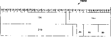
在步骤306中,发射器控制器201的TBQ列队逻辑单元227可使从流队列223出列的FCB排列到TBQ 215中。图10图解说明了驻留于TBQ 215中的FCB的BFCB 1000的字段。BFCB 1000可包括两个条目,每个条目为36位。注意,BFCB 1000可包括任意数目的字段和任意行数,所述字段和行可包括任意数目的二进制位,图10是说明性的。In step 306, TBQ queuing logic 227 of transmitter controller 201 may queue FCBs dequeued from flow queue 223 into TBQ 215. FIG. 10 illustrates the fields of the
驻留于TBQ 215中的FCB的BFCB 1000可包括第一条目中的两个字段,例如下一帧控制缓冲器地址(NFA),与该FCB相关的一个或多个BCB的字节计数(BCNT)长度,以及一个奇偶校验位,和第二条目中的四个字段,例如第一BCB地址(FBA),和与该FCB相关联的第一BCB有关的缓冲器的起始字节位置(SBP),和与该FCB相关联的第一BCB有关的缓冲器的结束字节位置(EBP),帧类型字段(FT),以及一个奇偶校验位。NFA字段可指向TBQ 215中的下一FCB地址,从而允许TBQ 215中FCB的链接。BCNT字段可包括与该FCB相关的一个或多个BCB的字节计数长度。FBA可包括与该FCB相关的第一BCB的地址。SBP可包含和与该FCB相关联的第一BCB有关的缓冲器的起始字节位置。EBP可包括和与该FCB相关联的第一BCB有关的缓冲器的结束字节位置。FT字段可包括该FCB的类型。The
图11图解说明了驻留于TBQ 215中的FCB的FFCB 1100的字段。FFCB可包括一个36位的条目。注意,FFCB 1100可包括任意数目的字段和任意行数,所述字段和行可包括任意数目的二进制位,图11是说明性的。FIG. 11 illustrates the fields of the FFCB 1100 of the FCB residing in the TBQ 215. FFCB may include a 36-bit entry. Note that the FFCB 1100 can include any number of fields and any number of rows that can include any number of bits, FIG. 11 is illustrative.
驻留于TBQ 215中的FCB的FFCB 1100可包括两个字段,例如NFA,与FCB相关的一个或多个BCB的字节计数(BCNT)长度,以及一个奇偶校验位(PTY)。NFA字段可指向下一FCB地址,从而允许TBQ 215中FCB的链接。BCNT字段可包含与该FCB相关的一个或多个BCB的字节计数长度。但是,不访问存储器224的FCBU2 225来取回要保存在驻留于TBQ 215中的FCB的FFCB1100的字段中的信息,因为驻留于TBQ 215中的该FCB的FFCB1100与一帧数据无关。即,驻留于TBQ 215中的该FCB的FFCB1100的字段不重要,于是不必访问与FFCB 1100相关的存储器224的FCBU2 225。The FFCB 1100 of an FCB residing in the TBQ 215 may include two fields, such as NFA, the byte count (BCNT) length of one or more BCBs associated with the FCB, and a parity bit (PTY). The NFA field may point to the next FCB address, allowing chaining of FCBs in TBQ 215. The BCNT field may contain the byte count length of one or more BCBs associated with this FCB. However, the FCBU2 225 of the memory 224 is not accessed to retrieve information to be stored in the fields of the FFCB 1100 of the FCB residing in the TBQ 215 because the FFCB 1100 of the FCB residing in the TBQ 215 is not associated with a frame of data. That is, the fields of the FFCB1 100 of that FCB residing in the TBQ 215 are not important, so it is not necessary to access the FCBU2 225 of the memory 224 associated with the FFCB 1100.
信息可保存在BFCB 1000中,而不是保存在FFCB 1100中,因为TBQ 215由数据流单元110处理,而不是由调度器130处理,下面将进一步说明。于是,驻留于TBQ 215中的该FCB的BFCB 1000的字段可包括有效信息;而驻留于TBQ 215中的该FCB的FFCB1100可不包含有效信息。The information may be stored in the
如上所述,TBQ列队逻辑单元227把从调度器130接收的FCB排列到TBQ 215中。TBQ列队逻辑单元227可向存储器210的FCBU1 209发出一个写入请求,写入TBQ 215中该FCB的BFCB1000的字段,例如NFA、BCNT中的信息。当发射器控制器201从调度器130收到该FCB时,TBQ列队逻辑单元227可从调度器130接收FFCB 900中BCNT字段中的信息的副本。随后,TBQ列队逻辑单元227可被配置成把FFCB 900的BCNT字段中的信息写入BFCB 1000的BCNT字段中。TBQ列队逻辑单元227不发出写入第二条目的字段中的信息的另一写入请求,因为当在流队列223中时,BFCB 800的第二条目的字段中的信息不被更新。从而,TBQ列队逻辑单元227只访问存储器210的FCBU1 209一次,而不是访问两次,从而提高了存储器210的带宽效率。此外,TBQ列队逻辑单元227只向存储器210的FCBU1 209,而不向存储器224的FCBU2 225发出一个写入请求,因为存储器210与数据流单元110相关,而存储器224与调度器130相关。于是,TBQ列队逻辑单元227不访问存储器224的FCBU2 225来写入驻留于TBQ 215中的该FCB的FFCB1100的字段,例如NFA、BCNT中的信息。由于不访问存储器224,因此提高了存储器224的带宽效率。As described above, TBQ queuing logic 227 queues FCBs received from scheduler 130 into TBQ 215. The TBQ queuing logic unit 227 can send a write request to the FCBU1 209 of the memory 210, and write the field of the BFCB1000 of the FCB in the TBQ 215, such as information in NFA and BCNT. When transmitter controller 201 receives the FCB from scheduler 130, TBQ queuing logic 227 may receive from scheduler 130 a copy of the information in the BCNT field in FFCB 900. Subsequently, the TBQ queuing logic unit 227 may be configured to write the information in the BCNT field of the FFCB 900 into the BCNT field of the
在步骤307中,TBQ调度器228可使TBQ 215中的FCB出列,从而如图2的说明中讨论的那样,TBQ调度器228可读取与该FCB相关的帧数据。TBQ调度器228可向存储器210的FCBU1 209发出两个读取请求,读取TBQ 215中该FCB的BFCB 1000的字段中的信息。第一读取请求是读取第一条目的字段,例如NFA、BCNT中的信息。第二读取请求是读取第二条目的字段,例如FBA、FT、SBP、EBP中的信息。TBQ调度器228只可以向存储器210的FCBU1 209,而不向存储器224的FCBU2 225发出这两个读取请求,因为存储器210与数据流单元110相关,而存储器224与调度器130相关。于是,TBQ调度器228不访问存储器224的FCBU2 225来取回用于驻留在TBQ 215中的该FCB的FFCB 1100的字段,例如NFA、BCNT的信息。由于不访问存储器224,因此提高了存储器224的带宽效率。In step 307, TBQ scheduler 228 may dequeue the FCB in TBQ 215 so that, as discussed in the description of FIG. 2 , TBQ scheduler 228 may read frame data associated with that FCB. The TBQ scheduler 228 can send two read requests to the FCBU1 209 of the memory 210 to read the information in the field of the
在步骤308中,一旦与该FCB相关的处理帧数据通过交换机/端口接口单元211被传送给分组交换网络中的交换机(未示出)或者用作到分组交换网络接口的端口(未示出),那么该FCB可排列到FCB判优器206的FCB自由队列222中。FCB判优器206可被配置成从发射器控制器的PCB 224接收与传送的处理帧数据相关的FCB,这里FCB可由PCB 224排列在FCB自由队列222中。In step 308, once the processed frame data associated with the FCB is passed through the switch/port interface unit 211 to a switch (not shown) in the packet switched network or used as a port (not shown) to a packet switched network interface , then the FCB can be arranged in the FCB free queue 222 of the FCB arbiter 206 . The FCB arbiter 206 may be configured to receive an FCB associated with the transmitted processed frame data from the PCB 224 of the transmitter controller, where the FCB may be queued by the PCB 224 in the FCB free queue 222.
如上所述,图4图解说明了驻留在FCB自由队列222中的FCB的BFCB 400的字段。驻留于FCB自由队列222中的该FCB的BFCB 400可包括两个字段,例如NFA(下一FCB地址)、ECC(纠错码)。NFA字段指向下一FCB地址,从而允许FCB自由队列222中FCB的链接。ECC字段可包含纠错码用代码,如美国专利申请序列号09/792533中所述。As mentioned above, FIG. 4 illustrates the fields of the BFCB 400 of the FCBs residing in the FCB free queue 222. The BFCB 400 of the FCB residing in the FCB Free Queue 222 may include two fields such as NFA (Next FCB Address), ECC (Error Correcting Code). The NFA field points to the next FCB address, allowing chaining of FCBs in the FCB free queue 222 . The ECC field may contain a code for an error correction code, as described in US Patent Application Serial No. 09/792533.
如上所述,图5图解说明了驻留在FCB自由队列222中的FCB的FFCB 500的字段。FFCB可包含一个36位的条目。驻留在FCB自由队列222中的该FCB的FFCB 500可包括两个字段,例如NFA,与该FCB相关的一个或多个BCB的字节计数(BCNT)长度,以及一个奇偶校验位(PTY)。NFA字段指向下一FCB地址,从而允许FCB自由队列222中FCB的链接。BCNT字段可包含与该FCB相关的一个或多个BCB的字节计数长度。As mentioned above, FIG. 5 illustrates the fields of the
信息保存在BFCB 400中,而不是保存在FFCB 500中,因为FCB自由队列222由数据流单元110处理,而不是由调度器130处理,下面将进一步说明。于是,驻留在FCB自由队列222中的该FCB的BFCB 400中的字段可包含有效信息;而驻留在FCB自由队列222中的该FCB的FFCB 500中的字段可以包含无效信息。The information is held in the BFCB 400, rather than in the
如上所述,FCB判优器206可被配置成从发射器控制器的PCB224接收与传送的处理帧数据相关的FCB,这里该FCB可由PCB224排列到FCB自由队列222中。PCB 224可向存储器210的FCBU1 209发出一个写入请求,写入用于FCB自由队列222中该FCB的BFCB 400中的字段NFA和ECC的信息。PCB 224只可以向存储器210的FCBU1 209,而不是向存储器224的FCBU2 225发出写入请求,因为存储器210与数据流单元110相关,而存储器224与调度器130相关。于是,PCB 224不访问存储器224的FCBU2225来取回用于驻留在FCB自由队列222中的该FCB的FFCB 500的字段,例如NFA、BCNT的信息。由于不访问存储器224,因此提高了存储器224的带宽效率。As noted above, the FCB arbiter 206 may be configured to receive an FCB associated with transmitted processed frame data from the transmitter controller's PCB 224 , where the FCB may be queued by the PCB 224 into the FCB free queue 222 . The PCB 224 can send a write request to the FCBU1 209 of the memory 210 to write the information for the fields NFA and ECC in the BFCB 400 of the FCB in the FCB free queue 222. PCB 224 can only issue a write request to FCBU1 209 of memory 210, and not to FCBU2 225 of memory 224, because memory 210 is associated with dataflow unit 110 and memory 224 is associated with scheduler 130. Thus, the PCB 224 does not access the FCBU 2225 of the memory 224 to retrieve the fields of the
注意方法300描述了FCB的“生命周期”。还要注意方法300可描述网络处理器100中其它FCB的“生命周期”。另外要指出的是一个或多个不同的FCB可临时同时驻留在每个队列中,例如GQ218、流队列223、TBQ 215、FCB自由队列中。Note that method 300 describes the "lifecycle" of an FCB. Note also that method 300 may describe the "lifecycle" of other FCBs in network processor 100 . It is also to be pointed out that one or more different FCBs may reside temporarily in each queue at the same time, eg GQ 218, flow queue 223, TBQ 215, FCB free queue.
Claims (11)
Applications Claiming Priority (2)
| Application Number | Priority Date | Filing Date | Title |
|---|---|---|---|
| US09/792,494 US7072347B2 (en) | 2001-02-23 | 2001-02-23 | Assignment of packet descriptor field positions in a network processor |
| US09/792,494 | 2001-02-23 |
Publications (2)
| Publication Number | Publication Date |
|---|---|
| CN1528078A true CN1528078A (en) | 2004-09-08 |
| CN100479450C CN100479450C (en) | 2009-04-15 |
Family
ID=25157073
Family Applications (1)
| Application Number | Title | Priority Date | Filing Date |
|---|---|---|---|
| CNB028050126A Expired - Fee Related CN100479450C (en) | 2001-02-23 | 2002-02-20 | Method and system for reducing access to memory |
Country Status (13)
| Country | Link |
|---|---|
| US (1) | US7072347B2 (en) |
| EP (1) | EP1362464B1 (en) |
| JP (1) | JP3880520B2 (en) |
| KR (1) | KR100560277B1 (en) |
| CN (1) | CN100479450C (en) |
| AT (1) | ATE293864T1 (en) |
| AU (1) | AU2002232002A1 (en) |
| CZ (1) | CZ20032126A3 (en) |
| DE (1) | DE60203785T2 (en) |
| ES (1) | ES2237667T3 (en) |
| HU (1) | HUP0303240A3 (en) |
| PL (1) | PL363474A1 (en) |
| WO (1) | WO2002069563A2 (en) |
Families Citing this family (11)
| Publication number | Priority date | Publication date | Assignee | Title |
|---|---|---|---|---|
| US7072347B2 (en) | 2001-02-23 | 2006-07-04 | International Business Machines Corporation | Assignment of packet descriptor field positions in a network processor |
| US7200696B2 (en) * | 2001-04-06 | 2007-04-03 | International Business Machines Corporation | System method structure in network processor that indicates last data buffer of frame packet by last flag bit that is either in first or second position |
| US7099325B1 (en) * | 2001-05-10 | 2006-08-29 | Advanced Micro Devices, Inc. | Alternately accessed parallel lookup tables for locating information in a packet switched network |
| US7535845B2 (en) * | 2004-10-28 | 2009-05-19 | Alcatel Lucent | Intelligent selective flow-based datapath architecture |
| US7376809B2 (en) * | 2005-03-09 | 2008-05-20 | International Business Machines Corporation | Systems and methods for multi-frame control blocks |
| US7466715B2 (en) * | 2005-03-28 | 2008-12-16 | International Business Machines Corporation | Flexible control block format for frame description and management |
| US7787463B2 (en) * | 2006-01-26 | 2010-08-31 | Broadcom Corporation | Content aware apparatus and method |
| DE102008018670A1 (en) | 2008-04-14 | 2009-10-15 | Merck Patent Gmbh | New materials for organic electroluminescent devices |
| US10225196B2 (en) | 2013-02-15 | 2019-03-05 | Nxp Usa, Inc. | Apparatus, system and method for controlling packet data flow |
| CN111654746B (en) | 2020-05-15 | 2022-01-21 | 北京百度网讯科技有限公司 | Video frame insertion method and device, electronic equipment and storage medium |
| CN113835891B (en) * | 2021-09-24 | 2023-05-23 | 哲库科技(北京)有限公司 | Resource allocation method, device, electronic equipment and computer readable storage medium |
Family Cites Families (15)
| Publication number | Priority date | Publication date | Assignee | Title |
|---|---|---|---|---|
| US4817054A (en) | 1985-12-04 | 1989-03-28 | Advanced Micro Devices, Inc. | High speed RAM based data serializers |
| US5136582A (en) | 1990-05-29 | 1992-08-04 | Advanced Micro Devices, Inc. | Memory management system and method for network controller |
| US5983004A (en) | 1991-09-20 | 1999-11-09 | Shaw; Venson M. | Computer, memory, telephone, communications, and transportation system and methods |
| US5604884A (en) | 1993-03-22 | 1997-02-18 | Compaq Computer Corporation | Burst SRAMS for use with a high speed clock |
| EP0622922B1 (en) | 1993-04-29 | 2000-11-29 | International Business Machines Corporation | Method and device of multicasting data in a communications system |
| US5699536A (en) * | 1995-04-13 | 1997-12-16 | International Business Machines Corporation | Computer processing system employing dynamic instruction formatting |
| JPH08328949A (en) | 1995-06-06 | 1996-12-13 | Mitsubishi Electric Corp | Storage device |
| US5898687A (en) * | 1996-07-24 | 1999-04-27 | Cisco Systems, Inc. | Arbitration mechanism for a multicast logic engine of a switching fabric circuit |
| JP3788867B2 (en) | 1997-10-28 | 2006-06-21 | 株式会社東芝 | Semiconductor memory device |
| US6035360A (en) | 1997-10-29 | 2000-03-07 | International Business Machines Corporation | Multi-port SRAM access control using time division multiplexed arbitration |
| JP4182180B2 (en) * | 1999-02-24 | 2008-11-19 | 株式会社日立製作所 | Network relay device and network relay method |
| US6427196B1 (en) * | 1999-08-31 | 2002-07-30 | Intel Corporation | SRAM controller for parallel processor architecture including address and command queue and arbiter |
| US6754216B1 (en) * | 2000-05-08 | 2004-06-22 | Nortel Networks Limited | Method and apparatus for detecting congestion and controlling the transmission of cells across a data packet switch |
| US6751704B2 (en) * | 2000-12-07 | 2004-06-15 | International Business Machines Corporation | Dual-L2 processor subsystem architecture for networking system |
| US7072347B2 (en) | 2001-02-23 | 2006-07-04 | International Business Machines Corporation | Assignment of packet descriptor field positions in a network processor |
-
2001
- 2001-02-23 US US09/792,494 patent/US7072347B2/en not_active Expired - Fee Related
-
2002
- 2002-02-20 AU AU2002232002A patent/AU2002232002A1/en not_active Abandoned
- 2002-02-20 AT AT02712095T patent/ATE293864T1/en not_active IP Right Cessation
- 2002-02-20 CZ CZ20032126A patent/CZ20032126A3/en unknown
- 2002-02-20 JP JP2002568568A patent/JP3880520B2/en not_active Expired - Fee Related
- 2002-02-20 CN CNB028050126A patent/CN100479450C/en not_active Expired - Fee Related
- 2002-02-20 HU HU0303240A patent/HUP0303240A3/en unknown
- 2002-02-20 DE DE60203785T patent/DE60203785T2/en not_active Expired - Lifetime
- 2002-02-20 ES ES02712095T patent/ES2237667T3/en not_active Expired - Lifetime
- 2002-02-20 WO PCT/GB2002/000748 patent/WO2002069563A2/en not_active Ceased
- 2002-02-20 EP EP02712095A patent/EP1362464B1/en not_active Expired - Lifetime
- 2002-02-20 KR KR1020037010704A patent/KR100560277B1/en not_active Expired - Fee Related
- 2002-02-20 PL PL02363474A patent/PL363474A1/en not_active Application Discontinuation
Also Published As
| Publication number | Publication date |
|---|---|
| WO2002069563A2 (en) | 2002-09-06 |
| US7072347B2 (en) | 2006-07-04 |
| DE60203785T2 (en) | 2006-03-09 |
| JP2004530323A (en) | 2004-09-30 |
| KR100560277B1 (en) | 2006-03-10 |
| EP1362464B1 (en) | 2005-04-20 |
| PL363474A1 (en) | 2004-11-15 |
| KR20030076679A (en) | 2003-09-26 |
| DE60203785D1 (en) | 2005-05-25 |
| HUP0303240A3 (en) | 2005-05-30 |
| HUP0303240A2 (en) | 2003-12-29 |
| WO2002069563A3 (en) | 2003-04-17 |
| CZ20032126A3 (en) | 2004-01-14 |
| EP1362464A2 (en) | 2003-11-19 |
| ATE293864T1 (en) | 2005-05-15 |
| JP3880520B2 (en) | 2007-02-14 |
| CN100479450C (en) | 2009-04-15 |
| US20020118690A1 (en) | 2002-08-29 |
| ES2237667T3 (en) | 2005-08-01 |
| AU2002232002A1 (en) | 2002-09-12 |
Similar Documents
| Publication | Publication Date | Title |
|---|---|---|
| US12341686B2 (en) | System and method for facilitating efficient utilization of an output buffer in a network interface controller (NIC) | |
| CN112084136B (en) | Queue cache management method, system, storage medium, computer device and application | |
| US6857030B2 (en) | Methods, system and article of manufacture for pre-fetching descriptors | |
| JP5640234B2 (en) | Layer 2 packet aggregation and fragmentation in managed networks | |
| US7852867B2 (en) | Integrated memory for storing egressing packet data, replay data and to-be egressed data | |
| TW202230112A (en) | Plane-based queue configuration for aipr-enabled drives | |
| CN1545658A (en) | Switch fabric with dual-port memory emulation configuration | |
| CN1643872A (en) | Caching streaming data | |
| US7447230B2 (en) | System for protocol processing engine | |
| CN1528078A (en) | Allocation of Packet Descriptor Field Locations in Network Processors | |
| US7552232B2 (en) | Speculative method and system for rapid data communications | |
| CN1543733A (en) | In-Band Message Synchronization for Distributed Shared Memory Packet Switches | |
| CN1502198A (en) | Link frame data by inserting qualifiers into control blocks | |
| US9804959B2 (en) | In-flight packet processing | |
| US20030065832A1 (en) | Enhanced power reduction capabilities for streaming direct memory access engine | |
| US9137167B2 (en) | Host ethernet adapter frame forwarding | |
| EP3896881B1 (en) | Harq data storage management method and device and harq data buffer | |
| CN1965550A (en) | Method and apparatus for processing a complete burst of data | |
| CN101043437A (en) | Method and apparatus for transmitting quickly operation, management and maintenance cell | |
| US9559988B2 (en) | PPI allocation request and response for accessing a memory system |
Legal Events
| Date | Code | Title | Description |
|---|---|---|---|
| C06 | Publication | ||
| PB01 | Publication | ||
| C10 | Entry into substantive examination | ||
| SE01 | Entry into force of request for substantive examination | ||
| C14 | Grant of patent or utility model | ||
| GR01 | Patent grant | ||
| CF01 | Termination of patent right due to non-payment of annual fee |
Granted publication date: 20090415 Termination date: 20200220 |
|
| CF01 | Termination of patent right due to non-payment of annual fee |