The display device of band camera head
Technical field
The present invention relates to display device, wherein have the picture pick-up device that forms as one with more slim display device such as organic EL, liquid crystal, plasma mode with camera head.In more detail, the display device that relates to the band camera head that is suitable in the real time bidirectional communication such as band videophone etc. etc.
Background technology
In recent years, along with the communication network alarming development, real time bidirectional communications such as videophone have become possibility.Videophone is by subject being looked like be transformed into the image unit of electrical picture signal and electrical picture signal being transformed into light signal and the display unit that shows constitutes.The user of videophone carries out session while the face of seeing the other side who mirrors on the picture of display unit, utilizes image unit shooting user's face simultaneously and deliver to the other side's side after being transformed into electric signal.But, in the equipment that in two-way communications such as existing videophone, uses, be arranged on image unit near the display unit or as another independent device setting, the result is to take the receipts words people who is seeing display unit from oblique direction.Therefore, the sight line of the other side's who mirrors on display unit face is towards other place, and talk also seems dumb mutually, compares with the situation of talking in the opposite, exists the problem of feeling not harmony.In addition, must make camera head and display device respectively and assemble or must make device separately again, exist the problem that manufacturing cost improves.
Therefore, open in the flat 10-70713 communique, disclose the structure that in the viewing area of display unit, is provided with image unit the spy.Figure 33,34,35 is for illustrating the figure of this conventional example, and Figure 33 illustrates whole oblique view, and Figure 34 illustrates the enlarged drawing of the A-A ' section among Figure 33, and Figure 35 illustrates the shooting principle of subject.Shown in Figure 33,34, transmission-type camera head integrated display apparatus is made of display device 1 and transmission-type camera head 2.Display device 1 is the liquid crystal indicator of transmission-type, is thrown light on from behind by illumination light 5.Transmission-type camera head 2 is made of the lenticule 4 that is arranged in cancellate window portion 3 and be configured on the intersection point of window and window.By irradiates light 5 images irradiation, display device 1, the window portion 3 by transmission-type camera head 2 is observed.And, be provided with the lenticule 4 of transmission-type camera head and photodiode 26 etc. on the TFT10 top of display device 1.Therefore, can make a video recording simultaneously and show.And, become the structure of utilizing 1 lenticule 4 and photodiode 26 to obtain 1 image pickup signal.
Below, the shooting principle of the subject of such compound eye imaging apparatus is described with Figure 35.Figure 35 is the vertical cross section of transmission-type camera head 2, on transparent glass substrate 21, dispose photodiode 26 to form photodiode array 38 with constant interval, each photodiode 26 is covered by light shield layer 30 respectively, has pin hole 31 on light shield layer 30.The microlens array 35 that configuration is made of the lenticule 4 corresponding to each photodiode 26 before photodiode array 38.Subject 39 is positioned at the place ahead of microlens array 35, outer light 37 from subject 39 is shown incides situation on each photodiode 26.At this, the distance that microlens array 35 is configured in light shield layer 30 is on the position of focal distance f of lenticule 4.Therefore, have only the light 37 on the specific direction that links pin hole 31 and the optical centre of lenticule 4 can incide photodiode 26.And, if make outer light 37 all become light parallel to each other, just can take the subject 39 that is positioned at transmission-type camera head 2 the place aheads into about being the size of camera head 2 by lenticule battle array 35.
In structure as described above, can take the former state of seeing display unit, and, can make the other side who shows on sight line and the display unit consistent.In addition, by in the display unit front slim image unit being set, whole device does not maximize yet.
But, in above-mentioned conventional example, exist following problem.
(1) pixel count of the pixel count of photographic images and display device is roughly equal, can not carry out the above high pixelation of display pixel number.
(2) owing to form the low photodiode of fabrication yield on the such big space of a whole page substrate size of display device, so the number that can form on 1 substrate is few, and cost improves.
(3) in order to form window portion photoelectric conversion department is set discretely, has produced Moire fringe (ripple).
Summary of the invention
Therefore, the present invention proposes just in view of the above problems, and its purpose is, in the display device of band camera head, can make the sight line unanimity with simple structure, meanwhile, realizes high pixelation, cost degradation, slimming.
And then, accomplish the high-definition image that can obtain not having Moire fringe.
Achieve the goal in order to address the above problem, provide a kind of display device according to a first aspect of the present invention with camera head, it is characterized in that, comprising: display unit, it has a plurality of display pixels and is configured in shading member between each display pixels of this a plurality of display pixels; And the image unit that is configured in this display unit back, above-mentioned shading member has the peristome that is used for light is directed on the above-mentioned image unit on the part, and above-mentioned image unit has image-generating unit on the position corresponding to above-mentioned peristome.
In addition, provide a kind of display device, it is characterized in that, comprising with camera head according to a second aspect of the present invention: display unit, it has a plurality of display pixels and is configured in shading member between each display pixels of this a plurality of display pixels; And a plurality of image units that are configured in this display unit back, above-mentioned shading member has a plurality of peristomes that are used for light is directed on the above-mentioned image unit on the part, set above-mentioned a plurality of peristome with the integral multiple spacing of above-mentioned display pixel.
From the following description of being done in conjunction with the accompanying drawings, other features and advantages of the present invention will be more obvious, and in whole accompanying drawings, similarly label is represented identical or similar parts.
Description of drawings
Fig. 1 is the part sectioned view of the organic EL display of simple matrix mode.
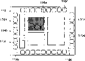
Fig. 2 is the planimetric map of the organic EL display seen from anode-side.
Fig. 3 is the planimetric map of the organic EL display seen from cathode side.
Fig. 4 is the summary section after the part of the display device of the band camera head in the 1st embodiment is amplified.
Fig. 5 is the planimetric map of the display unit from Fig. 4 that anode-side is seen.
Fig. 6 is the planimetric map of the display unit from Fig. 4 that cathode side is seen.
Fig. 7 is the planimetric map of the imaging apparatus seen from the lens section side.
Fig. 8 sees from oblique upper, the oblique view of circuit board and the articulate state of imaging apparatus.
Fig. 9 is the figure of the optical system naive modelization of the image unit shown in Fig. 4.
Figure 10 is the outward appearance oblique view of the display device of band camera head.
Figure 11 is the block diagram that the system that realizes the real time bidirectional Image Communication is shown.
Figure 12 is the block diagram that illustrates in greater detail the electric structure of the display device of being with camera head.
Figure 13 is the skeleton diagram that is illustrated in the state of display application software on the display screen.
Figure 14 is the process flow diagram of the work when the application software starting is shown.
Figure 15 is the planimetric map of the display unit from the 2nd embodiment that anode-side is seen.
Figure 16 is the planimetric map of the display unit from the 2nd embodiment that cathode side is seen.
Figure 17 is the summary section after the part of the display device of the band camera head in the 3rd embodiment is amplified.
Figure 18 is the planimetric map of the display unit from Figure 17 that anode-side is seen.
Figure 19 is the planimetric map of the display unit from Figure 17 that cathode side is seen.
Figure 20 is the planimetric map of the imaging apparatus from the 3rd embodiment that the display unit side is seen.
Figure 21 is the planimetric map of the pad seen from the display unit side.
Figure 22 is the figure of naive modelization around the optical system of Figure 16.
Figure 23 is the summary section after the part of the display device of the band camera head in the 4th embodiment is amplified.
Figure 24 is the planimetric map of the main member from Figure 23 that top surface side is seen.
Figure 25 is the planimetric map of black matrix.
Figure 26 is the block diagram that the electrical structure of display unit is shown.
Figure 27 is the figure that the equivalent circuit of display pixel is shown.
Figure 28 is the summary section after the part of the display device of the band camera head in the 5th embodiment is amplified.
Figure 29 is the planimetric map of display screen that the display device of the band camera head with a plurality of image units is shown.
Figure 30 is the skeleton diagram that is illustrated in the state of display application software on the display screen.
The planimetric map of the display screen among Figure 29 that Figure 31 sees for side from the side.
Figure 32 is the planimetric map of the display screen from Figure 29 that end face or bottom surface side are seen.
Figure 33 is the whole oblique view of the display device of the band camera head in the conventional example.
Figure 34 is the enlarged drawing on the A-A ' section among Figure 33.
Figure 35 is the figure that the shooting principle of the subject in the conventional example is shown.
Embodiment
Below, the preferred embodiment of the present invention is described.
The summary of embodiment of the present invention at first, is described.
The display device of the band camera head of embodiment is characterized in that, comprising: display unit, and it has a plurality of display pixels and is configured in shading member between each display pixels of this a plurality of display pixels; And the image unit that is configured in this display unit back, above-mentioned shading member has the peristome that is used for light is directed on the above-mentioned image unit on the part, and above-mentioned image unit has image-generating unit on the position corresponding to above-mentioned peristome.
In addition, the display device of the band camera head of another embodiment is characterized in that, comprising: display unit, and it has a plurality of display pixels and is configured in shading member between each display pixels of this a plurality of display pixels; And a plurality of image units that are configured in this display unit back, above-mentioned shading member has a plurality of peristomes that are used for light is directed on the above-mentioned image unit on the part, set above-mentioned a plurality of peristome with the integral multiple spacing of above-mentioned display pixel.
In addition, in the display device of the band camera head of this embodiment, it is characterized in that near the part of the above-mentioned display pixel the above-mentioned peristome has breach.
In addition, in the display device of the band camera head of this embodiment, it is characterized in that above-mentioned a plurality of image units carry out pixel for the subject of predetermined distance to be departed from (pixel-shift) and take.
Below, with reference to accompanying drawing, explain embodiments of the present invention.
(the 1st embodiment)
The 1st embodiment is to have used the example of organic EL (electroluminescence) element as display unit.Organic EL is the element of emissive type, has under the situation of display device being used for: (1) luminescence efficiency height; (2) driving voltage is low; (3), can show various looks (green, red, blue, Huang etc.) by selecting luminescent material; (4) do not need to carry on the back the irradiation source; (5) be that face is luminous, no viewing angle dependence; And good feature such as (6) slim, in light weight.Therefore, in recent years, instead the display device of CRT or LCD uses the display device of organic EL to come into one's own.Below, before the explanation present embodiment, at first, organic EL display is described.
In the dot matrix organic EL display that shows with the point (point) that is configured to matrix, simple matrix mode and active matrix mode are arranged.
The simple matrix mode is the mode that synchronously directly drives for the organic EL that is configured to each pixel of matrix at display screen with sweep signal from outside, only constitutes the display screen of display device with organic EL.Therefore, exist the driving time (energy rate) that when the number of scanning lines increases, is assigned to 1 pixel and reduce, the problem that contrast reduces, still, having can simplified manufacturing technique, and advantage that can cost degradation.
Fig. 1 to Fig. 3 illustrates the organic EL display of simple matrix mode.Fig. 1 is the part sectioned view of the organic EL display 101 of simple matrix mode.
On the transparent insulation substrate 102 that constitutes by glass or synthetic resin etc., a plurality of anodes the 103, the 1st hole transporting layer the 104, the 2nd hole transporting layer 105 that constitutes by ITO transparency electrodes such as (indium tin oxides), luminescent layer 106, electron supplying layer 107, by a plurality of negative electrodes 108 that the magnesium indium alloy constitutes, form with this sequential cascade.Like this, each layer 104~107 is made of organic compound, and each layer 104~107 constitutes organic EL 109 with anode 103 and negative electrode 108 by this.
In addition, on the transparent insulation substrate of exposing between each anode 103 102, form as the black matrix 110 shading member, that constitute by photomask with insulativity.That is, black matrix 110 forms with the state that is embedded between each anode 103.Material as black matrix 110, coating dielectric film (silicon resin film, polyimide resin film, SOG (in spin-on-glass) film etc.) that comprises the particulate (carbon black etc.) with light-proofness or the polymeric membrane with light-proofness etc. are arranged, so long as antianode 103 does not cause the material of bad influence, which kind of material can.
In organic EL 109, from anode 103 injected holes with combine again in the inside of luminescent layer 106 from negative electrode 108 injected electrons, excite the organic molecule that forms luminescent layer 106 and produce exciton.This exciton is luminous from luminescent layer 106 in the process of radiation deactivation, and shown in arrow γ, this light passes through transparent insulation substrate 102 to external emission from transparent anode 103.
At this, each hole transporting layer 104,105 has to be made the function that the hole injects from anode 103 easily and stops from the function of negative electrode 108 injected electrons.In addition, electron supplying layer 107 has the function that electronics is injected from negative electrode 108 easily.
According to the organic EL display 101 of such formation, can obtain the organic EL 109 of the high bill coloured light of luminescence efficiency, the brightness of organic EL display 101 is improved.
And, for the organic EL display 101 of realizing full color, 5 kinds of following methods have been proposed.(1) the organic EL of the coloured light that turns white and the combination of RGB color filter.(2) utilize CCM (medium are changed in variable color) color conversion layer that the organic EL of sending out B (indigo plant) coloured light is transformed into and send out rgb light.(3) use the protection mask to form each organic layer of RGB selectively.(4) stacked in vertical direction each organic EL of RGB makes each EL element luminous independently.(5) utilize ink jet printing separately to apply each organic layer of RGB, make it to send out rgb light.
Fig. 2 is the planimetric map of the organic EL display 101 seen from anode 103 sides.Anode 103 and negative electrode 108 other member have in addition been omitted among Fig. 2.The configuration abreast respectively of each anode 103, each negative electrode 108 is configuration abreast respectively also.And be configured to make each anode 103 and each negative electrode 108 to distinguish quadratures.
In organic EL 109, each anode 103 that intersects (103a~103c) and each negative electrode 108 (zone of clamping respectively between the 108a~108c), promptly among the figure with the zone shown in the oblique line portion in each light-emitting zone A of formation, this light-emitting zone A is luminous by above-mentioned effect.That is, each the light-emitting zone A that is configured to matrix becomes each display pixel of organic EL display 101.
In the simple matrix mode, the positive side of driving power is connected with the anode 103 corresponding with being controlled so as to luminous light-emitting zone A, the minus side of driving power is connected with the negative electrode 108 corresponding with this light-emitting zone A, to this anode 103 and negative electrode 108 energisings.
For example, wanting to make under the luminous situation of light-emitting zone A on the point of crossing that is positioned at anode 103 and negative electrode 108a, as side just, 108a switches on as minus side negative electrode anode 103.So forward current flows shown in arrow α.
The organic EL display 101 of Fig. 3 for seeing from negative electrode 108 sides omitted black matrix 110 and anode 103 other member in addition.And because anode 103a~103c is arranged on the downside of black matrix 110, Gu Tuzhong is shown in broken lines.On black matrix 110, the zone corresponding with light-emitting zone A among Fig. 2 forms as open area B.And, constitute each light-emitting zone A regional shading in addition, to have played the effect that prevents that light from leaking.
Like this, because the organic EL display of present embodiment has black matrix 110, so the optical crosstalk that the light scattering that the structure of optical crosstalk that the very difficult leakage current characteristic that produces EL element causes or EL element causes causes.Therefore, because the contrast of organic EL display 101 becomes good and resolution improves, so can access high-precision thin image.And, under the situation of the organic EL display that is applied to full color, can obtain the few bright-coloured image of look " hangover ".
Be the structure of organic EL display above.In the present embodiment, such organic EL display is used as display unit.
Fig. 4 is the summary section after the part of the display device of the band camera head in the 1st embodiment is amplified.
Among Fig. 4,111 display device for the band camera head that constitutes by image unit 112 and display unit 113.Use the organic EL display 101 of Fig. 1 as display unit 113, equally, on the transparent insulation substrate 102 that constitutes by glass or synthetic resin etc., form a plurality of anodes 103 that constitute by ITO transparency electrodes such as (indium tin oxides), between each anode 103, form black matrix 110.114 is at anode 103, the black stacked organic layer of matrix 110 upper surfaces, is made of the 1st hole transporting layer the 104, the 2nd hole transporting layer 105, luminescent layer 106, electron supplying layer 107 among Fig. 1.And, a plurality of negative electrodes 108 that stacked formation is made of the magnesium indium alloy on the upper surface of organic layer 114.More than be the structure of display unit 113, the same with the organic EL display 101 that uses Fig. 1 to Fig. 3 to illustrate.
Secondly, the structure of image unit 112 is described.The stacked duplicating layer 115 that has lens section 115a integratedly on the upper surface of negative electrode 108.Duplicating layer 115 general use uv-hardening resins etc. are shaped by metal pattern and make, and make face, sphere and the aspherical shape of high precision such as imaging len even the lens arra of dense arrangement, can easily realize.Have again, as the general preferred use acrylic resin of imaging len.
But, in organic EL 109, electrode because of the oxygen of minute quantity and moisture with regard to the oxidized not illuminating part that is called the oxidation blackspot that forms easily, enlarge to come as time passes and become non-luminous phenomenon, become problem.In the present embodiment, be the structure that the organic EL 109 that is made of anode 103, organic layer 114, negative electrode 108 is sealed fully with transparent insulation substrate 102 and duplicating layer 115.Therefore, duplicating layer 115 not only in order to form lens section 115a, also plays the effect of sealing.Have again, because duplicating layer 115 is resins, so for complete sealed external api request 115 has to a certain degree thickness, but, under the situation that only can not seal fully with duplicating layer 115, can on duplicating layer 115, apply, beyond metal film coating lens section 115a, seal whole device.
Turn back to Fig. 4, the imaging len of lens section 115a for constituting by aspherical shape, L1 illustrates the optical axis of lens section 115a.And, on the black matrix 110 that intersects with optical axis L 1, be provided with peristome 110a.This peristome 110a plays the effect of the opening diaphragm of lens section 115a.
By such work, the light by transparent insulation substrate 102, peristome 110a, organic layer 114 utilizes lens section 115a imaging.Have, organic layer 114 is a film again, the visible rays transmission many, get final product but peristome is set again when not being such on organic layer 114.In the present embodiment, in order to eliminate the trouble of manufacturing process as far as possible, make the structure that peristome is not set on organic layer 114.
Secondly, the planimetric map of the display unit 113 of Fig. 5 from Fig. 4 that anode 103 sides are seen.Among Fig. 5, anode 103 and negative electrode 108 other member have in addition been omitted.Among the figure, the circle that is shown in broken lines is corresponding to lens section 115a, is that the center forms this circle with optical axis L 1 on the zone of clamping with anode 103a, 103b, negative electrode 108a, 108b.And the overlapping zone A of oblique line portion of anode 103a~103c and negative electrode 108a~108c is used as light-emitting zone.That is, each the light-emitting zone A that is configured to matrix becomes each display pixel of display unit 113.
Equally, Fig. 6 is the planimetric map of the display unit 113 from Fig. 4 that negative electrode 108 sides are seen.Have again, among Fig. 6, omitted anode 103 and black matrix 110 other member in addition.The zone corresponding to light-emitting zone A of black matrix 110 forms as open area B, but other zone forms shading.And, on corresponding to the position lens section 115a that is shown in broken lines, that with optical axis L 1 be the center, formed circular peristome 110a.At this, as can be known, Fig. 4 is the sectional view of the horizontal direction among Fig. 5 and Fig. 6.
Like this, on locational black matrix 110, utilize the unwanted zone in demonstration between each light-emitting zone A to form circular peristome 110 corresponding to lens section 105a.Therefore, display quality is not reduced.
Negative electrode 108 is owing to be metal film, so transmitted light not.In the present embodiment, because lens section 115a and peristome 110a are arranged on the zone that does not have metal film between negative electrode 108a, 108b, so need on metal film, not form peristome, but, in this zone, have under the situation of light-proofness members such as negative electrode, certainly peristome must be set suitably.In the present embodiment, for making the optical axis L 1 of lens section 115a, the trouble of eliminating technology is arranged in the zone that does not have metal film.And then, because peristome 110a is circular, so, can also increase the diameter of peristome 110a more by optical axis L 1 being set in like this center of 4 display pixels.Therefore, can improve the design freedom of F numerical value.
Optical property as image unit 112 sides, the light of worry by near the open area B for example peristome 110a except that the peristome 110a shown in Fig. 6 enters and utilizes in the subject picture that lens section 115a forms, and makes the picture mis-behave as ghost image, flicker.In the present embodiment, make the structure that such light is covered fully owing on the B of open area, exist the negative electrode 108 that constitutes by metal film, but, for the light that utilizes organic layer 114 emissions is fetched into the display surface side expeditiously, form negative electrode 108 with the high metal film of reflectivity mostly, this also has the possibility that causes ghost image, flicker.In the case, as long as form black matrix 110 thicklyer, so that fully separately organic layer 114 gets final product.And then, in duplicating layer 115 sides of negative electrode 108, and near image unit 112 formation antiradar reflectivity film, do one's utmost to eliminate the light reflection on duplicating layer 115 sides of negative electrode 108.Have again, because the light quantity of duplicating layer 115 sides of negative electrode 108 and demonstration is irrelevant, so even make such structure, also no problem.
Turn back to Fig. 4, the imaging apparatus encapsulation unit 119 being made of imaging apparatus 116, circuit board 117, cover glass 118 is arranged on by bond layer 120 near the image space of lens section 115a.And, apply by multilayer film in the plane of incidence side of cover glass 118 and to form IR-cut layer 121 and stop the infrared light that shooting is caused the ring influence.
Fig. 7 is the planimetric map of the imaging apparatus 116 seen from lens section 115a side.On imaging apparatus 116, form a plurality of light receiving pixel 116a with clathrate, utilize these a plurality of light receiving pixel 116a that the subject that utilizes lens section 115a imaging is looked like to carry out light-to-current inversion.And per 1 pixel has color filter (not shown), lenticule (not shown) respectively in light receiving pixel 116a, arranges by using for example known Bayer (Bayer) as the arrangement of color filter, can take the photograph coloured image.And the 116b peripheral circuit on the chip that generating unit, A/D transformation component etc. constitute of serving as reasons regularly is provided with integratedly with light receiving pixel 116a on imaging apparatus 116.And then, on these peripheries, with circular formation electrode welding zone 116c.On electrode welding zone 116c, form au bump (not shown),, au bump is electrically connected with the electrode part (not shown) of circuit board 117 by anisotropic conductive paste or heat and ultrasound wave joint.And, can read image pickup signal by circuit board 117.
Fig. 8 sees from oblique upper, the oblique view of circuit board 117 with imaging apparatus 116 articulate states.Peristome 117a is set on circuit board 117, exposes light receiving pixel 116a so that can look like to carry out light-to-current inversion to subject.And, this circuit board 117, with imaging apparatus 116 opposed sides, by peristome 117a configuration cover glass 118.Therefore, exist the micro-air layer, can bring into play the optical effect of the lenticule (not shown) that on light receiving pixel 116a, forms at the light receiving pixel 116a and 118 of the cover glasses of imaging apparatus 116.Have again, on the interface of each member, form the adhesive sealant layer of ultraviolet ray and thermmohardening type, when keeping physical strength, constitute in the lump the hermetically-sealed construction of the sensitive surface of imaging apparatus 116 and extraneous air partition with anisotropic conductive paste.
But, the detailed structure of such imaging apparatus encapsulation unit 119 is disclosed in No. 3207319 communique of patent, use this imaging apparatus encapsulation in the present embodiment.As the feature of such encapsulation, be the light path of image pickup optical system because the circuit board 117 that is used for taking out image pickup signal is arranged between light receiving pixel 116a and the lens section 115a, so can realize more slim camera head.
And imaging apparatus encapsulation unit 119 is passing through position adjustment such as inclination, rotation so that the subject picture that utilizes lens section 115a to form after the imaging, utilizes bond layer 120 to be fixed on the sensitive surface of imaging apparatus 116.
As mentioned above, constitute image unit 112 with peristome 110a, lens section 115a, imaging apparatus encapsulation unit 119.And, be illustrated in the light of imaging on the edge, light area of imaging apparatus 106 among the figure with the line shown in C, the D, can be to the subject shooting at regulation visual angle.
As an example, the size around the image unit 112 is calculated in examination.Fig. 9 uses this figure to calculate for the figure of the optical system naive modelization of the image unit shown in Fig. 4 112.
Among Fig. 9,102 ' corresponding to transparent insulation substrate 102, and 105 ' corresponding to duplicating layer 115.And the 115a ' of spherical lens portion is corresponding to lens section 115a, for make calculate simple, establish sphere and be on 102 ' and 115 ' interface, have central point E, radius is the sphere of r.In addition, be the aperture of the diaphragm that is equivalent to the 115a ' of spherical lens portion of peristome 110a at d, establish 102 ', 115 ' refractive index and be n without exception.And then H is the Diagonal Dimension in the zone of the light receiving pixel 116a of formation imaging apparatus 116, and light C ', D ' are the light that also passes through central point E in the imaging of the end of H.Therefore, light C ', D ' be only by 102 ' plane of incidence refraction, can't help other boundary surface refraction.
Like this, the power by weakening the plane of incidence, strengthen the power of outgoing plane, promptly by in the optical system of plano-convex structure at the radius r center configuration diaphragm of sphere, can reduce curvature of the image.Have again, in practice, by sphere is made aspheric surface, various aberrations such as bending with sizing aberration, chromatic aberation better.
θ is the angle of light C ', D ', promptly takes the visual angle, and θ ' is by the shooting visual angle after the optical system refraction.
Now, be 320 * 240 QVGA size for example at the pixel count of imaging apparatus 116, when pel spacing was 0.003mm, Diagonal Dimension H was as follows.
H=0.003×(320
2+240
2)
1/2=1.20mm ……(1)
Floor angle θ can at random set, but in the present embodiment because display device and user's distance is nearer to a certain extent, so hope is set at wide-angle, as if θ=60 °, refractive index n=1.5 o'clock, θ ' is as follows according to Snell's law.
θ’=2×asin(sin(θ/2)/n)=38.94° ……(2)
Therefore, as follows from central point E to H apart from l.
l=(H/2)/tan(θ’/2)=1.70mm ……(3)
And, because the thickness of transparent insulation substrate 102 is generally 0.7mm, when being the wafer standard size, imaging apparatus 116 also is about 0.7mm, so integral thickness is about 3.10mm.
On the other hand, when the focal length of the 115a ' of spherical lens portion was f, subject position and focal length were in a ratio of fully far, roughly can be approximately infinity, and under the situation of refractive index n=1.5, since f=2r, l=3r, so can be by f=1.13mm, r=0.57mm calculates.And, when the F numerical value of the 115a ' of spherical lens portion is F8.0, aperture of the diaphragm d=0.14mm.
Have again, in the naive model of Fig. 9, omitted anode 103, organic layer 114, negative electrode 108, describe.This be because, these the layer be film, gross thickness is about several microns, considers its omission is also harmless.In addition, lens section 115a is considered as the spherical lens of having ignored various aberrations, also no problem when calculating approximate dimension like this.
On the other hand, when the diagonal line of the display screen of display unit 113 was 15 inches, horizontal length was 12 inches (304.8mm), and vertical length is 9 inches (228.6mm).And when the display pixel number was the VGA correspondence display device of 640 * 480 pixels, the level of display pixel and vertical interval all were 0.476mm.Aperture opening ratio at display pixel is 60% o'clock, and the width of black matrix 110 can followingly calculate.
1 edge lengths of opening: (0.476
2* 0.6)
1/2=0.369mm ... (4)
Black matrix width between each display pixel: 0.476-0.369=0.107mm ... the Diagonal Dimension of the black matrix between (5) 4 display pixels:
And this black diagonal of a matrix size is the size F among Fig. 6, is very possible for forming aperture of the diaphragm 0.14mm.Have, when doing one's utmost to shrink the aperture of the diaphragm, the contrast of high frequency band reduces because of diffractive effect again.This is because the intensity of the diffraction fringe that the Zhou Bianbo that sends from the diaphragm edge of opening causes increases.In order to reduce diffraction fringe, be transparent and along with the color filter that increases towards peripheral concentration gets final product at the additional central portion of peristome.This method is called apodization, can form this color filter by films such as evaporation or sputter tophet, chrome-nickel alloy, chromium.
As mentioned above, by on black matrix 110, forming the hole of aperture 0.14mm, can realize that thickness is the display device of the super thin tape camera head of 3.10mm.
Figure 10 is the outward appearance oblique view of the display device 111 of such band camera head.
130 is the display screen of display unit 113, the visual information that shows on this display screen 130 of user.And, image unit 112 is imbedded shown in dashed lines among the figure near the central authorities of display screen 130.Having, because the peristome 110a of image unit 112 is small, is difficult so look from display screen 130 sidelong glance again, has also omitted among the figure.131 baskets for the display device 111 of the band camera head that supports present embodiment.
Figure 11 is the block diagram that display device 111 that the band camera head that utilizes present embodiment is shown realizes the system of real time bidirectional Image Communications.In the present embodiment, illustrate the display device 111 of band camera head is connected the example of realizing by utilizing signal conditioning package to control with PC signal conditioning packages 141 such as (personal computers).
140 for comprising the information terminal of the display device 111 of being with camera head, is made of display device 111 and the signal conditioning package 141 of being with camera head.
Signal conditioning package 141 is known structure, comprises high capacity mediums 144 such as central arithmetic processing section 142, storer 143, for example hard disk.OS (operating system) is stored in the high capacity medium 144, utilizes programmed control to carry out the starting of signal conditioning package 141.In addition, also be stored in the high capacity medium 144 with the application software of the various work controls of the display device 111 of camera head, the beginning of making a video recording under the control of OS, communicating by letter Control work such as begins.In addition, comprise microphone 145, the loudspeaker 146 that is used to carry out audio communication in the signal conditioning package 141.And then, though not shown, also be connected with known mouse, the keyboard of management of user's interface.
Signal conditioning package 141 generally is connected with network 147 by telephone line or LAN circuit.And, be connected with many station informations terminal 140a, 140b, 140c by this network 147.
Utilize said structure, realize the real time bidirectional Image Communication.
Figure 12 is the block diagram that illustrates in greater detail the electric structure of the display device 111 of being with camera head.
Comprise display unit 113 and image unit 112 in the display device 111 of band camera head.
At first, in display unit 113,150 for having the display part of a plurality of display pixels that are made of the light-emitting zone A among Fig. 4, and 151 be the demonstration IF portion that signal conditioning package 141 external connection apparatus such as grade from Figure 11 accept to show the usefulness signal.And 152 for driving the display driver circuit of a plurality of display pixels with signal based on the demonstration of sending here with IF portion 151 by demonstration.
Secondly, in image unit 112, have the light area 153 that is made of a plurality of light receiving pixel 116a shown in Fig. 7 in imaging apparatus 116, TG (timing generator) portion 155 that the simulating signal of utilizing each light receiving pixel 116a to carry out light-to-current inversion is transformed into the A/D transformation component 154 of digital signal and various timing signals is delivered to A/D transformation component 154 forms as one with imaging apparatus 116.The 156th, the picture signal that is transformed into digital signal with the A/D transformation component is carried out various Flame Image Process such as automatic exposure, Gamma correction, white balance adjustment, filtering operation, be created on the image processing part of the picture format that can launch on the signal conditioning package 141.And, the 157th, image is delivered to signal conditioning package 141, accept the shooting IF portion of shooting timing signal from signal processing apparatus 141.
At this, constitute display unit 113 and be connected with signal conditioning package 141 by oneself respectively with image unit 112.This is because the connecting interface of display unit and signal conditioning package is determined by standard specification, just becomes specification alone when adding the specification that connects image pickup signal, and lacks versatility.Have, the connected mode with versatility that the connection of image unit 112 uses animated image such as known USB, IEEE1394 connection to be suitable in transmitting gets final product again.
Figure 13 is the skeleton diagram that shows the state of the application software of carrying out two-way communication on the display screen 130 that is illustrated among Figure 10.Have, as mentioned above, this application software stores is started by user's operation in the high capacity medium 144 of signal conditioning package 141 again.
Among the figure, 160 is application window, comprising: a plurality of instruction input parts 161 that get up side by side of order button that the user carried out the setting or the operation of various functions; The image display window 162 (figure bend portion) that shows image that utilizes image unit 112 shootings or the image that sends over communicating by letter; And in the button that instruction is had in the input part 161 with shooting or the relevant a plurality of order buttons of communicating by letter are selected gets up side by side so that the user carries out the shooting and the communication instruction input part 163 of transient operation easily.Have again,, utilize known mouse and keyboard to carry out about user's instruction input part 161 and setting and the operation in shooting and the communication instruction input part 163.
164 is the image unit position mark that the location of image unit 112 is shown.This image unit position mark can utilize instruction input part 161 and shooting and communication instruction input part 163 at random to be set at demonstration/do not show.Such label handlebar user make a video recording or preferably watch display screen 130 during two-way communication attentively which place notify user's effect, as present embodiment, the aperture of peristome 110 is very small, and under by visual situation about can not roughly differentiate, this mark is resultful.
And then, in application window 160, have own image display window 165, make the user can confirm oneself what to look.
Figure 14 is the process flow diagram of the work when application software as described above starting is shown.
At first, in STEP1401,, under the OS of signal conditioning package 141 control, start application software by the operation of mouse etc.
Secondly, in STEP 1402, shows signal is delivered to display unit 113 from signal conditioning package 141, display application window 160 on display screen 130.
Secondly, in STEP 1403, do you differentiate image unit position mark show label and have become ON? so-called image unit position mark show label refers to, the setting of the demonstration of the image unit position mark 164 that can at random set by above-mentioned user/do not show, show label ON.And, constitute, when finishing, application software stores the state of this sign, when starting, it is read next time.
Secondly, be under the situation of ON at image unit position mark show label, enter STEP1404, display message is delivered to display unit 113 from signal conditioning package 141, the foremost in display screen 130 shows image unit position mark 164.Therefore, even started other application software, under the situation that the application software of present embodiment is just being used, also show image unit position mark 164 in the foremost of application window 160, therefore, the user can easily discern the location of image unit 112.
On the other hand, not under the situation of ON at image unit position mark sign, do not show image unit position mark 164, a display application window 160.
Be the work when using starting above.And, because the work of relevant shooting or communication is known, the Therefore, omited its explanation.
Utilize structure as described above, realize the real time bidirectional Image Communication.And, has the image unit 112 under the state that does not stretch out from display device 113, and then, the peristome 110a of image unit 112 also is set under the situation of not losing display pixel, the aperture also is small, basically can not be visual, therefore the sharpness that shows is also equal with common display device.
In the present embodiment, make the structure that low-pass filter is not set in image unit 112.Be very at high price when low-pass filter is carried out slimming, just can not have produced slim feature,, also low-pass filter can be set therefore with its omission if insert thick low-pass filter.At that time, cover glass 118 being made low-pass filter gets final product.
In addition, as shown in figure 12, make the structure that image unit 112 has image processing part 156, but as present embodiment, also can with display device that signal conditioning package 141 is connected in carry out calculation process in the image processing part 156 with application software.The processing power of the central arithmetic processing section 142 of signal conditioning package 141 is generally very high, even image processing part 156 is made the logical circuit of hardware, the processing power of signal conditioning package 141 also be equal more than.In the present embodiment, owing to have the versatility that in the lower mobile terminal of processing power, for example notebook PC, PDA etc., also can use, so in image unit 112, have image processing part 156.Therefore, the connection of the general tame electrical article beyond the orientation information treating apparatus 141 etc. also is relatively easy to, and under the situation of application software of not packing into, for example the setting operation button gets final product on basket 131.
And then, display unit 113 and image unit 112 are constituted one, still, work control is different fully.Therefore, showing with shooting does not need to obtain synchronously, for example demonstration has been extinguished, but the usable range of only making a video recording etc. is also very wide, can be used as surveillance camera yet and waits and utilize.
(the 2nd embodiment)
The 2nd embodiment is the variation of the 1st embodiment, illustrates the display pixel densification and the resolution of demonstration is improved, even increase the example that the aperture opening ratio of display pixel also can be guaranteed the bigger aperture of the diaphragm.
Figure 15, the 16th, an example that in the full color display unit, has the situation of image unit, Figure 15 is the planimetric map of the display unit 113 from the 2nd embodiment that anode 103 sides are seen, Figure 16 is the planimetric map of the display unit 113 from the 2nd embodiment that negative electrode 108 sides are seen, is equivalent to Fig. 5, Fig. 6 of the 1st embodiment respectively.Have again, omitted anode 103 and negative electrode 108 other member in addition among Figure 15, omitted black matrix 110 other member in addition among Figure 16.Have, present embodiment can be applicable in the 1st embodiment in whole modes in 5 kinds of modes that relevant full color mode illustrated again.
Among the figure, anode 103a~103i and negative electrode 108a~108b are configured to make its mutually orthogonal, form light-emitting zone A-R1~A-R6, AG1~A-G6, the A-B1~A-B6 (figure bend portion) of lengthwise.And in these symbols, it is emission with the light-emitting zone of red, green, blue light as predominant wavelength that R, G, B represent respectively, about sequence number 1~6, represents to form 1 pixel with 3 RGB light-emitting zones that added same sequence number.Therefore, for example form 1 pixel of RGB3 look, realize that by arranging a plurality of such pixels full color shows with A-R1, A-G1, A-B1.
And, deceiving open area B-R1~B-R6, B-G1~B-G6, the B-B1~B-B6 that forms lengthwise on the matrix 110 corresponding to above-mentioned light-emitting zone.In addition, between open area B-B1, B-R2, B-B4, B-R5, form peristome 110a.L1 is the optical axis of lens section 115a, and is consistent with the center of peristome 110a.
In order to form such peristome 110a, anode 103c, 103d, negative electrode 108a, 108b are that the shape that disperse toward the outer side at the center connects up with optical axis L 1, and therefore, the area of a part of light-emitting zone has reduced.Equally, black matrix 110 also is a part of open area area has reduced.That is, a part that becomes display pixel has the structure of breach.
But, by doing like this, can form the bigger peristome 110a in aperture, in addition, display resolution is improved even dispose light-emitting zone thick and fast, also can form peristome 110a.About near the display pixel the peristome 110a, aperture opening ratio more or less reduces, still, and owing to display pixel not necessarily loses fully, so the influence that demonstration is caused is minimum.The display pixel that has reduced about aperture opening ratio is proofreaied and correct display quality improved more if luminous quantity is carried out electricity.In the present embodiment, aperture opening ratio reduces a little, and is little to the influence that demonstration causes, and therefore becomes the structure of not carrying out such correction.
As an example, calculate the size of the peristome 110a in the full color display device.
When the diagonal line of display screen 130 was 15 inches, horizontal length was 12 inches (304.8mm), and vertical length is 9 inches (228.6mm).And when the display pixel number was the XGA correspondence display device of 1024 * 768 pixels, the level of display pixel and vertical interval all were 0.298mm.Because 1 display pixel is made of RGB3 light-emitting zone, so 1 light-emitting zone spacing is the same with display pixel pitch in vertical direction, but becomes 0.099mm in the horizontal direction.At this, when turning back to Figure 15, peristome 110a forms with about 2 times size of light-emitting zone spacing, and when temporarily being assumed to be 2 times, the aperture of peristome 110 is 0.198mm.
As the 1st embodiment, photographed images is of a size of 320 * 240 pixels, is being that 60 ° of focal lengths under the situation are f=1.13mm taking the visual angle, therefore as described above, the aperture is 0.198 o'clock, and the F numerical value of this moment becomes F5.71, can realize being about 1 grade light quantity increase in enough apertures.
As mentioned above,, can form peristome 110a greatlyyer, even in the display device that the such resolution height of for example XGA type, light-emitting zone are arranged thick and fast, also can guarantee bright F numerical value by a part of gap of display pixel.
(the 3rd embodiment)
The 3rd embodiment illustrates, and utilizes the compound eye optical system to carry out the camera head that pixel departs from by use, and the thickness that makes whole device does not increase and obtains the example of the higher photographic images of resolution.
As utilizing the compound eye optical system to carry out the camera head that pixel departs from shooting, knownly drive disclosed camera head in the 2002-209226 communique the spy.This camera head utilizes 4 lens sections to form 4 subject pictures, makes a video recording in 4 camera watch regions.At this moment, carry out so-called pixel and depart from shooting, 4 camera watch regions have been departed from 1/2 locations of pixels respectively sampled.And, the subject of the different-waveband of 4 camera watch regions is looked like to sample, when obtaining image when synthetic and known Bayer is arranged equal image.In the present embodiment, this camera head is used as image unit 112.
Figure 17 is the summary section after the part of the display device of such band camera head is amplified.
As described above, image unit 112 has 4 lens sections and camera watch region, but wherein 2 shown in the sectional view of Figure 17.Among the figure, on black matrix 110, be provided with these 2 peristomes of 110a, 110b.And, forming these 2 lens sections of 115a, 115b corresponding to peristome 110a, 110b, L1, L2 are optical axis separately.And near the image space of these 2 lens sections of 115a, 115b, configuration has the imaging apparatus 116 of these 2 camera watch regions of 170a, 170b.The same with the 1st embodiment, circuit board 117 is connected with imaging apparatus 116.And, circuit board 117, with imaging apparatus 116 opposed sides be provided with pad 171.For utilizing the light beam of lens section 115a, 115b imaging to be directed to camera watch region 170a, 170b, on pad 171, form the hole 171a of portion, 171b.On surface of contact, utilize not shown adhesive sealant layer fixing with pad 171 circuit board 117.But, on pad 171, each lens section is formed hole portion, and has and be used to separate the next door 171e of the light beam of each hole portion by the space.This is in order to prevent by for example peristome 110a, lens 115a, to take light outside the visual angle and sneak into optical crosstalk among the adjacent camera watch region 170b.And, constitute imaging apparatus encapsulation unit 119 with imaging apparatus 116, circuit board 117, pad 171.Imaging apparatus encapsulation unit 119 is adhesively fixed by bond layer 120 on the display unit 113.
Secondly, Figure 18 is the planimetric map of the display unit 113 from Figure 17 that anode 103 sides are seen.Have again, among Figure 18, omitted anode 103 and negative electrode 108 other member in addition.Among the figure, the circle expression lens section 115a, 115b, 115c, the 115d that are shown in broken lines, with 2 anodes and 2 and the negative electrode zone of clamping on be that the center forms each and justifies with each optical axis L 1, L2, L3, L4.And as can be known, Figure 17 is the sectional view by the horizontal direction of optical axis L 1, L2.The overlapping zone A of oblique line portion of anode 103a-103g and negative electrode 108a-108g is used as light-emitting zone.
Equally, Figure 19 is the planimetric map of the display unit 113 from Figure 17 that negative electrode 108 sides are seen.Have again, among Figure 19, omitted anode 103 and black matrix 110 other member in addition.The zone corresponding to light-emitting zone A of black matrix 110 forms as open area B.But other zone is the structure of shading.And, on corresponding to the position lens section 115a-115d that is shown in broken lines, that with optical axis L 1-L4 be the center, formed circular peristome 110a, 110b, 110c, 110d.
Like this, on locational black matrix 110, utilize between each light-emitting zone A that unwanted zone has formed circular peristome 110a-110d in demonstration corresponding to lens section 105a-105d.Therefore, can make display quality not form the peristome 110a-110d of shooting usefulness with reducing.
Figure 20 is the planimetric map of the imaging apparatus 116 seen from display unit 113 sides.On imaging apparatus 116, have 170a, 170b, these 4 camera watch regions of 170c, 170d corresponding to lens 105a-105d.On camera watch region 170a, form a plurality of light receiving pixel 116a with clathrate, utilize these a plurality of light receiving pixel 116a that the subject that utilizes lens section 115a imaging is looked like to carry out light-to-current inversion.And per 1 pixel has color filter (not shown), lenticule (not shown) respectively in light receiving pixel 116a.Have, other camera watch region 170b-c also is same structure again, but has omitted light receiving pixel 116a in the drawings.
116b is the peripheral circuit portion on the chip that is made of TG portion, N/D transformation component etc., and 116c is used for and the circuit board 117 electric electrode welding zones that engage.
Have, imaging apparatus encapsulation unit 119 is different with the 1st embodiment, does not comprise cover glass 118 again, and still, except pad 171 and cover glass 118 were replaced, electrically connected method etc. were the same with the 1st embodiment.
But in the imaging apparatus 116 of present embodiment, each of each camera watch region 170a-170d has not homochromy color filter.For example, 170a and 170d have green (G) color filter, and 170b has blueness (B) color filter, and 170c has redness (R) color filter.And, set the interval of optical axis L 1-L4 so that the optical axis L 1-L4 of each lens section 115a-115d for specific object distance, the center of each camera watch region departed to the inside on 1/4 locations of pixels respectively, intersecting with each camera watch region 170a-170d.That is, having carried out 1/2 pixel for this specific object distance departs from.
And, when reading picture element signal, for example, the pixel of lower-left as pixel foremost, is read camera watch region 170c (R signal), camera watch region 170d (G signal) alternately, all 1 row on the reading horizontal directions.Secondly, same, the pixel of lower-left as pixel foremost, is read camera watch region 170a (G signal), camera watch region 170b (B signal) alternately, all 1 capable on the reading horizontal directions.Carry out this work repeatedly, read the picture signal of both full-pixel.So, can obtain the picture signal that known Bayer is arranged.
At this moment, the same with the 1st embodiment, when the QVGA size that is 320 * 240 pixels of each the regional interior pixel number at each camera watch region 170a-170d, the focal length of each lens section 115a-115d and the 1st embodiment are equal.But,, can access VGA image as 640 * 480 pixels of 4 times of pixel counts by synthetic the picture signal of 4 camera watch region 170a-170d.Usually, must accomplish 2 times to the focal length of lens section, still, according to the method described above, not need to increase focal length for pixel count being accomplished 4 times.And then, since each lens section 115a-115d to the subject of different colours as imaging, so comprise chromatic aberation hardly.In addition and since the apparent light accepting part that produces in the lenticule effect by kine bias when subject is looked like to sample, each pixel of each camera watch region 170a-170d stacks up, so do not need to have optical low-pass filter.Therefore, according to this method the thickness of image unit 122 is not increased and obtain the higher image of resolution.
Owing to opening the spy relevant details is disclosed, its explanation of Therefore, omited in the 2002-209226 communique.
Figure 21 is the planimetric map of the pad 171 seen from display unit 113 sides.The 171a of hole portion, 171b, 171c, 171d corresponding to camera watch region 170a-170d are set on pad 171, can look like the subject that utilizes lens section 115a-115d to form to be directed on the imaging apparatus 116.And, utilize the 171a-171d of this hole portion to form next door 171e, as described above, become and prevent the bleed structure of the optical crosstalk in the adjacent camera watch region of light.In addition, 171f is the dyke that is used to form bond layer 120, becomes to surround such circular of the hole 171a-171d of portion.Therefore, the result is that bond layer 120 forms along dyke 171f.This dyke 171f becomes the shape of stretching out to the front side from the other parts of pad 171 in the drawings, and when pad 171 engaged with duplicating layer 115 by bond layer 120,171f had the effect that inhibition bonding agent 120 overflows to the zone beyond the dyke 171f.And camera watch region 170a-170d becomes by each adhesive sealant layer and bond layer 120 complete airtight encapsulating structures between imaging apparatus 116 and the circuit board 117, between circuit board 117 and the pad 171.
As an example, calculate the interval of optical axis L 1 and L2.Figure 22 is the figure of naive modelization around the optical system of Figure 17, adds left-falling stroke " ' among the figure " member correspond respectively to the member of the prosign that does not add left-falling stroke.And, as shown in the figure, the Lab that is spaced apart at the optical axis L 1 ' of lens section 115a ', 115b ', L2 ', the pixel count of the horizontal direction of camera watch region 170a ', 170b ' is Sa, Sb, be of a size of S1 between camera watch region 170a ', the 170b ', when pel spacing is SP, depart from, can derive the following relationship formula in order to carry out pixel.
Lab=SP×{(Sa/2)+(Sb/2)-0.5}+S1-ΔL ……(7)
At this, Δ L is used for the subject that is positioned at limited distance is carried out the interval correcting value that pixel departs from, if subject is positioned at infinity, and Δ L=0 then.
At this, as in the 1st, 2 embodiments as described in can hole diameter enlargement owing to form peristome 110a, 110b at 4 display pixel centers, so also be on such position, to have formed 4 peristome 110a-110d in the present embodiment.Therefore, when the display pixel pitch of display unit 113 is DP, also can represent Lab with the following relationship formula
Lab=n * DP (n is a positive integer) ... (8)
And, if the pixel count of 1 pixel region is the QVGA size of 320 * 240 pixels, the same with the 1st embodiment, if pel spacing SP=0.003mm, display pixel pitch DP=0.476mm, when calculating, when S1 becomes positive number in the formula (7) the above situation of n=3 with the n examination of suitable numerical value substitution formula (8).When S1 is negative, be expressed as the state that camera watch region 170a ' among Figure 22 and 170b ' interfere with each other on figure, the result is that camera watch region 170a ' and 170b ' can not layouts.In the present embodiment,, on same chip, form camera watch region 170a '~170b ' for cost degradation.And, in order to reduce chip size, wish several as far as possible little.In addition, the parallax that is caused by distance when Lab increases changes greatly, from reduce the viewpoint that parallax changes in the object distance scope that can take, also is that n is little better.Therefore, when n=3, become Lab=1.429mm, S1=0.470mm (wherein, Δ L=0).
Aforementioned calculation is described the section of horizontal direction, but also is the same to vertical direction.Under the situation of vertical direction, because Sa, Sb are littler than horizontal direction, so when n=2, become Lab=0.953mm, S1=0.234mm.
As described above, depart from technology, become that the thickness that makes whole device does not increase and the structure that obtains the higher image of resolution by using the pixel that 4 imaging optical systems produce.In addition, since accomplished by display pixel pitch set for image optical system optical axis, peristome is set, so can obtain the subject picture of brighter F numerical value.
(the 4th embodiment)
The 4th embodiment is the example that has utilized the organic EL display of active matrix mode as display unit.
In the active matrix mode, pixel drive elements (active component) is arranged on each pixel that is configured to matrix, this pixel drive elements is worked as utilizing sweep signal to switch the NOOFF state of switch.And, data-signal (shows signal, vision signal) is delivered to the anode of organic EL and this data-signal is write in the organic EL by the pixel drive elements that is in the ON state, carry out the driving of organic EL thus.Thereafter, when pixel drive elements becomes the OFF state, organic EL just keeps being applied to data-signal on the organic EL anode with the state of electric charge, and next driving of proceeding organic EL becomes the ON state up to pixel drive elements.Therefore, reduce even the number of scanning lines is assigned to the driving time of 1 pixel when increasing, the driving of organic EL is also unaffected, and the picture contrast that shows on the display screen does not reduce yet.Therefore,, compare, can realize the demonstration that picture quality is very high with the simple matrix mode according to the active matrix mode.
According to the difference of pixel drive elements, the active matrix mode is broadly divided into transistor-type (three terminal types) and diode-type (two ends subtype).Compare with diode-type, the manufacturing of transistor-type is difficult, on the other hand, have easy raising contrast and resolution, can realize being equal to the feature of the organic EL display of high definition with CRT.The explanation of the principle of work of above-mentioned active matrix mode is mainly corresponding to transistor-type.
Figure 23 is the summary section after the part of the display device of band camera head is amplified, and Figure 24 is the planimetric map of the main member from Figure 23 that top surface side is seen, Figure 23 is the sectional view on the dot-and-dash line X-X of Figure 24.
On each display pixel 180, be provided with thin film transistor (TFT) (TFT) 181 as pixel drive elements.Plate TFT181 uses polysilicon film 182 as active layer, is LDD (lightly doped drain) structure.On transparent insulation substrate 102, form polysilicon film 182.On polysilicon film 182, clip gate insulating film 183 and form grid 184.On each polysilicon film 182, there are high concentration source region, low concentration source region, low concentration drain region, high concentration drain region successively from the left side.
On TFT181, form interlayer dielectric 185.The high concentration source region is connected with source electrode 186 by the contact hole 186a that forms on interlayer dielectric 185.The high concentration drain region is connected with bushing 187 by the contact hole 187a that forms on interlayer dielectric 185.
On each electrode 186,187 and layer insulation group 185, form planarization insulating film 188.Drain electrode 187 is connected with anode 103 by the contact hole 189a that forms on planarization insulating film 188.Forming black matrix 110 from the planarization insulating film 188 that exposes between each anode 103.That is, black matrix 110 forms under the state that is embedded between each anode 103.In addition, black matrix 110 is configured to cover polysilicon film 182 tops.
And, such as shown in figure 24, near the center of 4 display pixels 180, must guarantee to be used to form the zone F of oblique line portion of the peristome of lens section.Therefore, grid 184, source electrode 186 are connected up so that avoid this zone F, and then, for upper left display pixel 180 anode 130 is had breach.The stepped construction of zone F is carried out stackedly with the order of gate insulating film 183, interlayer dielectric 185, planarization insulating film 188 from transparent insulation substrate 102 sides, the visible light transmissivity of these members is good.
Figure 25 is the planimetric map of black matrix 110 that is arranged on the top surface side of Figure 24.On corresponding to the position of regional F, form peristome 110a.And the part that has promptly formed anode 103 corresponding to light-emitting zone A is provided with open area B.
And, though not expression in these Figure 23-25,, negative electrode 108 has the peristome that light is passed through on the position corresponding to peristome 110a.Have again, because anode 103 is transparency electrodes such as ITO, so even formation is also no problem on the part of regional F, but be the structure that does not form in the present embodiment.
Have again, in the present embodiment, shown in Figure 24,25, like that, 4 display pixel centers are being formed peristome 110c on upper left position of having departed from.This is the TFT181 for the display pixel 180 of avoiding the bottom right among Figure 24, can eliminate the trouble of technology by such work.Therefore, among Figure 23, from the misalignment of 2 display pixels 180 the position form the optical axis L 1 of lens section 115a.Have again, in above-mentioned figure, for image unit, since the same with the 1st embodiment, its figure of Therefore, omited and explanation.
Figure 26 is the block diagram that the electric structure of display unit 113 is shown.Organic EL display 41 is made of display screen 130, gate driver 190, Source drive (data driver) 191.
On display screen 130, dispose each grating routing (sweep trace) G1 ... Gn, Gn+1 ... Gm and each source wiring (data line) S1 ... Sn, Sn+1 ... Sm.Each grating routing G1-Gm and each source wiring S1-Sm be quadrature respectively, is respectively equipped with display pixel 180 on its quadrature component.That is, form display screen 130 by being configured to each rectangular display pixel 180.
And, constitute each grating routing G1-Gm and be connected, so that apply gate signal (sweep signal) with gate driver 190.In addition, constitute each source wiring S1-Sm and be connected, so that apply data-signal with Source drive 191.Constitute peripheral driving circuit 192 by these drivers 190,191.At this, form each grating routing G1-Gm by the grid 184 of TFT181.In addition, the source electrode 186 by TFT181 forms each source wiring S1-Sm.
Figure 27 is illustrated in the equivalent circuit of the display pixel 180 that is provided with on the quadrature component of grating routing Gn and source wiring Sn.Constant voltage Vcom is applied on the negative electrode 108 of organic EL 109.
In display pixel 180, make grating routing Gn become positive voltage, when positive voltage being applied on the grid 184 of TFT181, TFT181 becomes the ON state.So, utilize the data-signal that is applied on the source wiring Sn that the electrostatic capacitance of organic EL 109 is charged, data-signal is write in the display pixel 180.Carry out the driving of organic EL 109 by this data-signal.On the contrary, make grating routing Gn become negative voltage, when negative voltage being applied on the grid 184 of TFT181, TFT181 becomes the OFF state, this moment organic EL 109 electrostatic capacitance just keep being applied to data-signal on the source wiring Sn with the state of electric charge.Like this, the data-signal of wanting to be written to display pixel 180 is provided to each source wiring S1-Sm and the voltage of each grating routing G1-Gm is controlled, can make each display pixel 180 keep data-signal arbitrarily thus.And the driving of proceeding organic EL 109 then becomes the ON state up to TFT181.
Therefore, reduce even grating routing number (number of scanning lines) is assigned to the driving time of 1 pixel 180 when increasing, the driving of organic EL 109 is also unaffected, and the picture contrast that shows on the display screen 130 does not reduce yet.Therefore, display unit 113 according to the active matrix mode, compare with the display unit 113 of the simple matrix mode of the 1st embodiment, can realize the demonstration that picture quality is very high, meanwhile, because relevant image unit and the 1st, the 2nd embodiment are the same, so can realize display quality is not reduced the sight line unanimity shooting.
(the 5th embodiment)
The 5th embodiment is the variation of the 1st embodiment, is the example that the quality of photographic images is improved more by the lens face that increases image unit.
Figure 28 is the summary section after the part of the display device of band camera head is amplified.
Among the figure, on transparent insulation substrate 102 and forming duplicating layer 200 with the opposed side of lens section 115a, and then, formed to have and be coaxial lens section 200a with optical axis L 1.Lens section 200a is the same with lens section 115a, is the optical lens face that is made of aspheric surface.Between lens section 200a and lens section 115a, peristome 110a is set, by lens section 200a and these 2 optical surfaces of 115a to subject as imaging.
Like this, by helping the optical surface of imaging to be increased to 2, the optical property of the subject picture of imaging is improved from 1 face.Particularly, as present embodiment, under the situation that has disposed the opening diaphragm between two convex surfaces, reflect hardly on convex surface owing to pass through near the light in center, so can correcting distorted well aberration.
At this, because the lens diameter of the lens section 200 that forms in the display screen side of display unit 113 is bigger than the zone of black matrix 110, result, near the display pixel of relevant peristome 110a, the visual display pixel that arrives of user's scioptics 200a of portion.But, because lens section 200a is the transparent body, be fully little, so the influence that demonstration is caused is little for the size of display screen 130.In addition, in order to do one's utmost to eliminate such influence, carrying out the feasible diameter that reduces lens section 200a of optical design, also is effective.
(the 6th embodiment)
The 6th embodiment is the display device with band camera head of the image unit in a plurality of the 1st embodiments.Because of having a plurality of image units, when display unit maximizes, also can realize conversational real time bidirectional communication of sight line unanimity.
Figure 29 is the planimetric map of display screen 130 that the display device of the band camera head with a plurality of image units is shown.Be shown in broken lines among the figure 3 square is image unit 112a, 112b, 112c, and as having illustrated in the 1st embodiment, side constitutes one and has this 3 image units overleaf.Have again, as having illustrated in the 3rd embodiment, because of the design freedom in aperture improves, so the peristome of these image units forms with the integral multiple of display pixel.
Figure 30 is illustrated in the skeleton diagram that shows the state of the application software of carrying out two-way communication on the display screen 130.In application window 160, the same user interface with the 1st embodiment with image displaying part, operating portion etc.In the present embodiment, owing to have 3 image units, so on the position of correspondence, show 164a, 164b, these 3 image unit position marks of 164c.And, become the image unit position mark that in these image unit position marks 164a-164c, only shows corresponding to the current image unit that is in use, current, only show image unit position mark 164a corresponding to image unit 112a.Image unit position mark 164b, the 164c that dots among the figure illustrates the current not situation of show state that is in.
Like this, by visual display screen, can easily in a plurality of image units, discern the current image unit that is in use.Have, the same with the 1st embodiment, these image unit position marks 164a-164c can at random switch according to user's setting and shows and do not show again.
In addition, use which image unit in these 3 image units of 112a-112c, the user can at random specify.For example, if utilize the known face recognition technology that has realized practicability in recent years, the face of following the tracks of the user automatically carries out the switching of image unit 112a-112c, and then user mode improves more.
Secondly, particularly when display unit 113 maximized, it was effective how having a plurality of image units 112 to use Figure 31,32 explanations.
The planimetric map of the display screen 130 among Figure 29 that Figure 31 sees for side from the side is for illustrating the figure of display screen 130 and the relation of taking the visual angle.Among the figure, dot-and-dash line is represented the optical axis of image unit 112a-112c, 210 expression object dignity, and the intersection point of binding optical axis and display screen 130 and the line segment of object dignity 210 illustrate shooting outermost light in vertical direction.And, owing to each optical axis, the coincidence mutually in side view of shooting outermost light of 3 image unit 112a-112c, so be expressed as diagram like that.And, be θ v at vertical shooting visual angle, such as shown the size of each member, be decided to be Dv, Ov, Lo.
Equally, Figure 32 is the planimetric map of the display screen 130 from Figure 29 that end face or bottom surface side are seen, for the figure of display screen 130 and the relation of taking the visual angle is shown.Among the figure, dot-and-dash line is represented the optical axis of image unit 112a-112c, 210 expression object dignity, and the intersection point of binding optical axis and display screen 130 and the line segment of object dignity 210 illustrate shooting outermost light in the horizontal direction.And the shooting outermost light of 3 image unit 112a-112c intersects by adjacent image unit as shown like that, and promptly coverage is overlapping.And the level shooting visual angle of establishing central image unit is θ h, and is such as shown the size of each member, is decided to be Dh, Oh, Lo.Having, for other image unit, also is the same again.
As an example, display screen 130 is of a size of the giant display of 30 inches of diagonal angle line lengths, and the ratio of width to height of display screen is standard specification 4: 3 o'clock, becomes Dh=609.60mm, Dv=457.20mm.
On the other hand, be the image pickup scope size about object dignity size, consider with the videophone to be purpose, be to get final product from the size that people's chest upwards draws in.Therefore, be decided to be Ov=500.00mm, when being 4: 3 lengthwise as the ratio of width to height with it, Oh=375.00mm.At this, as the reason of lengthwise be coverage because, the people be lengthwise and in the present embodiment owing to be provided with these 3 image units of 112a-112c in the horizontal direction so when setting wideer visual angle in vertical direction, can obtain the good visual angle of user mode as a whole.
And, about Lo and since display screen 130 be of a size of large-scale, so be Lo=800mm.
Under condition as described above, when using trigonometric function to calculate the visual angle, θ v=34.71 °, θ h=26.38 °.And, the visual angle on the diagonal, so-called shooting visual angle is 42.67 °.Therefore, as can be known, compare, under the situation that the size of display screen has maximized, be necessary to move the visual angle at far-end with the 1st embodiment.
But 112 of image units consider that to the ratio of Dh the user must rest near the central portion of picture to Dv, Oh from Ov when central portion in such large-scale display device.But, as present embodiment, can take wideer scope with suitable visual angle by a plurality of image units of configuration.
As described above, in the present embodiment,, a plurality of image units can take wideer scope with the visual angle of the shooting that is suitable for the people by being set.And then, owing to constitute which image unit that shows in a plurality of be in use, so can easily make the sight line unanimity.And as an example, the ratio of width to height of establishing display screen 130 is standard specification 4: 3, and still wide specification is 16: 9 o'clock, and present embodiment is more effective.
Have again, in the above-described embodiment, the situation of using image unit 112a-112c respectively has been described, still, also can use simultaneously.At this moment, show these a plurality of image unit position marks of 164a-164c simultaneously, by Flame Image Process overlapping photographic images is connected syntheticly, can obtain taking 1 bigger image of visual angle.This is effective when many people such as video conference are taken.
As described above, in the above-described embodiment, comprising: display unit, it has a plurality of display pixels and the shading member between each display pixel of above-mentioned a plurality of display pixels; And in the display device of the band camera head of image unit, constitute, above-mentioned shading member has the peristome that is used for light is directed on the above-mentioned image unit on the part, constitute one and have image-generating unit on the position corresponding to above-mentioned peristome.Therefore, make to show and the shooting compatibility, simultaneously, make the sight line unanimity, can realize display device slim, the band camera head with low cost.
In addition, comprising: display unit, it has a plurality of display pixels and the shading member between each display pixel of above-mentioned a plurality of display pixels; And in the display device of the band camera head of a plurality of image units, constitute, above-mentioned shading member has a plurality of peristomes that are used for light is directed on the above-mentioned image unit on the part, have above-mentioned a plurality of peristome with the integral multiple spacing of above-mentioned display pixel.Therefore, make to show and the shooting compatibility, simultaneously, make the sight line unanimity, can realize display device slim, the band camera head with low cost.
And then, constituting, near the part of the above-mentioned display pixel the above-mentioned peristome has breach, and above-mentioned a plurality of image units carry out pixel for the subject of predetermined distance and depart from shooting.Therefore, realize high pixelation, meanwhile, can obtain not having the image of the high image quality of Moire fringe with the structure of cheapness.
As top illustrated, according to above-mentioned embodiment, the band camera head display device in, can make the sight line unanimity with simple structure, meanwhile, can realize high pixelation, cost degradation, slimming.
In addition, can obtain not having the high-definition image of Moire fringe.
The present invention is not limited to above-mentioned embodiment, can carry out various changes and modifications within the spirit and scope of the present invention.Therefore, understand scope of the present invention, proposed appended claim in order to make the public.