CN1577832A - Semiconductor device and method for fabricating the same - Google Patents
Semiconductor device and method for fabricating the same Download PDFInfo
- Publication number
- CN1577832A CN1577832A CNA2004100621554A CN200410062155A CN1577832A CN 1577832 A CN1577832 A CN 1577832A CN A2004100621554 A CNA2004100621554 A CN A2004100621554A CN 200410062155 A CN200410062155 A CN 200410062155A CN 1577832 A CN1577832 A CN 1577832A
- Authority
- CN
- China
- Prior art keywords
- insulating film
- forming
- wiring
- metal
- formation region
- Prior art date
- Legal status (The legal status is an assumption and is not a legal conclusion. Google has not performed a legal analysis and makes no representation as to the accuracy of the status listed.)
- Pending
Links
Images


Classifications
-
- H—ELECTRICITY
- H10—SEMICONDUCTOR DEVICES; ELECTRIC SOLID-STATE DEVICES NOT OTHERWISE PROVIDED FOR
- H10W—GENERIC PACKAGES, INTERCONNECTIONS, CONNECTORS OR OTHER CONSTRUCTIONAL DETAILS OF DEVICES COVERED BY CLASS H10
- H10W20/00—Interconnections in chips, wafers or substrates
- H10W20/01—Manufacture or treatment
- H10W20/071—Manufacture or treatment of dielectric parts thereof
- H10W20/081—Manufacture or treatment of dielectric parts thereof by forming openings in the dielectric parts
- H10W20/084—Manufacture or treatment of dielectric parts thereof by forming openings in the dielectric parts for dual-damascene structures
- H10W20/085—Manufacture or treatment of dielectric parts thereof by forming openings in the dielectric parts for dual-damascene structures involving intermediate temporary filling with material
-
- H—ELECTRICITY
- H10—SEMICONDUCTOR DEVICES; ELECTRIC SOLID-STATE DEVICES NOT OTHERWISE PROVIDED FOR
- H10W—GENERIC PACKAGES, INTERCONNECTIONS, CONNECTORS OR OTHER CONSTRUCTIONAL DETAILS OF DEVICES COVERED BY CLASS H10
- H10W20/00—Interconnections in chips, wafers or substrates
- H10W20/01—Manufacture or treatment
- H10W20/071—Manufacture or treatment of dielectric parts thereof
- H10W20/081—Manufacture or treatment of dielectric parts thereof by forming openings in the dielectric parts
- H10W20/084—Manufacture or treatment of dielectric parts thereof by forming openings in the dielectric parts for dual-damascene structures
-
- H—ELECTRICITY
- H10—SEMICONDUCTOR DEVICES; ELECTRIC SOLID-STATE DEVICES NOT OTHERWISE PROVIDED FOR
- H10W—GENERIC PACKAGES, INTERCONNECTIONS, CONNECTORS OR OTHER CONSTRUCTIONAL DETAILS OF DEVICES COVERED BY CLASS H10
- H10W20/00—Interconnections in chips, wafers or substrates
- H10W20/40—Interconnections external to wafers or substrates, e.g. back-end-of-line [BEOL] metallisations or vias connecting to gate electrodes
- H10W20/45—Interconnections external to wafers or substrates, e.g. back-end-of-line [BEOL] metallisations or vias connecting to gate electrodes characterised by their insulating parts
- H10W20/47—Interconnections external to wafers or substrates, e.g. back-end-of-line [BEOL] metallisations or vias connecting to gate electrodes characterised by their insulating parts comprising two or more dielectric layers having different properties, e.g. different dielectric constants
-
- H—ELECTRICITY
- H10—SEMICONDUCTOR DEVICES; ELECTRIC SOLID-STATE DEVICES NOT OTHERWISE PROVIDED FOR
- H10W—GENERIC PACKAGES, INTERCONNECTIONS, CONNECTORS OR OTHER CONSTRUCTIONAL DETAILS OF DEVICES COVERED BY CLASS H10
- H10W20/00—Interconnections in chips, wafers or substrates
- H10W20/40—Interconnections external to wafers or substrates, e.g. back-end-of-line [BEOL] metallisations or vias connecting to gate electrodes
- H10W20/49—Adaptable interconnections, e.g. fuses or antifuses
- H10W20/491—Antifuses, i.e. interconnections changeable from non-conductive to conductive
-
- H—ELECTRICITY
- H10—SEMICONDUCTOR DEVICES; ELECTRIC SOLID-STATE DEVICES NOT OTHERWISE PROVIDED FOR
- H10D—INORGANIC ELECTRIC SEMICONDUCTOR DEVICES
- H10D84/00—Integrated devices formed in or on semiconductor substrates that comprise only semiconducting layers, e.g. on Si wafers or on GaAs-on-Si wafers
- H10D84/90—Masterslice integrated circuits
- H10D84/903—Masterslice integrated circuits comprising field effect technology
Landscapes
- Internal Circuitry In Semiconductor Integrated Circuit Devices (AREA)
- Design And Manufacture Of Integrated Circuits (AREA)
Abstract
本发明提供了一种半导体器件及其制造方法,其目的在于:利用绝缘膜即铜布线的扩散防止膜实现逆熔丝结构。半导体器件,包括:形成在半导体衬底1上由第一金属制成的第一布线4、形成在第一布线4上的第二绝缘膜5、形成在该第二绝缘膜5上由第二金属制成的第二布线8。该第二绝缘膜5具有为防止第一金属扩散的阻挡性。
The present invention provides a semiconductor device and a method of manufacturing the same, and aims to realize an anti-fuse structure using an insulating film, that is, a diffusion preventing film of copper wiring. The semiconductor device includes: a first wiring 4 made of a first metal formed on a semiconductor substrate 1, a second insulating film 5 formed on the first wiring 4, and a second insulating film 5 formed on the second insulating film 5. The second wiring 8 made of metal. The second insulating film 5 has barrier properties for preventing diffusion of the first metal.
Description
技术领域technical field
本发明涉及一种半导体器件及其制造方法,特别涉及在FPGA(FieldProgrammable Gate Array)元件即可再构成的逻辑元件中所用的逆熔丝(anti-fuse)结构及其制造方法。The invention relates to a semiconductor device and a manufacturing method thereof, in particular to an anti-fuse structure used in an FPGA (Field Programmable Gate Array) element, which is a reconfigurable logic element, and a manufacturing method thereof.
背景技术Background technique
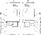
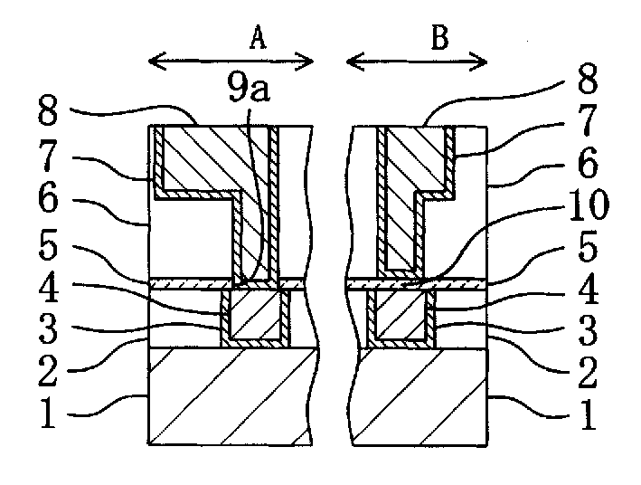
下面,参考图9(a)~图9(f),说明与背景技术有关的半导体器件的制造方法,具体而言,为逆熔丝的制造方法。Next, with reference to FIGS. 9( a ) to 9 ( f ), a method of manufacturing a semiconductor device related to the background art, specifically, a method of manufacturing an antifuse will be described.
图9(a)~图9(f)为显示背景技术所涉及的半导体器件的制造方法中的主要工序的剖面图。9( a ) to 9 ( f ) are cross-sectional views showing main steps in the method of manufacturing a semiconductor device according to the background art.
首先,如图9(a)所示,在半导体衬底100上沉积由铝等金属材料制成的布线层101a。需提一下,这里布线层101a可为在铝层的上、下以钛或者氮化钛等为代表的金属材料的叠层结构。接着,在布线层101a上沉积由非晶硅等制成的具有逆熔丝功能的第一绝缘膜102。First, as shown in FIG. 9( a ), a wiring layer 101 a made of a metal material such as aluminum is deposited on a
接着,如图9(b)所示,通过光刻工序及蚀刻工序将布线层101a和第一绝缘膜102图案化而形成布线101。Next, as shown in FIG. 9( b ), the wiring layer 101 a and the first
接着,如图9(c)所示,在半导体衬底100上形成第二绝缘膜103而将布线层101a被图案化所形成的布线101及已图案化了的第一绝缘膜102覆盖起来。Next, as shown in FIG. 9( c ), a second
接着,如图9(d)所示,蚀刻第二绝缘膜103而形成通到第一绝缘膜膜102上面的第一通孔(via hole)104及第二通孔105。需提一下,具有逆熔丝功能的第一绝缘膜102从第一通孔104及第二通孔105的底部露出来。Next, as shown in FIG. 9( d), the second
接着,如图9(e)所示,形成抗蚀膜106以便仅将形成在逆熔丝形成区域9B的第二通孔105覆盖起来。接着,再以抗蚀图案106为屏蔽通过蚀刻除去存在于第一绝缘膜102中第一通孔104底部的部分,以便形成在电路形成区域9A的第一通孔104和布线101连接起来。之后,再除去抗蚀膜106。Next, as shown in FIG. 9(e), a
接着,如图9(f)所示,利用CVD及CMP技术等用金属材料填充第一通孔104及第二通孔105而形成第一孔塞(via plug)107及第二孔塞108。Next, as shown in FIG. 9( f), the first through
如上所述,逆熔丝109形成在逆熔丝形成区域9B中(例如参考专利文献1)。As described above, the antifuse 109 is formed in the
[专利文献1] 日本国公开专利公报特开平6-97171号公报[Patent Document 1] Japanese Laid-Open Patent Gazette, Japanese Patent Application Laid-Open No. 6-97171
然而,在背景技术所涉及的半导体器件的制造方法中,需要一个在逆熔丝形成区域9B以外的区域中,换句话说,电路形成区域9A中,至少形成具有逆熔丝功能的第一绝缘膜102的工序。这样一来,与在逆熔丝形成区域9A中不采用逆熔丝结构的那一情况下的工序相比,亦即在逆熔丝形成区域9A中不形成具有逆熔丝功能的第一绝缘膜102的那一种情况下的工序相比,工序道数增加了,故制造成本增加;因为随着工序数的增加,粒子也增加,所以恐怕产品合格率会下降;与仅将布线101图案化的那种情况相比,将电路形成区域9A中由具有逆熔丝功能的第一绝缘膜102和布线101构成的叠层结构图案化是一件非常困难的事情;而且,如图9(f)所示,恐怕在逆熔丝形成区域9B中具有逆熔丝功能的第一绝缘膜102和电路形成区域9A中的布线101之间会因为第二绝缘膜103埋入不良而出现空隙(void)103a。However, in the method of manufacturing a semiconductor device according to the background art, it is necessary to form at least the first insulating layer having the function of an antifuse in a region other than the
发明内容Contents of the invention
本发明正是为解决上述问题而开发研究出来的,其目的在于:提供一种工序道数减少,而实现了制造成本下降、产品合格率提高等的半导体器件及其制造方法。The present invention is developed and researched to solve the above problems, and its purpose is to provide a semiconductor device and a manufacturing method thereof that reduce the number of process steps, thereby reducing the manufacturing cost and improving the yield of products.
为达到上述目的,本发明所涉及的第一种半导体器件,包括:形成在半导体衬底上由第一金属制成的第一金属图案,形成在第一金属图案上的绝缘膜,以及形成在绝缘膜上由第二金属制成的第二金属图案;绝缘膜具有为防止所述第一金属扩散的阻挡性。In order to achieve the above object, the first semiconductor device involved in the present invention includes: a first metal pattern made of a first metal formed on a semiconductor substrate, an insulating film formed on the first metal pattern, and an insulating film formed on the first metal pattern. A second metal pattern made of a second metal on the insulating film; the insulating film has barrier properties for preventing the diffusion of the first metal.
根据第一半导体器件,能实现可利用金属镶嵌布线形成工序那样的通常的布线形成工序例如铜布线形成工序制造的逆熔丝结构。因此,可实现能用比现有的逆熔丝形成工序的道数还少的工序数来制造的逆熔丝结构。结果是,能够得到生产成本下降、产品合格率提高的半导体器件。According to the first semiconductor device, it is possible to realize an antifuse structure that can be manufactured by a normal wiring forming process such as a damascene wiring forming process, for example, a copper wiring forming process. Therefore, it is possible to realize an anti-fuse structure that can be manufactured with a smaller number of steps than conventional anti-fuse forming steps. As a result, a semiconductor device with reduced production cost and improved yield can be obtained.
在本发明所涉及的第一半导体器件中,最好是绝缘膜中含有扩散来的第一金属。In the first semiconductor device according to the present invention, it is preferable that the insulating film contains the diffused first metal.
这样一来,因为绝缘膜中含有扩散来的第一金属,所以绝缘膜起由于施加电压而能容易地发生绝缘击穿的逆熔丝的作用。In this way, since the first metal diffused is contained in the insulating film, the insulating film functions as an antifuse that can easily cause dielectric breakdown due to voltage application.
在本发明所涉及的第一半导体器件中,最好是第二金属图案形成为下沉到所述绝缘膜内的样子。In the first semiconductor device according to the present invention, preferably, the second metal pattern is formed to sink into the insulating film.
这样一来,因为第二金属图案形成为下沉到所述绝缘膜内的样子,所以绝缘膜起由于施加电压而能容易地发生绝缘击穿的逆熔丝的作用。In this way, since the second metal pattern is formed to sink into the insulating film, the insulating film functions as an antifuse that can easily cause insulation breakdown due to voltage application.
在本发明所涉及的第一半导体器件中,最好是第一金属图案为布线或者孔塞。In the first semiconductor device according to the present invention, preferably, the first metal pattern is a wiring or a plug.
这样一来,能够实现可利用金属镶嵌布线形成工序制造的逆熔丝结构。In this way, it is possible to realize an antifuse structure that can be manufactured by a damascene wiring forming process.
在本发明所涉及的第一半导体器件中,最好是第二金属图案为布线或者孔塞。In the first semiconductor device according to the present invention, preferably, the second metal pattern is a wiring or a plug.
这样一来,能够实现可利用金属镶嵌布线形成工序制造的逆熔丝结构。而且,在第二金属图案为孔塞的情况下,能够减少形成逆熔丝所需的面积。In this way, it is possible to realize an antifuse structure that can be manufactured by a damascene wiring forming process. Also, in the case where the second metal pattern is a via plug, the area required for forming the reverse fuse can be reduced.
本发明所涉及的第二半导体器件,包括:形成在半导体衬底上由第一金属制成的第一金属图案,形成在第一金属图案上的绝缘膜,以及形成在绝缘膜上由第二金属制成的第二金属图案。绝缘膜具有为防止所述第一金属扩散的阻挡性。第二金属图案,形成为:在电路形成区域穿通绝缘膜与第一金属图案导通,同时在逆熔丝形成区域使绝缘膜介于它和第一金属图案之间。The second semiconductor device according to the present invention includes: a first metal pattern made of a first metal formed on a semiconductor substrate, an insulating film formed on the first metal pattern, and a second metal pattern formed on the insulating film. Second metal pattern made of metal. The insulating film has barrier properties for preventing diffusion of the first metal. The second metal pattern is formed to conduct with the first metal pattern through the insulating film in the circuit formation region, and interpose the insulating film between it and the first metal pattern in the reverse fuse formation region.
根据第二半导体器件,能实现可利用金属镶嵌布线形成工序那样的通常的布线形成工序例如铜布线形成工序制造的逆熔丝结构。因此,可实现能用比现有的逆熔丝形成工序的道数还少的工序数来制造的逆熔丝结构。结果是,能够得到生产成本下降、产品合格率提高的半导体器件。According to the second semiconductor device, it is possible to realize an antifuse structure that can be manufactured by a normal wiring forming process such as a damascene wiring forming process, for example, a copper wiring forming process. Therefore, it is possible to realize an anti-fuse structure that can be manufactured with a smaller number of steps than conventional anti-fuse forming steps. As a result, a semiconductor device with reduced production cost and improved yield can be obtained.
在本发明所涉及的第二半导体器件中,最好是绝缘膜中含有扩散来的第一金属。In the second semiconductor device according to the present invention, it is preferable that the insulating film contains the diffused first metal.
这样一来,因为绝缘膜中含有扩散来的第一金属,所以绝缘膜起由于施加电压而能容易地发生绝缘击穿的逆熔丝的作用。In this way, since the first metal diffused is contained in the insulating film, the insulating film functions as an antifuse that can easily cause dielectric breakdown due to voltage application.
在本发明所涉及的第二半导体器件中,最好是第二金属图案形成为下沉到所述绝缘膜内的样子。In the second semiconductor device according to the present invention, preferably, the second metal pattern is formed to sink into the insulating film.
这样一来,因为第二金属图案形成为下沉到绝缘膜内的样子,所以绝缘膜起由于施加电压而能容易地发生绝缘击穿的逆熔丝的作用。In this way, since the second metal pattern is formed to sink into the insulating film, the insulating film functions as an antifuse that can easily cause dielectric breakdown due to voltage application.
在本发明所涉及的第二半导体器件中,最好是第一金属图案为布线或者孔塞。In the second semiconductor device according to the present invention, preferably, the first metal pattern is a wiring or a plug.
这样一来,能够实现可利用金属镶嵌布线形成工序制造的逆熔丝结构。In this way, it is possible to realize an antifuse structure that can be manufactured by a damascene wiring forming process.
在本发明所涉及的第二半导体器件中,最好是第二金属图案为布线或者孔塞。In the second semiconductor device according to the present invention, preferably, the second metal pattern is a wiring or a plug.
这样一来,能够实现可利用金属镶嵌布线形成工序制造的逆熔丝结构。而且,在第二金属图案为孔塞的情况下,能够减少形成逆熔丝所需的面积。In this way, it is possible to realize an antifuse structure that can be manufactured by a damascene wiring forming process. Also, in the case where the second metal pattern is a via plug, the area required for forming the reverse fuse can be reduced.
本发明所涉及的第一半导体器件的制造方法,包括:在半导体衬底上形成由第一金属制成的布线的步骤,在布线上形成第一绝缘膜的步骤,在第一绝缘膜上形成第二绝缘膜的步骤,在电路形成区域及逆熔丝形成区域中第二绝缘膜上分别形成位于布线的上方同时让第一绝缘膜露出的开口部分的步骤,形成抗蚀图案以覆盖逆熔丝形成区域的开口部分之后,再用该抗蚀图案作屏蔽进行蚀刻,把从电路形成区域的开口部分的底部露出的第一绝缘膜除去而让布线露出的步骤,以及除去抗蚀图案以后,在电路形成区域的开口部分及逆熔丝形成区域的开口部分分别埋入第二金属而形成金属图案的步骤;第一绝缘膜具有防止第一金属扩散的阻挡性。The manufacturing method of the first semiconductor device according to the present invention includes the steps of forming a wiring made of a first metal on a semiconductor substrate, forming a first insulating film on the wiring, and forming a first insulating film on the first insulating film. The step of the second insulating film, the step of forming an opening portion above the wiring while exposing the first insulating film on the second insulating film in the circuit formation region and the reverse fuse formation region, forming a resist pattern to cover the reverse fuse After the opening of the wire formation region, etching is performed using the resist pattern as a mask, removing the first insulating film exposed from the bottom of the opening of the circuit formation region to expose the wiring, and after removing the resist pattern, The step of burying the second metal in the opening part of the circuit formation region and the opening part of the reverse fuse formation region respectively to form a metal pattern; the first insulating film has a barrier property to prevent the diffusion of the first metal.
根据第一半导体器件的制造方法,通过将逆熔丝形成区域的开口部分屏蔽起来进行蚀刻,而边在电路形成区域形成与布线导通的金属图案,边能够在逆熔丝形成区域形成第一绝缘膜成为逆熔丝的结构。于是,能实现可利用金属镶嵌布线形成工序那样的通常的布线形成工序例如铜布线形成工序制造的逆熔丝结构。因此,可实现能用比现有的逆熔丝形成工序的道数还少的工序数来制造的逆熔丝结构。结果是,能够提供一种生产成本下降、产品合格率提高了的半导体器件的制造方法。According to the manufacturing method of the first semiconductor device, by masking the opening portion of the reverse fuse formation region and performing etching, the metal pattern conductive to the wiring is formed in the circuit formation region, and the first semiconductor device can be formed in the reverse fuse formation region. The insulating film becomes the structure of the reverse fuse. Accordingly, it is possible to realize an antifuse structure that can be manufactured by a normal wiring forming process such as a damascene wiring forming process, for example, a copper wiring forming process. Therefore, it is possible to realize an anti-fuse structure that can be manufactured with a smaller number of steps than conventional anti-fuse forming steps. As a result, it is possible to provide a method of manufacturing a semiconductor device with reduced production cost and improved yield.
本发明所涉及的第二半导体器件的制造方法,包括:在半导体衬底上形成由第一金属制成的布线的步骤,在布线上形成第一绝缘膜的步骤,在第一绝缘膜上形成第二绝缘膜的步骤,在电路形成区域及逆熔丝形成区域中第二绝缘膜上分别形成位于布线的上方同时让第一绝缘膜露出的第一开口部分的步骤,在形成为在逆熔丝形成区域的第一开口部分的上部形成第二开口部分的由正型光阻形成的光阻图案之际,以借助曝光不够而形成的正型光阻的残余部分为屏蔽进行蚀刻,而除去电路形成区域中从第一开口部分的底部露出的第一绝缘膜来让布线露出来的步骤,以及除去抗蚀图案之后,在电路形成区域的第一开口部分及逆熔丝形成区域的第一开口部分分别埋入第二金属而形成金属图案的步骤;第一绝缘膜具有防止第一金属扩散的阻挡性。The method for manufacturing a second semiconductor device according to the present invention includes the steps of forming a wiring made of a first metal on a semiconductor substrate, forming a first insulating film on the wiring, and forming a first insulating film on the first insulating film. The step of the second insulating film, the step of forming the first opening portion above the wiring while exposing the first insulating film on the second insulating film in the circuit formation region and the reverse fuse formation region, is formed so that the reverse fuse When the photoresist pattern formed by the positive photoresist of the second opening part is formed on the upper part of the first opening part of the filament formation area, the remaining part of the positive photoresist formed by insufficient exposure is used as a mask to etch to remove The first insulating film exposed from the bottom of the first opening in the circuit formation region to expose the wiring, and after removing the resist pattern, the first opening of the circuit formation region and the first opening of the antifuse formation region The step of forming a metal pattern by embedding the second metal in the openings; the first insulating film has barrier properties to prevent the diffusion of the first metal.
根据第二半导体器件的制造方法,在遮盖起逆熔丝形成区域中的第一开口部分之际,以利用为了形成第二开口部分的由正型光阻形成的光阻图案时的曝光不够而形成的正型光阻的残余部分作屏蔽进行蚀刻,而边在电路形成区域形成与布线导通的金属图案,边能够形成在逆熔丝形成区域第一绝缘膜成为逆熔丝的结构。于是,能实现可利用金属镶嵌布线形成工序那样的通常的布线形成工序例如铜布线形成工序制造的逆熔丝结构。因此,可实现能用比现有的逆熔丝形成工序的道数还少的工序数来制造的逆熔丝结构。结果是,能够提供一种生产成本下降、产品合格率提高了的半导体器件的制造方法。According to the manufacturing method of the second semiconductor device, when the first opening portion in the antifuse formation region is covered, the exposure is insufficient due to the use of the photoresist pattern formed of the positive type photoresist for forming the second opening portion. The remaining part of the formed positive photoresist is used as a mask for etching, and while forming a metal pattern connected to the wiring in the circuit formation area, the first insulating film can be formed in the anti-fuse formation area to become an anti-fuse structure. Accordingly, it is possible to realize an antifuse structure that can be manufactured by a normal wiring forming process such as a damascene wiring forming process, for example, a copper wiring forming process. Therefore, it is possible to realize an anti-fuse structure that can be manufactured with a smaller number of steps than conventional anti-fuse forming steps. As a result, it is possible to provide a method of manufacturing a semiconductor device with reduced production cost and improved yield.
本发明所涉及的第三半导体器件的制造方法,包括:在半导体衬底上形成由第一金属制成的布线的步骤,在布线上形成第一绝缘膜的步骤,进行蚀刻而将第一绝缘膜中存在于电路形成区域的部分薄膜化的步骤;在进行蚀刻的步骤之后,在第一绝缘膜上形成第二绝缘膜的步骤,在电路形成区域第二绝缘膜上形成位于布线的上方并让布线露出的开口部分,同时在逆熔丝形成区域第二绝缘膜上形成位于布线的上方并让第一绝缘膜露出的开口部分的步骤,以及在电路形成区域的开口部分及逆熔丝形成区域的开口部分分别埋入第二金属而形成金属图案的步骤;第一绝缘膜具有防止第一金属扩散的阻挡性。The manufacturing method of the third semiconductor device according to the present invention includes the steps of forming a wiring made of a first metal on a semiconductor substrate, forming a first insulating film on the wiring, and etching the first insulating film. A step of thinning the part of the film that exists in the circuit formation region; after the step of performing etching, a step of forming a second insulation film on the first insulation film, forming a layer located above the wiring on the second insulation film in the circuit formation region. A step of exposing the opening portion of the wiring and simultaneously forming an opening portion above the wiring and exposing the first insulating film on the second insulating film in the reverse fuse formation region, and forming the opening portion in the circuit formation region and the reverse fuse The step of forming a metal pattern by embedding the second metal in the openings of the region; the first insulating film has barrier properties to prevent the diffusion of the first metal.
根据第三半导体器件的制造方法,因为将第一绝缘膜中存在于电路形成区域的部分薄膜化,而逆熔丝形成区域中第一绝缘膜的膜厚还是原来的厚度不变,所以不用将逆熔丝形成区域中的开口部分遮盖起来,就边在电路形成区域形成与布线导通的金属图案,边能够在逆熔丝形成区域形成第一绝缘膜成为逆熔丝的结构。于是,能实现可利用金属镶嵌布线形成工序那样的通常的布线形成工序例如铜布线形成工序制造的逆熔丝结构。因此,可实现能用比现有的逆熔丝形成工序的道数还少的工序数来制造的逆熔丝结构。结果是,能够提供一种生产成本下降、产品合格率提高了的半导体器件的制造方法。According to the manufacturing method of the third semiconductor device, since the portion of the first insulating film existing in the circuit formation region is thinned, the film thickness of the first insulating film in the reverse fuse formation region remains unchanged, so it is not necessary to By covering the opening in the reverse fuse formation region, the first insulating film can be formed in the reverse fuse formation region to form a reverse fuse while forming a metal pattern in the circuit formation region that is conductive to the wiring. Accordingly, it is possible to realize an antifuse structure that can be manufactured by a normal wiring forming process such as a damascene wiring forming process, for example, a copper wiring forming process. Therefore, it is possible to realize an anti-fuse structure that can be manufactured with a smaller number of steps than conventional anti-fuse forming steps. As a result, it is possible to provide a method of manufacturing a semiconductor device with reduced production cost and improved yield.
本发明所涉及的第四半导体器件的制造方法,包括:在半导体衬底上形成由第一金属制成的布线的步骤,在布线上形成第一绝缘膜的步骤,在第一绝缘膜上形成第二绝缘膜的步骤,在第二绝缘膜上形成第三绝缘膜的步骤,进行蚀刻而将第三绝缘膜中存在于电路形成区域的部分除去的步骤,在进行蚀刻的步骤之后,在第二绝缘膜及第三绝缘膜上形成第四绝缘膜的步骤,在电路形成区域第四绝缘膜、第二绝缘膜及第一绝缘膜上形成位于布线的上方并让布线露出的开口部分,同时在逆熔丝形成区域第四绝缘膜、第三绝缘膜及第二绝缘膜上形成位于布线的上方并让第一绝缘膜露出的开口部分的步骤,以及在电路形成区域的开口部分及逆熔丝形成区域的开口部分分别埋入第二金属而形成金属图案的步骤;第一绝缘膜具有防止第一金属扩散的阻挡性。A fourth method of manufacturing a semiconductor device according to the present invention includes the steps of forming a wiring made of a first metal on a semiconductor substrate, forming a first insulating film on the wiring, and forming a first insulating film on the first insulating film. The step of the second insulating film, the step of forming the third insulating film on the second insulating film, the step of etching to remove the part of the third insulating film existing in the circuit formation region, after the step of etching, The step of forming a fourth insulating film on the second insulating film and the third insulating film, forming an opening above the wiring and exposing the wiring on the fourth insulating film, the second insulating film, and the first insulating film in the circuit formation region, and at the same time A step of forming an opening above the wiring and exposing the first insulating film in the fourth insulating film, third insulating film, and second insulating film in the reverse fuse formation region, and the opening and reverse fuse in the circuit formation region The step of forming a metal pattern by burying the openings of the wire formation region with the second metal; the first insulating film has barrier properties to prevent the diffusion of the first metal.
根据第四半导体器件的制造方法,因为除去了第三绝缘膜存在于电路形成区域的部分,所以逆熔丝形成区域中第三绝缘膜便起到了蚀刻停止膜的作用。正因为如此,不用将逆熔丝形成区域中的开口部分遮盖起来,就边在电路形成区域形成与布线导通的金属图案,边能够形成在逆熔丝形成区域第一绝缘膜成为逆熔丝的结构。于是,能实现可利用金属镶嵌布线形成工序那样的通常的布线形成工序例如铜布线形成工序制造的逆熔丝结构。因此,可实现能用比现有的逆熔丝形成工序的道数还少的工序数来制造的逆熔丝结构。结果是,能够提供一种生产成本下降、产品合格率提高了的半导体器件的制造方法。According to the manufacturing method of the fourth semiconductor device, since the portion of the third insulating film existing in the circuit forming region is removed, the third insulating film functions as an etching stopper film in the antifuse forming region. Because of this, the first insulating film can be formed in the reverse fuse formation region as a reverse fuse while forming a metal pattern in the circuit formation region that is conductive to the wiring without covering the opening portion in the reverse fuse formation region. Structure. Accordingly, it is possible to realize an antifuse structure that can be manufactured by a normal wiring forming process such as a damascene wiring forming process, for example, a copper wiring forming process. Therefore, it is possible to realize an anti-fuse structure that can be manufactured with a smaller number of steps than conventional anti-fuse forming steps. As a result, it is possible to provide a method of manufacturing a semiconductor device with reduced production cost and improved yield.
在本发明的第一到第四半导体器件的制造方法中,最好是,形成开口部分的步骤为形成布线沟或者通孔的步骤;在形成开口部分的步骤中形成布线沟的情况下,形成金属图案的步骤为形成布线的步骤,而在形成开口部分的步骤中形成通孔的情况下,形成金属图案的步骤为形成孔塞的步骤。In the first to fourth manufacturing methods of the semiconductor device of the present invention, preferably, the step of forming the opening portion is a step of forming a wiring groove or a via hole; in the case of forming a wiring groove in the step of forming the opening portion, forming The step of forming a metal pattern is a step of forming a wiring, and in the case of forming a via hole in the step of forming an opening portion, the step of forming a metal pattern is a step of forming a plug.
这样一来,便能实现可利用金属镶嵌布线形成工序制造的逆熔丝结构。而且,在金属图案为孔塞的情况下,能够减少形成逆熔丝所需的面积。In this way, an antifuse structure that can be manufactured by a damascene wiring forming process can be realized. Also, in the case where the metal pattern is a via plug, the area required for forming the reverse fuse can be reduced.
本发明所涉及的第五半导体器件的制造方法,包括:在半导体衬底上形成由第一金属制成的孔塞的步骤,在孔塞上形成第一绝缘膜的步骤,在第一绝缘膜上形成第二绝缘膜的步骤,在电路形成区域及逆熔丝形成区域中第二绝缘膜上分别形成位于孔塞的上方同时让第一绝缘膜露出的开口部分的步骤,形成抗蚀图案以覆盖形成在逆熔丝形成区域的开口部分之后,再用该抗蚀图案作屏蔽进行蚀刻,而把电路形成区域中从开口部分的底部露出的第一绝缘膜除去而让孔塞露出的步骤,以及除去抗蚀图案以后,在电路形成区域的开口部分及逆熔丝形成区域的开口部分分别埋入第二金属而形成金属图案的步骤;第一绝缘膜具有防止第一金属扩散的阻挡性。The fifth method of manufacturing a semiconductor device according to the present invention includes: forming a plug made of a first metal on a semiconductor substrate, forming a first insulating film on the plug, and forming a first insulating film on the first insulating film. The step of forming a second insulating film on the circuit formation region and the reverse fuse formation region on the second insulating film respectively forms an opening portion located above the hole plug while exposing the first insulating film, forming a resist pattern to After covering the opening portion formed in the antifuse formation region, etching is performed using the resist pattern as a mask to remove the first insulating film exposed from the bottom of the opening portion in the circuit formation region to expose the hole plug, And after removing the resist pattern, the step of burying the second metal in the opening part of the circuit formation region and the opening part of the reverse fuse formation region respectively to form a metal pattern; the first insulating film has barrier properties to prevent the diffusion of the first metal.
根据第五半导体器件的制造方法,通过覆盖逆熔丝形成区域的开口部分并进行蚀刻,边在电路形成区域形成与布线导通的金属图案,边能够在逆熔丝形成区域形成第一绝缘膜成为逆熔丝的结构。于是,能实现可利用金属镶嵌布线形成工序那样的通常的布线形成工序例如铜布线形成工序制造的逆熔丝结构。因此,可实现能用比现有的逆熔丝形成工序的道数还少的工序数来制造的逆熔丝结构。结果是,能够提供一种生产成本下降、产品合格率提高了的半导体器件的制造方法。According to the fifth manufacturing method of the semiconductor device, the first insulating film can be formed in the reverse fuse formation region while forming the metal pattern conductive to the wiring in the circuit formation region by covering the opening portion of the reverse fuse formation region and performing etching become an antifuse structure. Accordingly, it is possible to realize an antifuse structure that can be manufactured by a normal wiring forming process such as a damascene wiring forming process, for example, a copper wiring forming process. Therefore, it is possible to realize an anti-fuse structure that can be manufactured with a smaller number of steps than conventional anti-fuse forming steps. As a result, it is possible to provide a method of manufacturing a semiconductor device with reduced production cost and improved yield.
在本发明所涉及的第五半导体器件的制造方法中,最好是,形成开口部分的步骤为形成布线沟或者通孔的步骤;在形成开口部分的步骤中形成布线沟的情况下,形成金属图案的步骤为形成布线的步骤,而在形成开口部分的步骤中形成通孔的情况下,形成金属图案的步骤为形成孔塞的步骤。In the manufacturing method of the fifth semiconductor device according to the present invention, it is preferable that the step of forming the opening part is a step of forming a wiring groove or a via hole; The step of patterning is a step of forming wiring, and in the case of forming a via hole in the step of forming an opening portion, the step of forming a metal pattern is a step of forming a plug.
这样一来,便能实现可利用金属镶嵌布线形成工序制造的逆熔丝结构。而且,在金属图案为孔塞的情况下,能够减少形成逆熔丝所需的面积。In this way, an antifuse structure that can be manufactured by a damascene wiring forming process can be realized. Also, in the case where the metal pattern is a via plug, the area required for forming the reverse fuse can be reduced.
在本发明所涉及的第一到第五半导体器件的制造方法中,最好是,第一绝缘膜中含有扩散来的第一金属。In the first to fifth semiconductor device manufacturing methods according to the present invention, it is preferable that the first insulating film contains the diffused first metal.
这样一来,因为第一绝缘膜中含有第一金属,所以绝缘膜起由于电压的施加而能容易地出现绝缘击穿的逆熔丝的作用。In this way, since the first metal is contained in the first insulating film, the insulating film functions as an antifuse that can easily cause dielectric breakdown due to voltage application.
在本发明所涉及的第一到第五半导体器件的制造方法中,最好是,形成在第一绝缘膜上的金属图案形成为下沉到绝缘膜内的样子。In the first to fifth semiconductor device manufacturing methods according to the present invention, preferably, the metal pattern formed on the first insulating film is formed to sink into the insulating film.
这样一来,因为金属图案下沉到绝缘膜内,所以绝缘膜起由于电压的施加而能容易地出现绝缘击穿的逆熔丝的作用。In this way, since the metal pattern sinks into the insulating film, the insulating film functions as an antifuse that can easily cause insulation breakdown due to application of voltage.
—发明的效果——Effects of Invention—
根据本发明所涉及的第一半导体器件,能实现可利用金属镶嵌布线形成工序那样的通常的布线形成工序例如铜布线形成工序制造的逆熔丝结构。因此,可实现能用比现有的逆熔丝形成工序的道数还少的工序数来制造的逆熔丝结构。结果是,能够提供一种生产成本降低、产品合格率提高了的半导体器件。According to the first semiconductor device according to the present invention, it is possible to realize an antifuse structure that can be manufactured by a normal wiring forming process such as a damascene wiring forming process, for example, a copper wiring forming process. Therefore, it is possible to realize an anti-fuse structure that can be manufactured with a smaller number of steps than conventional anti-fuse forming steps. As a result, it is possible to provide a semiconductor device with reduced production cost and improved yield.
根据本发明所涉及的第二半导体器件,能实现可利用金属镶嵌布线形成工序那样的通常的布线形成工序例如铜布线形成工序制造的逆熔丝结构。因此,可实现能用比现有的逆熔丝形成工序的道数还少的工序数来制造的逆熔丝结构。结果是,能够提供一种生产成本降低、产品合格率提高了的半导体器件。According to the second semiconductor device according to the present invention, it is possible to realize an antifuse structure that can be manufactured by a normal wiring forming process such as a damascene wiring forming process, for example, a copper wiring forming process. Therefore, it is possible to realize an anti-fuse structure that can be manufactured with a smaller number of steps than conventional anti-fuse forming steps. As a result, it is possible to provide a semiconductor device with reduced production cost and improved yield.
根据本发明所涉及的第一半导体器件的制造方法,通过将逆熔丝形成区域的开口部分屏蔽起来进行蚀刻,而边在电路形成区域形成与布线导通的金属图案,边能够形成在逆熔丝形成区域第一绝缘膜成为逆熔丝的结构。于是,能实现可利用金属镶嵌布线形成工序那样的通常的布线形成工序例如铜布线形成工序制造的逆熔丝结构。因此,可实现能用比现有的逆熔丝形成工序的道数还少的工序数来制造的逆熔丝结构。结果是,能够提供一种生产成本下降、产品合格率提高了的半导体器件的制造方法。According to the manufacturing method of the first semiconductor device according to the present invention, by masking and etching the opening portion of the reverse fuse formation region, while forming a metal pattern conductive to the wiring in the circuit formation region, it is possible to form a metal pattern in the reverse fuse formation region. The first insulating film in the filament formation region has an antifuse structure. Accordingly, it is possible to realize an antifuse structure that can be manufactured by a normal wiring forming process such as a damascene wiring forming process, for example, a copper wiring forming process. Therefore, it is possible to realize an anti-fuse structure that can be manufactured with a smaller number of steps than conventional anti-fuse forming steps. As a result, it is possible to provide a method of manufacturing a semiconductor device with reduced production cost and improved yield.
根据本发明所涉及的第二半导体器件的制造方法,在遮盖起逆熔丝形成区域中的第一开口部分之际,以利用为了形成第二开口部分的由正型光阻形成的光阻图案时的曝光不够而形成的正型光阻的残余部分作屏蔽进行蚀刻,边在电路形成区域形成与布线导通的金属图案,边能够形成在逆熔丝形成区域第一绝缘膜成为逆熔丝的结构。于是,能实现可利用金属镶嵌布线形成工序那样的通常的布线形成工序例如铜布线形成工序制造的逆熔丝结构。因此,可实现能用比现有的逆熔丝形成工序的道数还少的工序数来制造的逆熔丝结构。结果是,能够提供一种生产成本下降、产品合格率提高了的半导体器件的制造方法。According to the method of manufacturing the second semiconductor device according to the present invention, when the first opening in the reverse fuse formation region is covered, a photoresist pattern formed of a positive photoresist for forming the second opening is used. When the exposure is not enough, the remaining part of the positive photoresist formed as a mask is etched, and a metal pattern that is connected to the wiring is formed in the circuit formation area, and the first insulating film can be formed in the reverse fuse formation area to become a reverse fuse. Structure. Accordingly, it is possible to realize an antifuse structure that can be manufactured by a normal wiring forming process such as a damascene wiring forming process, for example, a copper wiring forming process. Therefore, it is possible to realize an anti-fuse structure that can be manufactured with a smaller number of steps than conventional anti-fuse forming steps. As a result, it is possible to provide a method of manufacturing a semiconductor device with reduced production cost and improved yield.
根据本发明所涉及的第三半导体器件的制造方法,因为将第一绝缘膜中存在于电路形成区域的部分薄膜化,而逆熔丝形成区域中第一绝缘膜的膜厚还是原来的厚度不变,所以不用将逆熔丝形成区域中的开口部分遮盖起来,就边在电路形成区域形成与布线导通的金属图案,边能够形成在逆熔丝形成区域第一绝缘膜成为逆熔丝的结构。于是,能实现可利用金属镶嵌布线形成工序那样的通常的布线形成工序例如铜布线形成工序制造的逆熔丝结构。因此,可实现能用比现有的逆熔丝形成工序的道数还少的工序数来制造的逆熔丝结构。结果是,能够提供一种生产成本下降、产品合格率提高了的半导体器件的制造方法。According to the manufacturing method of the third semiconductor device according to the present invention, since the portion of the first insulating film existing in the circuit formation region is thinned, the film thickness of the first insulating film in the reverse fuse formation region remains the original thickness. Therefore, without covering the opening portion in the reverse fuse formation region, it is possible to form a first insulating film in the reverse fuse formation region to become a reverse fuse while forming a metal pattern conductive to the wiring in the circuit formation region. structure. Accordingly, it is possible to realize an antifuse structure that can be manufactured by a normal wiring forming process such as a damascene wiring forming process, for example, a copper wiring forming process. Therefore, it is possible to realize an anti-fuse structure that can be manufactured with a smaller number of steps than conventional anti-fuse forming steps. As a result, it is possible to provide a method of manufacturing a semiconductor device with reduced production cost and improved yield.
根据本发明所涉及的第四半导体器件的制造方法,因为除去了第三绝缘膜存在于电路形成区域的部分,逆熔丝形成区域中第三绝缘膜便起到了蚀刻停止膜的作用。正因为如此,不用将逆熔丝形成区域中的开口部分遮盖起来,就边在电路形成区域形成与布线导通的金属图案,边能够形成在逆熔丝形成区域第一绝缘膜成为逆熔丝的结构。于是,能实现可利用金属镶嵌布线形成工序那样的通常的布线形成工序例如铜布线形成工序制造的逆熔丝结构。因此,可实现能用比现有的逆熔丝形成工序的道数还少的工序数来制造的逆熔丝结构。结果是,能够提供一种生产成本下降、产品合格率提高了的半导体器件的制造方法。According to the fourth semiconductor device manufacturing method of the present invention, since the portion of the third insulating film existing in the circuit forming region is removed, the third insulating film functions as an etching stopper film in the antifuse forming region. Because of this, the first insulating film can be formed in the reverse fuse formation region as a reverse fuse while forming a metal pattern in the circuit formation region that is conductive to the wiring without covering the opening portion in the reverse fuse formation region. Structure. Accordingly, it is possible to realize an antifuse structure that can be manufactured by a normal wiring forming process such as a damascene wiring forming process, for example, a copper wiring forming process. Therefore, it is possible to realize an anti-fuse structure that can be manufactured with a smaller number of steps than conventional anti-fuse forming steps. As a result, it is possible to provide a method of manufacturing a semiconductor device with reduced production cost and improved yield.
根据本发明所涉及的第五半导体器件的制造方法,通过覆盖逆熔丝形成区域的开口部分并进行蚀刻,边在电路形成区域形成与布线导通的金属图案,边能够形成在逆熔丝形成区域第一绝缘膜成为逆熔丝的结构。于是,能实现可利用金属镶嵌布线形成工序那样的通常的布线形成工序例如铜布线形成工序制造的逆熔丝结构。因此,可实现能用比现有的逆熔丝形成工序的道数还少的工序数来制造的逆熔丝结构。结果是,能够提供一种生产成本下降、产品合格率提高了的半导体器件的制造方法。According to the fifth method of manufacturing a semiconductor device according to the present invention, by covering the opening of the reverse fuse formation region and performing etching, it is possible to form a metal pattern connected to the wiring in the circuit formation region, while forming a metal pattern in the reverse fuse formation region. The first insulating film in the region becomes an antifuse structure. Accordingly, it is possible to realize an antifuse structure that can be manufactured by a normal wiring forming process such as a damascene wiring forming process, for example, a copper wiring forming process. Therefore, it is possible to realize an anti-fuse structure that can be manufactured with a smaller number of steps than conventional anti-fuse forming steps. As a result, it is possible to provide a method of manufacturing a semiconductor device with reduced production cost and improved yield.
附图说明Description of drawings
图1为一主要部分剖面图,显示本发明的第一个实施例所涉及的具有逆熔丝结构的半导体器件的结构。1 is a sectional view of main parts showing the structure of a semiconductor device having an antifuse structure according to a first embodiment of the present invention.
图2为一主要部分剖面图,显示本发明的第一个实施例所涉及的具有逆熔丝结构的半导体器件的结构。2 is a sectional view of main parts showing the structure of a semiconductor device having an antifuse structure according to a first embodiment of the present invention.
图3为一主要部分剖面图,显示本发明的第二个实施例所涉及的具有逆熔丝结构的半导体器件的结构。3 is a sectional view of main parts showing the structure of a semiconductor device having an antifuse structure according to a second embodiment of the present invention.
图4(a)~图4(e)为一说明主要工序的剖面图,显示本发明的第三个实施例所涉及的具有逆熔丝结构的半导体器件的制造方法。4( a ) to 4 ( e ) are cross-sectional views illustrating main processes, showing a method of manufacturing a semiconductor device with an antifuse structure according to a third embodiment of the present invention.
图5(a)~图5(e)为一说明主要工序的剖面图,显示本发明的第四个实施例所涉及的具有逆熔丝结构的半导体器件的制造方法。5( a ) to 5 ( e ) are cross-sectional views illustrating main processes, showing a method of manufacturing a semiconductor device with an antifuse structure according to a fourth embodiment of the present invention.
图6(a)~图6(e)为一说明主要工序的剖面图,显示本发明的第五个实施例所涉及的具有逆熔丝结构的半导体器件的制造方法。6( a ) to 6 ( e ) are cross-sectional views illustrating main processes, showing a method of manufacturing a semiconductor device with an antifuse structure according to a fifth embodiment of the present invention.
图7(a)~图7(f)为一说明主要工序的剖面图,显示本发明的第六个实施例所涉及的具有逆熔丝结构的半导体器件的制造方法。7( a ) to 7 ( f ) are cross-sectional views illustrating main processes, showing a method of manufacturing a semiconductor device with an anti-fuse structure according to a sixth embodiment of the present invention.
图8(a)~图8(e)为一说明主要工序的剖面图,显示本发明的第七个实施例所涉及的具有逆熔丝结构的半导体器件的制造方法。8( a ) to 8 ( e ) are cross-sectional views illustrating main processes, showing a method of manufacturing a semiconductor device with an anti-fuse structure according to a seventh embodiment of the present invention.
图9(a)~图9(f)为一说明主要工序的剖面图,显示现有技术所涉及的具有逆熔丝的半导体器件的制造方法。FIGS. 9( a ) to 9 ( f ) are cross-sectional views illustrating main processes, showing a method of manufacturing a semiconductor device with an antifuse in the prior art.
符号说明Symbol Description
A-电路形成区域;B-逆熔丝形成区域;1-半导体衬底;2、21-第一绝缘膜;3、22-第一阻挡膜;4-第一布线;5、24-第二阻挡膜;6、25、35-第二绝缘膜;7、11、26-第三阻挡膜;8-第二布线;9a、28a-连接孔;10、29、29b-逆熔丝;12、23、27b-孔塞;26b-第三阻挡膜;27-布线;30a、40a-通孔;31a、39a-沟槽;32、33、34、37、41-抗蚀图案;36-第三绝缘膜;38-第四绝缘膜。A-circuit formation area; B-reverse fuse formation area; 1-semiconductor substrate; 2, 21-first insulating film; 3, 22-first barrier film; 4-first wiring; 5, 24-second Barrier film; 6, 25, 35-second insulating film; 7, 11, 26-third barrier film; 8-second wiring; 9a, 28a-connection hole; 10, 29, 29b-reverse fuse; 12, 23, 27b-hole plug; 26b-third barrier film; 27-wiring; 30a, 40a-through hole; 31a, 39a-trench; 32, 33, 34, 37, 41-resist pattern; 36-third Insulating film; 38—the fourth insulating film.
具体实施方式Detailed ways
下面,参考附图,说明本发明的每一个实施例。Next, each embodiment of the present invention will be described with reference to the drawings.
(第一个实施例)(first embodiment)
下面,参考图1及图2,说明本发明的第一个实施例所涉及的具有逆熔丝结构的半导体器件。Next, a semiconductor device having an antifuse structure according to a first embodiment of the present invention will be described with reference to FIGS. 1 and 2 .
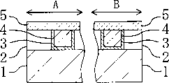
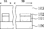
图1为一主要部分剖面图,显示本发明的第一个实施例所涉及的具有逆熔丝结构的半导体器件的结构。需提一下,图1中示出了电路形成区域A及逆熔丝形成区域B。1 is a sectional view of main parts showing the structure of a semiconductor device having an antifuse structure according to a first embodiment of the present invention. Incidentally, FIG. 1 shows a circuit formation region A and an antifuse formation region B. As shown in FIG.
如图1所示,在半导体衬底1上形成第一绝缘膜2。在第一绝缘膜2上形成了含有第一阻挡膜3的由例如铜制成的第一布线(第一金属图案)4。在第一绝缘膜2及第一布线4上形成了第二阻挡膜5。这里,第二阻挡膜5具有防止构成第一布线4的金属扩散的作用,这里是起防止铜扩散的扩散防止膜的作用。第二阻挡膜5上形成了第二绝缘膜6。第二绝缘膜6上形成了含有第三阻挡膜7的例如由铜制成的第二布线(第二金属图案)8。As shown in FIG. 1 , a first
这里,在电路形成区域A,含有第三阻挡膜7的第二布线8,经由贯穿第二阻挡膜5而形成的连接孔9a和第一布线4连接;在逆熔丝形成区域B,因为没给第二阻挡膜5设连接孔,所以含有第三阻挡膜7的第二布线8使第二阻挡膜5介于它和含有第一阻挡膜3的第一布线4之间。Here, in the circuit formation region A, the
这样做以后,在逆熔丝形成区域B中,在作为防止构成第一布线4的铜扩散的扩散防止膜用的第二阻挡膜5中形成了逆熔丝10。于是,逆熔丝10捕捉从第一布线4扩散的金属。因此,可利用逆熔丝10作容易由于施加电压而发生绝缘击穿的逆熔丝用。特别是,在第一布线4由铜制成的该实施例中,因为铜容易扩散到第二阻挡膜5中,所以可使用逆熔丝10作施加电压更容易发生绝缘击穿的逆熔丝用。After doing so, in the reverse fuse formation region B, the
图2示出了上述图1中所示的半导体器件的结构的一个变形。需提一下,和图1中构成部分相同的部分用和图1相同的符号来表示。下面,以不同之处为中心加以说明。FIG. 2 shows a modification of the structure of the semiconductor device shown in FIG. 1 described above. Note that the same components as those in FIG. 1 are denoted by the same symbols as those in FIG. 1 . Hereinafter, the difference will be mainly explained.
在图2所示的半导体器件中,在逆熔丝形成区域B,在第二阻挡膜5上形成了含有第三阻挡膜11的由例如铜制成的孔塞(第二金属图案)12。在图1所示的半导体器件中,在逆熔丝形成区域B形成了第二布线8。这一点是不同的。In the semiconductor device shown in FIG. 2 , in the reverse fuse formation region B, a plug (second metal pattern) 12 made of, for example, copper including a third barrier film 11 is formed on the
这样在第二阻挡膜5上形成孔塞12以后,就能缩小形成逆熔丝10所需的面积。In this way, after the plug 12 is formed on the
另外,因为通过使用氮化硅膜(SiN)或者碳化硅(SiC)膜作图3所示的第二阻挡膜5,防止构成第一布线4的铜扩散的效果就大了,所以能够实现可将所施加的发生绝缘击穿的电压设定得高一些的逆熔丝10。In addition, since by using a silicon nitride film (SiN) or a silicon carbide (SiC) film as the
另外,理想情况为,在逆熔丝形成区域B,第二阻挡膜5比成膜时的表面往下凹,图1所示的第二布线8及图2所示的孔塞12下沉着形成在那一凹下部分。因为若做成这样的结构,第二阻挡膜5就容易在第二阻挡膜5下凹的部分引起绝缘击穿,所以可使用逆熔丝10作容易由于施加电压而发生绝缘击穿的逆熔丝用。In addition, ideally, in the reverse fuse formation region B, the
在该实施例中,说明的是布线或者孔塞所用的材料为铜的那种情况,不仅如此,就是在用铜以外的例如金或者银等贵金属作布线或者孔塞的材料的情况下,本发明也是可实施的。In this embodiment, the description is made of the case where copper is used as the material for wiring or hole plugs. Not only that, but in the case of using noble metals other than copper such as gold or silver as the material for wiring or hole plugs, this Inventions are also enforceable.
(第二个实施例)(second embodiment)
下面,参考图3,说明本发明的第二个实施例所涉及的具有逆熔丝结构的半导体器件。Next, referring to FIG. 3, a semiconductor device having an antifuse structure according to a second embodiment of the present invention will be described.
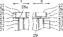
图3为一主要部分剖面图,显示本发明的第二个实施例所涉及的具有逆熔丝结构的半导体器件的结构。3 is a sectional view of main parts showing the structure of a semiconductor device having an antifuse structure according to a second embodiment of the present invention.
如图3所示,在形成在半导体衬底(未示)上的第一绝缘膜21上形成了含有第一阻挡膜22的由例如铜制成的孔塞(第一金属图案)23。在第一绝缘膜21及孔塞23上形成了第二阻挡膜24。这里,第二阻挡膜24起防止构成孔塞23的金属扩散的扩散防止膜的作用,这里是起铜的扩散防止膜的作用。第二阻挡膜24上形成了第二绝缘膜25。第二绝缘膜25上形成了含有第三阻挡膜26的例如由铜制成的布线(第二金属图案)27。As shown in FIG. 3, a plug (first metal pattern) 23 made of, for example, copper containing a
这里,在电路形成区域A,含有第三阻挡膜26的布线27,经由除去第二阻挡膜24而形成的连接孔28a和孔塞23连接;而在逆熔丝形成区域B,因为第二阻挡膜24没设连接孔,所以含有第三阻挡膜26的布线27使第二阻挡膜24介于它和含有第一阻挡膜22的孔塞23之间。Here, in the circuit formation region A, the
这样做以后,在逆熔丝形成区域B中,在作为防止构成孔塞23的铜扩散的膜用的第二阻挡膜24中形成了逆熔丝29。于是,逆熔丝29捕捉从孔塞23扩散的金属。因此,可利用逆熔丝29作容易由于施加电压而发生绝缘击穿的逆熔丝用。特别是,在孔塞23由铜制成的该实施例中,因为铜容易扩散到第二阻挡膜24中,所以可使用逆熔丝29作施加电压更容易发生绝缘击穿的逆熔丝用。After doing so, in the reverse fuse formation region B, the
需提一下,在该实施例中,说明的是在逆熔丝29上形成有布线27的情况,不过和所述第一个实施例一样,可为在逆熔丝29上形成孔塞(未示)的结构。It should be mentioned that, in this embodiment, the case where the
这样在第二阻挡膜24上形成孔塞以后,就能缩小形成逆熔丝所需的面积。In this way, after the plug is formed on the
另外,因为通过使用氮化硅膜(SiN)或者碳化硅(SiC)膜作图1及图2所示的第二阻挡膜24,防止构成孔塞23的铜扩散的效果就大了,所以能够实现可将所施加的发生绝缘击穿的电压设定得高一些的逆熔丝29。In addition, by using a silicon nitride film (SiN) or a silicon carbide (SiC) film as the
另外,理想情况为:在逆熔丝形成区域B,第二阻挡膜24比成膜时的表面往下凹,图3所示的布线27或者代替布线27而形成的孔塞下沉到那一凹下部分。因为若做成这样的结构,第二阻挡膜24就容易在第二阻挡膜24下凹的部分引起绝缘击穿,所以可使用逆熔丝29作容易由于施加电压而发生绝缘击穿的逆熔丝用。In addition, ideally, in the reverse fuse formation region B, the
在该实施例中,说明的是布线或者孔塞所用的材料为铜的那种情况,不仅如此,就是在用铜以外的例如金或者银等贵金属作布线或者孔塞的材料的情况下,本发明也是可实施的。In this embodiment, the description is made of the case where copper is used as the material for wiring or hole plugs. Not only that, but in the case of using noble metals other than copper such as gold or silver as the material for wiring or hole plugs, this Inventions are also enforceable.
(第三个实施例)(third embodiment)
下面,参考图4(a)~图4(e),说明本发明的第三个实施例所涉及的具有逆熔丝结构的半导体器件的制造方法。Next, referring to FIGS. 4( a ) to 4 ( e ), a method of manufacturing a semiconductor device having an antifuse structure according to a third embodiment of the present invention will be described.
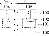
图4(a)~图4(e)为一表示主要工序的剖面图,显示本发明的第三个实施例所涉及的具有逆熔丝结构的半导体器件的制造方法。需提一下,图4中和图1中构成部分共同的部分用和图1相同的符号来表示。4( a ) to 4 ( e ) are cross-sectional views showing main processes, showing a method of manufacturing a semiconductor device with an anti-fuse structure according to a third embodiment of the present invention. It should be noted that the components in FIG. 4 that are common to those in FIG. 1 are denoted by the same symbols as those in FIG. 1 .
首先,如图4(a)所示,在半导体衬底1上形成第一绝缘膜2之后,再在该第一绝缘膜2上形成含有第一阻挡膜3的由例如铜制成的第一布线4。接着,在第一绝缘膜2及第一布线4上形成第二阻挡膜5。第二阻挡膜5起防止构成第一布线4的金属扩散的扩散防止膜的作用,这里是起铜的扩散防止膜的作用。而且,在形成上层的通孔时第二阻挡膜5还起蚀刻停止膜的作用。First, as shown in FIG. 4(a), after forming a first
接着,如图4(b)所示,在第二阻挡膜5上形成第二绝缘膜6以后,再在该第二绝缘膜6上形成通孔30a及沟槽31a。第二绝缘膜6可形成在种类不同的多个层中。而且,象例如在底层的布线上形成绝缘膜的情况等那样,在需要减轻阶梯的处理的情况下,可进行CMP技术等平坦化处理。Next, as shown in FIG. 4( b ), after the second
接着,如图4(c)所示,在电路形成区域A,让与第一布线4即下层布线连接的通孔30a露出来不变,同时在逆熔丝形成区域B,形成抗蚀图案32以便覆盖不让与第一布线4即下层布线连接的通孔30a。Next, as shown in FIG. 4(c), in the circuit formation region A, the through
接着,如图4(d)所示,以抗蚀图案32为屏蔽进行蚀刻,在电路形成区域A的第二阻挡膜5中形成通到第一布线4的连接孔9a。这样一来,在电路形成区域A,通孔30a便和第一布线4即下层布线连接。之后,除去抗蚀图案32。Next, as shown in FIG. 4( d ), etching is performed using the resist
接着,如图4(e)所示,在电路形成区域A,连接孔9a、通孔30a及沟槽31a形成含有第三阻挡膜7的由例如铜制成的第二布线8,在逆熔丝形成区域B,通孔30a及沟槽31a形成含有第三阻挡膜7的由例如铜制成的第二布线8。可利用溅射技术、CVD技术或者电镀技术等埋入金属材料(这里例如为铜)之后,再利用CMP技术除去无用的部分,这样来形成第二布线8。Next, as shown in FIG. 4( e), in the circuit formation region A, the
就这样,因为在逆熔丝形成区域B中没在第二阻挡膜5中形成连接孔,所以含有第三阻挡膜7的第二布线(金属图案)8使第二阻挡膜5介于它和第一阻挡膜3的第一布线4之间。换句话说,在逆熔丝形成区域B,在位于不与第一布线4连接的第二布线8的下层、作为防止构成第一布线4的铜扩散的膜用的第二阻挡膜5中形成逆熔丝10。In this way, since no connection hole is formed in the
如上所述,根据本发明的实施例,可利用以例如铜布线为代表的金属镶嵌(damascene)即通常的布线形成工序形成逆熔丝10。因此,这时所需要的工序道数便比现有的逆熔丝形成工序的道数少。结果是,能够降低成本、提高产品合格率。As described above, according to the embodiment of the present invention, the
需提一下,在该实施例中,没有对通孔30a、沟槽31a的形成顺序做特别的说明,先形成通孔30a或者先形成沟槽31a皆可。It should be mentioned that in this embodiment, there is no special description on the order of forming the through
需提一下,在该实施例中,说明的是形成在逆熔丝10上的第二布线8是通过将金属材料埋入通孔30a及沟槽31a内而形成的这样的结构,不仅如此,即使在不形成沟槽31a,仅形成通孔30a,在逆熔丝10上仅形成孔塞的情况下,也能形成逆熔丝10。在这一情况下,能够缩小形成逆熔丝10所必需的面积。It should be mentioned that in this embodiment, it is explained that the
在该实施例中,因为通过使用氮化硅膜(SiN)或者碳化硅(SiC)膜作第二阻挡膜5,防止构成第一布线4的铜扩散的效果就大了,所以能够实现可将所施加的发生绝缘击穿的电压设定得高一些的逆熔丝10。In this embodiment, since by using a silicon nitride film (SiN) or a silicon carbide (SiC) film as the
另外,理想情况为,在逆熔丝形成区域B,第二阻挡膜5比成膜时的表面往下凹,第二布线8下沉到那一凹下部分。因为若做成这样的结构,第二阻挡膜5就容易在第二阻挡膜5下凹的部分引起绝缘击穿,所以可使用逆熔丝10作容易由于施加电压而发生绝缘击穿的逆熔丝用。In addition, ideally, in the reverse fuse formation region B, the
在该实施例中,说明的是布线或者孔塞所用的材料为铜的那种情况,不仅如此,就是在用铜以外的例如金或者银等贵金属作布线或者孔塞的材料的情况下,本发明也是可实施的。In this embodiment, the description is made of the case where copper is used as the material for wiring or hole plugs. Not only that, but in the case of using noble metals other than copper such as gold or silver as the material for wiring or hole plugs, this Inventions are also enforceable.
(第四个实施例)(fourth embodiment)
下面,参考图5(a)~图5(e),说明本发明的第四个实施例所涉及的具有逆熔丝结构的半导体器件的制造方法。Next, a method of manufacturing a semiconductor device having an antifuse structure according to a fourth embodiment of the present invention will be described with reference to FIGS. 5( a ) to 5 ( e ).
图5(a)~图5(e)为一表示主要工序的剖面图,显示本发明的第四个实施例所涉及的具有逆熔丝结构的半导体器件的制造方法。需提一下,图5(a)~图5(e)中与图1中所示的构成部分相同的部分用相同的符号来表示。5( a ) to 5 ( e ) are cross-sectional views showing main processes, showing a method for manufacturing a semiconductor device with an antifuse structure according to a fourth embodiment of the present invention. Note that, in FIGS. 5( a ) to 5 ( e ), the same components as those shown in FIG. 1 are denoted by the same symbols.
首先,如图5(a)所示,在半导体衬底1上形成第一绝缘膜2之后,再在该第一绝缘膜2上形成含有第一阻挡膜3的由例如铜制成的第一布线4。接着,在第一绝缘膜2及第一布线4上形成第二阻挡膜5。第二阻挡膜5起防止构成第一布线4的金属扩散的扩散防止膜的作用,这里是起铜的扩散防止膜的作用。而且,在形成上层的通孔时第二阻挡膜5还起蚀刻停止膜的作用。First, as shown in FIG. 5(a), after forming a first
接着,如图5(b)所示,在第二阻挡膜5上形成第二绝缘膜6以后,再在该第二绝缘膜6上形成通孔30a。需提一下,第二绝缘膜6可形成在种类不同的多个层中。而且,象例如在底层的布线上形成绝缘膜的情况等那样,在需要减轻阶梯的处理的情况下,可进行CMP技术等平坦化处理。Next, as shown in FIG. 5( b ), after the second
接着,如图5(c)所示,在电路形成区域A,让与第一布线4即下层布线连接的通孔30a露出来不变,同时在逆熔丝形成区域B,用正抗蚀剂形成抗蚀图案33以便覆盖不让与第一布线4即下层布线连接的通孔30a。此时,形成抗蚀图案33时要做到:形成在不与第一布线4连接的通孔30a上的沟槽的图案宽度和通孔30a的宽度一样宽。或者是,布置用以形成沟槽的抗蚀图案而做到由正抗蚀材料将通孔30a的一半以上覆盖起来,这样来使通孔30a内的曝光量不够残余下一部分正抗蚀材料,最后由残余下的那一部分正抗蚀材料形成抗蚀图案33。这里,所形成的沟槽的图案宽度比通孔的图案宽度大0.2μm。Next, as shown in FIG. 5(c), in the circuit formation region A, the through
接着,如图5(d)所示,以抗蚀图案33为屏蔽进行蚀刻而形成沟槽31a。此时,因为在电路形成区域A中,在第二阻挡膜5中形成穿通该第二阻挡膜5且通到第一布线4的连接孔9a,所以通孔30a和第一布线4即下层的布线连接。之后,除去抗蚀图案33。Next, as shown in FIG. 5( d ), etching is performed using the resist
接着,如图5(e)所示,在电路形成区域A,在连接孔9a、通孔30a及沟槽31a形成含有第三阻挡膜7的由例如铜制成的第二布线(金属图案)8,在逆熔丝形成区域B,在通孔30a及沟槽31a形成含有第三阻挡膜7的由例如铜制成的第二布线8。可利用溅射技术、CVD技术或者电镀技术等埋入金属材料(这里例如为铜)之后,再利用CMP技术除去无用的部分,这样来形成第二布线8。Next, as shown in FIG. 5(e), in the circuit formation region A, a second wiring (metal pattern) made of, for example, copper including the
就这样,因为在逆熔丝形成区域B中没在第二阻挡膜5中形成连接孔,所以含有第三阻挡膜7的第二布线8使第二阻挡膜5介于它和含有第一阻挡膜3的第一布线4之间。换句话说,在逆熔丝形成区域B,在位于不与第一布线4连接的第二布线8的下层、作为防止构成第一布线4的铜扩散的膜用的第二阻挡膜5中形成逆熔丝10。In this way, since no connection hole is formed in the
如上所述,根据该实施例所涉及的半导体器件的制造方法,能够利用以例如铜布线为代表的金属镶嵌工序即通常的布线形成工序形成逆熔丝10。因此,这时所需要的工序道数便比现有的逆熔丝形成工序的道数少。结果是,能够降低成本、提高产品合格率。As described above, according to the method of manufacturing a semiconductor device according to this embodiment, the
需提一下,在该实施例中,没有对通孔30a、沟槽31a的形成顺序做特别的说明,先形成通孔30a或者先形成沟槽31a皆可。It should be mentioned that in this embodiment, there is no special description on the order of forming the through
需提一下,在该实施例中,说明的是形成在逆熔丝10上的第二布线8是通过将金属材料埋入通孔30a及沟槽31a内而形成的这样的结构,不仅如此,即使在不形成沟槽31a,仅形成通孔30a,在逆熔丝10上仅形成孔塞的情况下,也能形成逆熔丝10。在这一情况下,能够缩小形成逆熔丝10所必需的面积。It should be mentioned that in this embodiment, it is explained that the
在该实施例中,因为通过使用氮化硅膜(SiN)或者碳化硅(SiC)膜作第二阻挡膜5,防止构成第一布线4的铜扩散的效果就大了,所以能够实现可将所施加的发生绝缘击穿的电压设定得高一些的逆熔丝10。In this embodiment, since by using a silicon nitride film (SiN) or a silicon carbide (SiC) film as the
另外,理想情况为,在逆熔丝形成区域B该区域的第二阻挡膜5比成膜时的表面往下凹,第二布线8下沉到那一凹下部分。因为若做成这样的结构,第二阻挡膜5就容易在第二阻挡膜5下凹的部分引起绝缘击穿,所以可使用逆熔丝10作容易由于施加电压而发生绝缘击穿的逆熔丝用。Ideally, in the reverse fuse formation region B, the
在该实施例中,说明的是布线或者孔塞所用的材料为铜的那种情况,不仅如此,就是在用铜以外的例如金或者银等贵金属作布线或者孔塞的材料的情况下,本发明也是可实施的。In this embodiment, the description is made of the case where copper is used as the material for wiring or hole plugs. Not only that, but in the case of using noble metals other than copper such as gold or silver as the material for wiring or hole plugs, this Inventions are also enforceable.
(第五个实施例)(fifth embodiment)
下面,参考图6(a)~图6(d),说明本发明的第五个实施例所涉及的具有逆熔丝结构的半导体器件的制造方法。Next, a method of manufacturing a semiconductor device having an antifuse structure according to a fifth embodiment of the present invention will be described with reference to FIGS. 6( a ) to 6 ( d ).
图6(a)~图6(d)为一表示主要工序的剖面图,显示本发明的第五个实施例所涉及的具有逆熔丝结构的半导体器件的制造方法。需提一下,图6(a)~图6(d)中与图1中所示的构成部分相同的部分用相同的符号来表示。6( a ) to 6 ( d ) are cross-sectional views showing main processes, showing a method for manufacturing a semiconductor device with an anti-fuse structure according to a fifth embodiment of the present invention. Note that, in FIGS. 6(a) to 6(d), the same components as those shown in FIG. 1 are denoted by the same symbols.
首先,如图6(a)所示,在半导体衬底1上形成第一绝缘膜2之后,再在该第一绝缘膜2上形成含有第一阻挡膜3的由例如铜制成的第一布线4。接着,在第一绝缘膜2及第一布线4上形成第二阻挡膜5。第二阻挡膜5起防止构成第一布线4的金属扩散的扩散防止膜的作用,这里是起铜的扩散防止膜的作用。而且,在形成上层的通孔时第二阻挡膜5还起蚀刻停止膜的作用。First, as shown in FIG. 6(a), after forming a first
接着,如图6(b)所示,在逆熔丝形成区域B的第二阻挡膜5上形成抗蚀图案34。再以抗蚀图案34为屏蔽进行蚀刻,让电路形成区域A中的第二阻挡膜5的膜厚薄一些。之后再除去抗蚀图案34。Next, as shown in FIG. 6( b ), a resist pattern 34 is formed on the
接着,如图6(c)所示,在第二阻挡膜5上形成第二绝缘膜6以后,再在该第二绝缘膜6上形成通孔30a。需提一下,第二绝缘膜6可形成在种类不同的多个层中。而且,象例如在底层的布线上形成绝缘膜的情况等那样,在需要减轻阶梯的处理的情况下,可进行CMP技术等平坦化处理。Next, as shown in FIG. 6( c ), after the second
接着,如图6(d)所示,蚀刻第二绝缘膜6而形成沟槽31a。此时,因为在电路形成区域A中第二阻挡膜5的膜厚薄了,所以通过蚀刻将从通孔30a的底部露出的第二阻挡膜5完全除去,这样来在第二阻挡膜5中形成连接孔9a,通孔30a通到第一布线4。另一方面,在逆熔丝形成区域B,因为第二阻挡膜5的膜厚厚了,所以即使通过蚀刻将从通孔30a的底部露出的第二阻挡膜5除去,通孔30a也通不到第一布线4。Next, as shown in FIG. 6(d), the second
接着,如图6(e)所示,在电路形成区域A,在连接孔9a、通孔30a及沟槽31a形成含有第三阻挡膜7的由例如铜制成的第二布线(金属图案)8,在逆熔丝形成区域B,在通孔30a及沟槽31a形成含有第三阻挡膜7的由例如铜制成的第二布线8。可利用溅射技术、CVD技术或者电镀技术等埋入金属材料(这里例如为铜)之后,再利用CMP技术除去无用的部分,这样来形成第二布线8。Next, as shown in FIG. 6(e), in the circuit formation region A, a second wiring (metal pattern) made of, for example, copper including the
就这样,因为在逆熔丝形成区域B中没在第二阻挡膜5中形成连接孔,所以含有第三阻挡膜7的第二布线8使第二阻挡膜5介于它和含有第一阻挡膜3的第一布线4之间。换句话说,在逆熔丝形成区域B,在位于不与第一布线4连接的第二布线8的下层、作为防止构成第一布线4的铜扩散的膜用的第二阻挡膜5中形成逆熔丝10。In this way, since no connection hole is formed in the
如上所述,根据本发明的实施例,能够利用通常的布线形成工序即以例如铜布线为代表的金属镶嵌工序形成逆熔丝10。因此,这时所需要的工序道数便比现有的逆熔丝形成工序的道数少。结果是,能够降低成本、提高产品合格率。As described above, according to the embodiment of the present invention, the
需提一下,在该实施例中,没有对通孔30a、沟槽31a的形成顺序做特别的说明,先形成通孔30a或者先形成沟槽31a皆可。It should be mentioned that in this embodiment, there is no special description on the order of forming the through
需提一下,在该实施例中,说明的是形成在逆熔丝10上的第二布线8是通过将金属材料埋入通孔30a及沟槽31a内而形成的这样的结构,不仅如此,即使在不形成沟槽31a,仅形成通孔30a,在逆熔丝10上仅形成孔塞的情况下,也能形成逆熔丝10。在这一情况下,能够缩小逆熔丝形成区域B的面积。It should be mentioned that in this embodiment, it is explained that the
在该实施例中,因为通过使用氮化硅膜(SiN)或者碳化硅(SiC)膜作第二阻挡膜5,防止构成第一布线4的铜扩散的效果就大了,所以能够实现可将所施加的发生绝缘击穿的电压设定得高一些的逆熔丝10。In this embodiment, since by using a silicon nitride film (SiN) or a silicon carbide (SiC) film as the
另外,理想情况为,在逆熔丝形成区域B,第二阻挡膜5比成膜时的表面往下凹,第二布线8下沉到那一凹下部分。因为若做成这样的结构,第二阻挡膜5就容易在第二阻挡膜5下凹的部分引起绝缘击穿,所以可使用逆熔丝10作容易由于施加电压而发生绝缘击穿的逆熔丝用。In addition, ideally, in the reverse fuse formation region B, the
在该实施例中,说明的是布线或者孔塞所用的材料为铜的那种情况,不仅如此,就是在用铜以外的例如金或者银等贵金属作布线或者孔塞的材料的情况下,本发明也是可实施的。In this embodiment, the description is made of the case where copper is used as the material for wiring or hole plugs. Not only that, but in the case of using noble metals other than copper such as gold or silver as the material for wiring or hole plugs, this Inventions are also enforceable.
(第六个实施例)(sixth embodiment)
下面,参考图7(a)~图7(f),说明本发明的第六个实施例所涉及的具有逆熔丝结构的半导体器件的制造方法。Next, a method of manufacturing a semiconductor device having an antifuse structure according to a sixth embodiment of the present invention will be described with reference to FIGS. 7( a ) to 7 ( f ).
图7(a)~图7(f)为一表示主要工序的剖面图,显示本发明的第六个实施例所涉及的具有逆熔丝结构的半导体器件的制造方法。需提一下,图7(a)~图7(f)中与图1中所示的构成部分相同的部分用相同的符号来表示。7( a ) to 7 ( f ) are cross-sectional views showing main processes, showing a method of manufacturing a semiconductor device with an anti-fuse structure according to a sixth embodiment of the present invention. Note that, in FIGS. 7( a ) to 7 ( f ), the same components as those shown in FIG. 1 are denoted by the same symbols.
首先,如图7(a)所示,在半导体衬底1上形成第一绝缘膜2之后,再在该第一绝缘膜2上形成含有第一阻挡膜3的由例如铜制成的第一布线4。接着,在第一绝缘膜2及第一布线4上形成第二阻挡膜5。第二阻挡膜5起防止构成第一布线4的金属扩散的扩散防止膜的作用,这里是起铜的扩散防止膜的作用。而且,在形成上层的通孔时第二阻挡膜5还起蚀刻停止膜的作用。接着,再在第二阻挡膜5上依次形成第二绝缘膜35和第三绝缘膜36。First, as shown in FIG. 7(a), after forming a first
接着,如图7(b)所示,在逆熔丝形成区域B的第三绝缘膜36上形成抗蚀图案37。再以抗蚀图案37为屏蔽进行蚀刻而将电路形成区域A中的第三绝缘膜36除去。之后再除去抗蚀图案37。Next, as shown in FIG. 7( b ), a resist
接着,如图7(c)所示,在电路形成区域A中在第二绝缘膜35上形成第四绝缘膜38,在逆熔丝形成区域B第三绝缘膜36上形成第四绝缘膜38。Next, as shown in FIG. 7(c), the fourth insulating
接着,如图7(d)所示,在电路形成区域A中,在第二绝缘膜35及第四绝缘膜38中形成穿通该第二绝缘膜35及第四绝缘膜38而延伸着且通到第二阻挡膜5的通孔30a。另一方面,在逆熔丝形成区域B中第四绝缘膜38上形成穿通该第四绝缘膜38而延伸着且通到第三绝缘膜36的通孔30a。这种情况下,第三绝缘膜36起蚀刻停止膜的作用。Next, as shown in FIG. 7( d ), in the circuit formation region A, a layer extending and passing through the second insulating
接着,如图7(e)所示,蚀刻第四绝缘膜38而形成沟槽31a。此时,在电路形成区域A中,借助蚀刻将从通孔30a的底部露出的第二阻挡膜5除去,而在第二阻挡膜5中形成连接孔9a,通孔30a通到第一布线4。另一方面,在逆熔丝形成区域B,除去第三绝缘膜36及第二绝缘膜35,而让第二阻挡膜5从通孔30a的底部露出。Next, as shown in FIG. 7(e), the fourth insulating
接着,如图7(f)所示,在电路形成区域A中,在连接孔9a、通孔30a及沟槽31a形成含有第三阻挡膜7的由例如铜制成的第二布线(金属图案)8;在逆熔丝形成区域B,在通孔30a及沟槽31a形成含有第三阻挡膜7的由例如铜制成的第二布线8。可利用溅射技术、CVD技术或者电镀技术等埋入金属材料(这里例如为铜)之后,再利用CMP技术除去无用的部分,这样来形成第二布线8。Next, as shown in FIG. 7(f), in the circuit formation region A, a second wiring (metal pattern) made of, for example, copper containing a
就这样,因为在逆熔丝形成区域B中没在第二阻挡膜5中形成连接孔,所以含有第三阻挡膜7的第二布线8使第二阻挡膜5介于它和含有第一阻挡膜3的第一布线4之间。换句话说,在逆熔丝形成区域B,在位于不与第一布线4连接的第二布线8的下层、作为防止构成第一布线4的铜扩散的膜用的第二阻挡膜5中形成逆熔丝10。In this way, since no connection hole is formed in the
如上所述,根据本实施例的半导体器件的制造方法,能够利用以例如铜布线为代表的金属镶嵌工序即通常的布线形成工序形成逆熔丝10。因此,这时所需要的工序道数便比现有的逆熔丝形成工序的道数少。结果是,能够降低成本、提高产品合格率。As described above, according to the semiconductor device manufacturing method of the present embodiment, the
需提一下,在该实施例中,没有对通孔30a、沟槽31a的形成顺序做特别的说明,先形成通孔30a或者先形成沟槽31a皆可。It should be mentioned that in this embodiment, there is no special description on the order of forming the through
需提一下,在该实施例中,说明的是形成在逆熔丝10上的第二布线8是通过将金属材料埋入通孔30a及沟槽31a内而形成的这样的结构,不仅如此,即使在不形成沟槽31a,仅形成通孔30a,在逆熔丝10上仅形成孔塞的情况下,也能形成逆熔丝10。在这一情况下,能够缩小形成逆熔丝10所需要的面积。It should be mentioned that in this embodiment, it is explained that the
在该实施例中,因为通过使用氮化硅膜(SiN)或者碳化硅(SiC)膜作第二阻挡膜5,防止构成第一布线4的铜扩散的效果就大了,所以能够实现可将所施加的发生绝缘击穿的电压设定得高一些的逆熔丝10。In this embodiment, since by using a silicon nitride film (SiN) or a silicon carbide (SiC) film as the
另外,理想情况为,在逆熔丝形成区域B,第二阻挡膜5比成膜时的表面往下凹,第二布线8下沉到那一凹下部分。因为若做成这样的结构,第二阻挡膜5就容易在第二阻挡膜5下凹的部分引起绝缘击穿,所以可使用逆熔丝10作容易由于施加电压而发生绝缘击穿的逆熔丝用。In addition, ideally, in the reverse fuse formation region B, the
在该实施例中,说明的是布线或者孔塞所用的材料为铜的那种情况,不仅如此,就是在用铜以外的例如金或者银等贵金属作布线或者孔塞的材料的情况下,本发明也是可实施的。In this embodiment, the description is made of the case where copper is used as the material for wiring or hole plugs. Not only that, but in the case of using noble metals other than copper such as gold or silver as the material for wiring or hole plugs, this Inventions are also enforceable.
(第七个实施例)(seventh embodiment)
下面,参考图8(a)~图8(e),说明本发明的第七个实施例所涉及的具有逆熔丝结构的半导体器件的制造方法。Next, a method of manufacturing a semiconductor device having an antifuse structure according to a seventh embodiment of the present invention will be described with reference to FIGS. 8( a ) to 8 ( e ).
图8(a)~图8(e)为一表示主要工序的剖面图,显示本发明的第七个实施例所涉及的具有逆熔丝结构的半导体器件的制造方法。需提一下,图8(a)~图8(e)中与图3中所示的构成部分相同的部分用相同的符号来表示。8( a ) to 8 ( e ) are cross-sectional views showing main processes, showing a method of manufacturing a semiconductor device with an anti-fuse structure according to a seventh embodiment of the present invention. Note that, in FIGS. 8( a ) to 8 ( e ), the same components as those shown in FIG. 3 are denoted by the same symbols.
如图8(a)所示,在例如半导体衬底(未示)上形成第一绝缘膜21以后,再在该第一绝缘膜21上形成含有第一阻挡膜22的由例如铜制成的孔塞23。接着,在第一绝缘膜21及孔塞23上形成第二阻挡膜24。这里,第二阻挡膜24起防止构成孔塞23的金属扩散的扩散防止膜的作用,这里是起铜的扩散防止膜的作用。而且,第二阻挡膜24在形成上层的通孔时起蚀刻停止膜的作用。As shown in FIG. 8( a), after forming a first insulating
接着,如图8(b)所示,在第二阻挡膜24上形成第二绝缘膜25以后,再在电路形成区域A中第二绝缘膜25上形成沟槽29a。另一方面,在逆熔丝形成区域B中,在第二绝缘膜25上形成通孔40a。Next, as shown in FIG. 8(b), after the second insulating
接着,如图8(c)所示,形成抗蚀图案41以便将形成在逆熔丝形成区域B中的通孔40a覆盖起来。Next, as shown in FIG. 8(c), a resist pattern 41 is formed so as to cover the via hole 40a formed in the reverse fuse formation region B. Referring to FIG.
接着,如图8(d)所示,以抗蚀图案41为屏蔽进行蚀刻而将从形成在电路形成区域A中的沟槽39a的底部露出来的第二阻挡膜24除去,而形成连接孔28a,让孔塞23露出来。之后,再除去抗蚀图案41。Next, as shown in FIG. 8( d ), the
接着,如图8(e)所示,在电路形成区域A中,在连接孔28a、沟槽39a形成含有第三阻挡膜26的由例如铜制成的布线(金属图案)27,同时在逆熔丝形成区域B通孔40a中形成含有第三阻挡膜26b的由例如铜制成的孔塞(金属图案)27b。可利用溅射技术、CVD技术或者电镀技术等埋入金属材料(这里例如为铜)之后,再利用CMP技术除去无用的部分,这样来形成布线27及27b。Next, as shown in FIG. 8(e), in the circuit formation region A, a wiring (metal pattern) 27 made of, for example, copper including the
就这样,因为在逆熔丝形成区域B中没在第二阻挡膜24中形成连接孔,所以含有第三阻挡膜26b的孔塞27b使第二阻挡膜24介于它和含有第一阻挡膜22的孔塞23之间。换句话说,在逆熔丝形成区域B,在位于不与孔塞23连接的孔塞27b的下层、作为防止构成孔塞23的铜扩散的膜用的第二阻挡膜24中形成逆熔丝29b。In this way, since the connection hole is not formed in the
如上所述,根据该实施例所涉及的半导体器件的制造方法,能够利用以例如铜布线为代表的金属镶嵌工序即通常的布线形成工序形成逆熔丝29b。因此,这时所需要的工序道数便比现有的逆熔丝形成工序的道数少。结果是,能够降低成本、提高产品合格率。As described above, according to the method of manufacturing a semiconductor device according to this embodiment, the antifuse 29b can be formed by a damascene process typified by, for example, copper wiring, that is, a normal wiring forming process. Therefore, the number of process steps required at this time is less than that of the conventional reverse fuse forming process. As a result, the cost can be reduced and the yield of products can be improved.
需提一下,在该实施例中,说明的是在逆熔丝29b上形成孔塞27b的情况,不仅如此,与所述第二个实施例中的图3一样,也可在逆熔丝29b上形成布线这样的结构。但是,与图3所示的结构相比,该实施例中形成逆熔丝所需的面积更小。It should be mentioned that in this embodiment, the description is the case where the
在该实施例中,因为通过使用氮化硅膜(SiN)或者碳化硅(SiC)膜作第二阻挡膜24,防止构成孔塞23的铜扩散的效果就大了,所以能够实现可将所施加的发生绝缘击穿的电压设定得高一些的逆熔丝29b。In this embodiment, since by using a silicon nitride film (SiN) or a silicon carbide (SiC) film as the
另外,理想情况为:在逆熔丝形成区域B,第二阻挡膜24比成膜时的表面往下凹,孔塞27b下沉到那一凹下部分。因为若做成这样的结构,第二阻挡膜24就容易在孔塞27b下凹的部分引起绝缘击穿,所以可使用逆熔丝29b作容易由于施加电压而发生绝缘击穿的逆熔丝用。In addition, ideally, in the reverse fuse formation region B, the
在该实施例中,说明的是布线或者孔塞所用的材料为铜的那种情况,不仅如此,就是在用铜以外的例如金或者银等贵金属作布线或者孔塞的材料的情况下,本发明也是可实施的。In this embodiment, the description is made of the case where copper is used as the material for wiring or hole plugs. Not only that, but in the case of using noble metals other than copper such as gold or silver as the material for wiring or hole plugs, this Inventions are also enforceable.
—实用性—— Practicality —
综上所述,本发明适于半导体器件及其制造方法。特别适于在可再构成的逻辑元件即FPGA(Field Programmable Gate Array)元件中所用的逆熔丝结构及其制造方法。In summary, the present invention is suitable for a semiconductor device and its manufacturing method. It is especially suitable for the antifuse structure used in reconfigurable logic elements, that is, FPGA (Field Programmable Gate Array) elements and its manufacturing method.
Claims (19)
Applications Claiming Priority (2)
| Application Number | Priority Date | Filing Date | Title |
|---|---|---|---|
| JP2003192675 | 2003-07-07 | ||
| JP2003192675 | 2003-07-07 |
Publications (1)
| Publication Number | Publication Date |
|---|---|
| CN1577832A true CN1577832A (en) | 2005-02-09 |
Family
ID=33562419
Family Applications (1)
| Application Number | Title | Priority Date | Filing Date |
|---|---|---|---|
| CNA2004100621554A Pending CN1577832A (en) | 2003-07-07 | 2004-07-05 | Semiconductor device and method for fabricating the same |
Country Status (3)
| Country | Link |
|---|---|
| US (2) | US20050006773A1 (en) |
| CN (1) | CN1577832A (en) |
| TW (1) | TW200504935A (en) |
Cited By (1)
| Publication number | Priority date | Publication date | Assignee | Title |
|---|---|---|---|---|
| CN115148703A (en) * | 2022-06-29 | 2022-10-04 | 上海集成电路装备材料产业创新中心有限公司 | Interconnection structure and preparation method thereof |
Families Citing this family (3)
| Publication number | Priority date | Publication date | Assignee | Title |
|---|---|---|---|---|
| JP5139689B2 (en) * | 2007-02-07 | 2013-02-06 | セイコーインスツル株式会社 | Semiconductor device and manufacturing method thereof |
| JP2016528401A (en) * | 2013-08-15 | 2016-09-15 | サビック グローバル テクノロジーズ ベスローテン フェンノートシャップ | Shear spun submicrometer fiber |
| US10270075B2 (en) | 2015-07-09 | 2019-04-23 | E I Du Pont De Nemours And Company | Separator having adhesive layer, manufacturing method of the same, and electrochemical device having the same |
Family Cites Families (15)
| Publication number | Priority date | Publication date | Assignee | Title |
|---|---|---|---|---|
| US5272101A (en) * | 1990-04-12 | 1993-12-21 | Actel Corporation | Electrically programmable antifuse and fabrication processes |
| US5602053A (en) * | 1996-04-08 | 1997-02-11 | Chartered Semidconductor Manufacturing Pte, Ltd. | Method of making a dual damascene antifuse structure |
| US6025226A (en) * | 1998-01-15 | 2000-02-15 | International Business Machines Corporation | Method of forming a capacitor and a capacitor formed using the method |
| US6021079A (en) * | 1998-05-13 | 2000-02-01 | Richard Mann | Fast, low cost method of developing code for contact programmable ROMs |
| US6515343B1 (en) * | 1998-11-19 | 2003-02-04 | Quicklogic Corporation | Metal-to-metal antifuse with non-conductive diffusion barrier |
| US6251710B1 (en) * | 2000-04-27 | 2001-06-26 | International Business Machines Corporation | Method of making a dual damascene anti-fuse with via before wire |
| US6833604B2 (en) * | 2000-10-03 | 2004-12-21 | Broadcom Corporation | High density metal capacitor using dual-damascene copper interconnect |
| US6809398B2 (en) * | 2000-12-14 | 2004-10-26 | Actel Corporation | Metal-to-metal antifuse structure and fabrication method |
| JP2002305242A (en) * | 2001-04-05 | 2002-10-18 | Canon Sales Co Inc | Method for manufacturing semiconductor device |
| US6541792B1 (en) * | 2001-09-14 | 2003-04-01 | Hewlett-Packard Development Company, Llp | Memory device having dual tunnel junction memory cells |
| US6943065B2 (en) * | 2002-03-25 | 2005-09-13 | Micron Technology Inc. | Scalable high performance antifuse structure and process |
| JP3590034B2 (en) * | 2002-04-26 | 2004-11-17 | Necエレクトロニクス株式会社 | Semiconductor capacitive element and manufacturing method thereof |
| US6709918B1 (en) * | 2002-12-02 | 2004-03-23 | Chartered Semiconductor Manufacturing Ltd. | Method for making a metal-insulator-metal (MIM) capacitor and metal resistor for a copper back-end-of-line (BEOL) technology |
| JP3811473B2 (en) * | 2003-02-25 | 2006-08-23 | 富士通株式会社 | Semiconductor device |
| US20050035429A1 (en) * | 2003-08-15 | 2005-02-17 | Yeh Chih Chieh | Programmable eraseless memory |
-
2004
- 2004-07-05 CN CNA2004100621554A patent/CN1577832A/en active Pending
- 2004-07-07 TW TW093120396A patent/TW200504935A/en unknown
- 2004-07-07 US US10/884,998 patent/US20050006773A1/en not_active Abandoned
-
2006
- 2006-11-17 US US11/600,844 patent/US20070057376A1/en not_active Abandoned
Cited By (1)
| Publication number | Priority date | Publication date | Assignee | Title |
|---|---|---|---|---|
| CN115148703A (en) * | 2022-06-29 | 2022-10-04 | 上海集成电路装备材料产业创新中心有限公司 | Interconnection structure and preparation method thereof |
Also Published As
| Publication number | Publication date |
|---|---|
| TW200504935A (en) | 2005-02-01 |
| US20050006773A1 (en) | 2005-01-13 |
| US20070057376A1 (en) | 2007-03-15 |
Similar Documents
| Publication | Publication Date | Title |
|---|---|---|
| CN1290186C (en) | Semiconductor device and method for manufacturing the same | |
| CN1231970C (en) | Semiconductor device | |
| CN1311547C (en) | Semiconductor device and manufacturing method thereof, circuit substrate and electronic device | |
| CN1701418A (en) | Semiconductor device producing method, semiconductor wafer and semiconductor device | |
| CN1309077C (en) | Semiconductor device comprising low dielectric material film and its production method | |
| CN1174409A (en) | Semiconductor device and manufacturing method thereof | |
| CN1956173A (en) | Semiconductor device and method of manufacture thereof | |
| CN1677658A (en) | Semiconductor device and method for manufacturing the same | |
| CN1819157A (en) | Semiconductor device | |
| CN1499626A (en) | Semiconductor device and manufacturing method thereof | |
| CN1967800A (en) | Process for producing semiconductor integrated circuit device | |
| CN1617312A (en) | Semiconductor device and method for fabricating the same | |
| CN1416170A (en) | Semiconductor device and mfg. method thereof | |
| CN1738002A (en) | Manufacturing method of semiconductor device | |
| CN1445848A (en) | Semiconductor device, manufacturing method thereof, and phase shift mask | |
| CN1870259A (en) | Multilayer wiring substrate | |
| CN1476072A (en) | Semiconductor device with a plurality of transistors | |
| CN101066005A (en) | Multilayer wiring board and method for manufacturing same | |
| CN101044605A (en) | Semiconductor device and its making method | |
| CN1426106A (en) | Semiconductor device | |
| CN101030557A (en) | Semiconductor device and process for producing the same | |
| CN101034693A (en) | Semiconductor device and method for manufacturing semiconductor device | |
| CN1855467A (en) | Semiconductor device and method of manufacturing same | |
| CN1601741A (en) | Semiconductor device and manufacturing method thereof | |
| CN1444279A (en) | Semiconductor device and its mfg. method |
Legal Events
| Date | Code | Title | Description |
|---|---|---|---|
| C06 | Publication | ||
| PB01 | Publication | ||
| C10 | Entry into substantive examination | ||
| SE01 | Entry into force of request for substantive examination | ||
| AD01 | Patent right deemed abandoned | ||
| C20 | Patent right or utility model deemed to be abandoned or is abandoned |