CN1578555A - Light emitting display - Google Patents
Light emitting display Download PDFInfo
- Publication number
- CN1578555A CN1578555A CNA2004100476029A CN200410047602A CN1578555A CN 1578555 A CN1578555 A CN 1578555A CN A2004100476029 A CNA2004100476029 A CN A2004100476029A CN 200410047602 A CN200410047602 A CN 200410047602A CN 1578555 A CN1578555 A CN 1578555A
- Authority
- CN
- China
- Prior art keywords
- light
- wavelength
- mentioned
- emitting
- maximum
- Prior art date
- Legal status (The legal status is an assumption and is not a legal conclusion. Google has not performed a legal analysis and makes no representation as to the accuracy of the status listed.)
- Granted
Links
Images


Classifications
-
- H—ELECTRICITY
- H05—ELECTRIC TECHNIQUES NOT OTHERWISE PROVIDED FOR
- H05B—ELECTRIC HEATING; ELECTRIC LIGHT SOURCES NOT OTHERWISE PROVIDED FOR; CIRCUIT ARRANGEMENTS FOR ELECTRIC LIGHT SOURCES, IN GENERAL
- H05B33/00—Electroluminescent light sources
- H05B33/12—Light sources with substantially two-dimensional [2D] radiating surfaces
- H05B33/14—Light sources with substantially two-dimensional [2D] radiating surfaces characterised by the chemical or physical composition or the arrangement of the electroluminescent material, or by the simultaneous addition of the electroluminescent material in or onto the light source
-
- H—ELECTRICITY
- H10—SEMICONDUCTOR DEVICES; ELECTRIC SOLID-STATE DEVICES NOT OTHERWISE PROVIDED FOR
- H10K—ORGANIC ELECTRIC SOLID-STATE DEVICES
- H10K59/00—Integrated devices, or assemblies of multiple devices, comprising at least one organic light-emitting element covered by group H10K50/00
- H10K59/10—OLED displays
- H10K59/12—Active-matrix OLED [AMOLED] displays
- H10K59/123—Connection of the pixel electrodes to the thin film transistors [TFT]
-
- H—ELECTRICITY
- H05—ELECTRIC TECHNIQUES NOT OTHERWISE PROVIDED FOR
- H05B—ELECTRIC HEATING; ELECTRIC LIGHT SOURCES NOT OTHERWISE PROVIDED FOR; CIRCUIT ARRANGEMENTS FOR ELECTRIC LIGHT SOURCES, IN GENERAL
- H05B33/00—Electroluminescent light sources
- H05B33/12—Light sources with substantially two-dimensional [2D] radiating surfaces
- H05B33/22—Light sources with substantially two-dimensional [2D] radiating surfaces characterised by the chemical or physical composition or the arrangement of auxiliary dielectric or reflective layers
-
- H—ELECTRICITY
- H10—SEMICONDUCTOR DEVICES; ELECTRIC SOLID-STATE DEVICES NOT OTHERWISE PROVIDED FOR
- H10K—ORGANIC ELECTRIC SOLID-STATE DEVICES
- H10K50/00—Organic light-emitting devices
- H10K50/80—Constructional details
- H10K50/85—Arrangements for extracting light from the devices
-
- H—ELECTRICITY
- H10—SEMICONDUCTOR DEVICES; ELECTRIC SOLID-STATE DEVICES NOT OTHERWISE PROVIDED FOR
- H10K—ORGANIC ELECTRIC SOLID-STATE DEVICES
- H10K59/00—Integrated devices, or assemblies of multiple devices, comprising at least one organic light-emitting element covered by group H10K50/00
- H10K59/10—OLED displays
- H10K59/12—Active-matrix OLED [AMOLED] displays
-
- H—ELECTRICITY
- H10—SEMICONDUCTOR DEVICES; ELECTRIC SOLID-STATE DEVICES NOT OTHERWISE PROVIDED FOR
- H10K—ORGANIC ELECTRIC SOLID-STATE DEVICES
- H10K59/00—Integrated devices, or assemblies of multiple devices, comprising at least one organic light-emitting element covered by group H10K50/00
- H10K59/80—Constructional details
- H10K59/875—Arrangements for extracting light from the devices
-
- H—ELECTRICITY
- H10—SEMICONDUCTOR DEVICES; ELECTRIC SOLID-STATE DEVICES NOT OTHERWISE PROVIDED FOR
- H10K—ORGANIC ELECTRIC SOLID-STATE DEVICES
- H10K2102/00—Constructional details relating to the organic devices covered by this subclass
- H10K2102/301—Details of OLEDs
- H10K2102/302—Details of OLEDs of OLED structures
- H10K2102/3023—Direction of light emission
- H10K2102/3026—Top emission
-
- H—ELECTRICITY
- H10—SEMICONDUCTOR DEVICES; ELECTRIC SOLID-STATE DEVICES NOT OTHERWISE PROVIDED FOR
- H10K—ORGANIC ELECTRIC SOLID-STATE DEVICES
- H10K2102/00—Constructional details relating to the organic devices covered by this subclass
- H10K2102/301—Details of OLEDs
- H10K2102/351—Thickness
-
- H—ELECTRICITY
- H10—SEMICONDUCTOR DEVICES; ELECTRIC SOLID-STATE DEVICES NOT OTHERWISE PROVIDED FOR
- H10K—ORGANIC ELECTRIC SOLID-STATE DEVICES
- H10K59/00—Integrated devices, or assemblies of multiple devices, comprising at least one organic light-emitting element covered by group H10K50/00
- H10K59/30—Devices specially adapted for multicolour light emission
- H10K59/35—Devices specially adapted for multicolour light emission comprising red-green-blue [RGB] subpixels
Landscapes
- Engineering & Computer Science (AREA)
- Microelectronics & Electronic Packaging (AREA)
- Physics & Mathematics (AREA)
- Optics & Photonics (AREA)
- Electroluminescent Light Sources (AREA)
- Devices For Indicating Variable Information By Combining Individual Elements (AREA)
Abstract
提供一种发光型显示装置,可在宽视角范围内颜色变化很小。该发光型显示装置的特征在于,至少在发光区域中除去在发光元件的发光动作中不需要的膜,在对于从构成上述发光元件的发光层发射的光的干涉的强度在视角为0°时为极大值的波长为λimax,从上述发光层发射的光的强度为最大的波长为λemax时,满足λimax<λemax的关系。
Provided is a light-emitting display device capable of little color change over a wide viewing angle range. This light-emitting display device is characterized in that at least in the light-emitting region, a film unnecessary for the light-emitting operation of the light-emitting element is removed, and when the intensity of interference with light emitted from the light-emitting layer constituting the light-emitting element is 0° when the viewing angle is When λimax is the wavelength at which the maximum value is obtained, and λemax is the wavelength at which the intensity of light emitted from the light-emitting layer becomes maximum, the relationship of λimax<λemax is satisfied.
Description
技术领域technical field
本发明涉及控制以矩阵状配置的发光元件的发光动作而进行显示的发光型显示装置,特别涉及包括具有把相当于或小于等于光的波长的厚度的薄膜相层叠的结构的有机发光二极管元件等发光元件的发光型显示装置。The present invention relates to a light-emitting display device that controls the light-emitting operation of light-emitting elements arranged in a matrix to display, and particularly relates to an organic light-emitting diode element having a structure in which thin films having a thickness equal to or less than the wavelength of light are stacked. A light-emitting display device of a light-emitting element.
背景技术Background technique
有机发光二极管元件,是通过在由有机薄膜组成的发光层中注入正负电荷将电能变换为光能而发光的元件。具有作为发光元件的有机发光二极管元件的发光型显示装置(以下称其为“OLED显示器”),与以液晶显示装置为代表的非发光型的显示装置不同,由于是自发光型,不需要背照光等辅助光源,是一种薄型轻质的装置。此外,OLED显示器具有视角广、显示的响应速度快的特征。An organic light-emitting diode device is a device that emits light by injecting positive and negative charges into a light-emitting layer composed of an organic thin film to convert electrical energy into light energy. A light-emitting display device having an organic light-emitting diode element as a light-emitting element (hereinafter referred to as an "OLED display") is different from a non-light-emitting display device represented by a liquid crystal display device. Auxiliary light sources such as lighting are thin and lightweight devices. In addition, the OLED display has the characteristics of wide viewing angle and fast display response speed.
作为有机发光二极管元件70,公知的有由图16例示的元件,其由在透明基板6上形成的用作阳极的透明电极200、由反光性金属构成的用作阴极的反射电极300、以及在这些电极之间的从阴极侧起顺序层叠电子输送层101、发光层102、空穴输送层103的三层结构的有机膜100组成。构成有机发光二极管元件70的这些薄膜的厚度一般为数十至数百nm,相当于或小于等于光的波长,因为反射电极是镜面,从发光层发射的光受到干涉的影响。在有机发光二极管元件70中存在以下的问题:由于干涉作用,实际上射向观察者1000的光2000的发光光谱是随着视角而改变的,并且颜色也改变。在无机电致发光元件中也存在与此同样的问题。As the organic light
针对这一问题,在下面的专利文献1、2中公开了在发光元件中设置使光散射的结构。In response to this problem, the following
[专利文献1]:日本专利特开平11-329742号公报。[Patent Document 1]: Japanese Patent Laid-Open No. H11-329742.
[专利文献2]:日本专利特开2002-270365号公报。[Patent Document 2]: Japanese Patent Application Laid-Open No. 2002-270365.
在这些文献中记载了,从元件发出的光受到光散射体的散射,由于各种行进方向及相位差的互相混合,可大幅度降低由于干涉原因产生的颜色随视角的变化。These documents describe that the light emitted from the device is scattered by the light scatterer, and the color change with the viewing angle due to interference can be greatly reduced due to the mutual mixing of various traveling directions and phase differences.
[专利文献3]:日本专利特开平4-328295号公报。[Patent Document 3]: Japanese Patent Application Laid-Open No. 4-328295.
另外,在专利文献3中,公开了一种通过将电子输送层的膜厚做成包含膜厚辉度衰减特性的二次极大值并且产生其振幅超过其会聚辉度值的辉度的膜厚,可降低由于干涉原因产生的颜色随视角的变化。它是一种在发光层发射的光中,着眼于由于射向直接观察者侧的光和由背面电极反射之后射向观察者侧的光的相位差产生的干涉,根据电子输送层的膜厚辉度衰减特性设定条件的元件。In addition, Patent Document 3 discloses a film that generates a luminance whose amplitude exceeds its converged luminance value by making the film thickness of the electron transport layer include a second-order maximum value of the luminance attenuation characteristic of the film thickness. Thick to reduce color variation with viewing angle due to interference. It is a kind of light emitted from the light-emitting layer, focusing on the interference caused by the phase difference between the light incident on the direct observer side and the light incident on the observer side after being reflected by the back electrode, according to the film thickness of the electron transport layer Component for setting conditions of luminance attenuation characteristics.
[专利文献4]:日本专利特开平7-240277号公报。[Patent Document 4]: Japanese Patent Application Laid-Open No. 7-240277.
另外,在专利文献4中,公开了一种作为利用干涉作用的元件,将透明电极和基板的界面、或透明电极和高折射率底层膜的界面、或透明电极和低折射率底层膜的界面作为反射性界面,通过控制从阴极到阳极的光学膜厚而提高发出的光的色纯度的有机发光二极管元件。In addition, Patent Document 4 discloses that as an element utilizing interference, the interface between a transparent electrode and a substrate, or an interface between a transparent electrode and a high-refractive-index underlying film, or an interface between a transparent electrode and a low-refractive-index underlying film is disclosed. An organic light-emitting diode device that improves the color purity of emitted light by controlling the optical film thickness from the cathode to the anode as a reflective interface.
一般认为,OLED显示器的驱动类型分为具有薄膜晶体管(以下也称其为“TFT”)等的开关元件的有源矩阵驱动型和将构成有机发光二极管元件的电极分别直接与扫描线和数据线连接进行驱动的简单矩阵驱动型。It is generally believed that the drive types of OLED displays are divided into active matrix drive types with switching elements such as thin film transistors (hereinafter also referred to as "TFT") and those that directly connect the electrodes constituting organic light emitting diode elements to scan lines and data lines. A simple matrix driver type that is connected and driven.
有源矩阵驱动型OLED显示器的典型像素驱动电路是由开关晶体管和驱动晶体管这两个TFT和存储电容构成,利用此像素驱动电路可以控制有机发光二极管元件的发光。像素配置于把供给数据信号(或者也称为“图像信号”)的n根数据线和供给扫描信号的m根扫描线(以下也称其为“栅线”)排列成为m行×n列的矩阵的各交叉部分上。A typical pixel driving circuit of an active matrix driven OLED display is composed of two TFTs, a switching transistor and a driving transistor, and a storage capacitor. The pixel driving circuit can be used to control the light emission of organic light emitting diode elements. Pixels are arranged in m rows×n columns by arranging n data lines for supplying data signals (or also referred to as “image signals”) and m scanning lines for supplying scanning signals (hereinafter also referred to as “gate lines”). on each intersection of the matrix.
像素的驱动,从最初的(第一行)栅线开始顺序供给接通电压,在一帧期间内对m行栅线顺序供给扫描信号。在这种驱动方法中,在向某一栅线供给接通电压期间,与该数据线连接的开关晶体管全部处于导通状态,与其同步向n列数据线供给数据电压。这是有源矩阵驱动型的液晶显示装置中一般使用的驱动方法。To drive the pixels, an ON voltage is sequentially supplied from the first (first row) gate lines, and scan signals are sequentially supplied to m rows of gate lines within one frame period. In this driving method, while an on-voltage is being supplied to a certain gate line, all switching transistors connected to the data line are in an on-state, and a data voltage is supplied to n-column data lines in synchronization therewith. This is a driving method generally used in an active matrix driving type liquid crystal display device.
在向栅线供给接通电压期间,数据电压存储于存储电容中,大致保持一帧期间。存储电容的电压值,决定驱动晶体管的栅压,由此控制流过驱动晶体管的电流值而控制有机发光二极管元件的发光。就是说,在有源矩阵驱动型的OLED显示器中,可以在一帧期间进行规定的发光。During the period when the on-voltage is supplied to the gate line, the data voltage is stored in the storage capacitor, which is maintained for approximately one frame period. The voltage value of the storage capacitor determines the gate voltage of the drive transistor, thereby controlling the current value flowing through the drive transistor to control the light emission of the organic light emitting diode element. That is, in an active matrix driven OLED display, predetermined light emission can be performed in one frame period.
与此不同,在简单矩阵驱动型OLED显示器中,只在选择某一扫描线期间有机发光二极管元件有电流流过而发光。因此,为了在简单矩阵驱动型OLED显示器中得到像在有源矩阵驱动型OLED显示器中在一帧期间发光时同样的辉度,必需有大致为扫描线数倍的发光辉度。为了实现这一点,驱动有机发光二极管元件的电压和电流必需很大,由于发热等导致的能量损耗会使电力效率降低。In contrast, in a simple matrix-driven OLED display, an organic light emitting diode element emits light only when a certain scanning line is selected. Therefore, in order to obtain the same luminance in a simple matrix drive type OLED display as when light is emitted for one frame period in an active matrix drive type OLED display, it is necessary to have an emission luminance approximately several times that of a scanning line. In order to realize this, the voltage and current for driving the organic light emitting diode element must be large, and energy loss due to heat generation or the like degrades power efficiency.
这样,有源矩阵驱动型与简单矩阵驱动型相比,从降低耗电观点评价更为优越。Thus, the active matrix drive type is superior to the simple matrix drive type in terms of power consumption reduction.
发明内容Contents of the invention
在实现有源矩阵驱动型OLED显示器时,TFT等开关元件是必需的。由于开关元件是对有机发光二极管元件进行电流驱动所必需的,考虑到迁移率高和阈值电压漂移引起的性能劣化,优选使用多晶硅TFT。When realizing an active matrix driven OLED display, switching elements such as TFTs are necessary. Since switching elements are necessary for current driving of organic light emitting diode elements, polysilicon TFTs are preferably used in consideration of high mobility and performance degradation due to threshold voltage drift.
图17为具有低温多晶硅TFT作为开关元件10的现有的OLED显示器的一个像素附近的示意剖面图。当不是在像石英玻璃基板那样的昂贵的基板上,而是在由廉价玻璃基板构成的透明基板6上形成低温多晶硅TFT时,为了防止由于混入Na及K等离子而引起的TFT的阈值电压的变动的问题,在透明基板6上淀积由SiN构成的用来阻挡离子的第1底层膜11和由SiO构成的第2底层膜12。此外,还在透明基板6上层叠构成TFT的栅绝缘膜16及其他层间绝缘膜18、20。FIG. 17 is a schematic cross-sectional view around a pixel of a conventional OLED display having a low-temperature polysilicon TFT as the
这样,在有源矩阵驱动型OLED显示器中,在由包含发光层的有机膜100、透明电极200、反射电极300构成的有机发光二极管元件70和透明基板6之间存在多个折射率不同的膜。由于这些膜的厚度一般为数十nm~数百nm,会对从发光层射出的朝向观察者1000的光2000施加干涉的影响。In this way, in an active matrix driven OLED display, there are a plurality of films with different refractive indices between the organic light
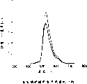
图18为示出现有的有源矩阵驱动型OLED显示器的发光光谱的测定结果的一个示例,是示出绿色发光光谱与视角的依赖关系的示图。当视角改变时,由于光的干涉的影响,发光强度对波长的比率改变。另外,图19为示出现有的有源矩阵驱动型OLED显示器的色度与视角的依赖关系的测定例的示图。此图是在显示红色、绿色和蓝色三原色和白色时的视角在0°~75°之间的色度以15°的间隔绘出的曲线图。这样就产生在现有的有源矩阵驱动型OLED显示器中由于视角而难以容许的颜色的变化。FIG. 18 is an example showing measurement results of the light emission spectrum of a conventional active matrix driven OLED display, and is a graph showing the dependence of the green light emission spectrum on the viewing angle. When the viewing angle changes, the ratio of luminous intensity to wavelength changes due to the influence of interference of light. In addition, FIG. 19 is a graph showing a measurement example of the dependence of chromaticity on a viewing angle in a conventional active matrix driven OLED display. This figure is a graph of the chromaticity plotted at intervals of 15° at viewing angles between 0° and 75° when displaying the three primary colors of red, green, and blue and white. This produces color variations that are difficult to tolerate due to viewing angles in existing active-matrix driven OLED displays.
与此相对,作为抑制颜色随视角变化的方法,现在已经提出的方案有对发光元件设置使光散射的单元。此时,如果设置可以充分抑制干涉的影响的光散射层等散射单元,则在明亮的环境下,从外部进入显示装置的入射光受到散射单元的漫反射,黑显示不够黑而显得发白。因此,就存在在明亮的环境下得不到充分的对比度的问题。On the other hand, as a method of suppressing the change in color depending on the viewing angle, there has been proposed a means to provide light-scattering means to the light-emitting element. At this time, if a scattering unit such as a light scattering layer that can sufficiently suppress the influence of interference is provided, in a bright environment, incident light entering the display device from the outside is diffusely reflected by the scattering unit, and the black display is not black enough to appear whitish. Therefore, there is a problem that sufficient contrast cannot be obtained in a bright environment.
图20为示出现有的有源矩阵驱动型OLED显示器的绿色像素的干涉强度与视角的依赖关系的试算结果的示图。这样,在现有的有源矩阵驱动型OLED显示器中,由于在可见光波长区域也存在在底层膜及层间绝缘膜的界面上的反射引起的干涉强度的极大值和极小值,出现极大值波长和出现极小值的波长的间隔很狭窄,只有数十nm。另外,干涉强度的极大值及极小值随着视角的增大而向着短波长侧移动大约70~140nm。FIG. 20 is a graph showing experimental calculation results of the dependence of the interference intensity of a green pixel on a conventional active-matrix driven OLED display on a viewing angle. In this way, in the existing active matrix driven OLED display, due to the maximum value and the minimum value of the interference intensity caused by the reflection on the interface of the underlying film and the interlayer insulating film also in the visible wavelength region, extremes occur. The interval between the maximum value wavelength and the minimum value wavelength is as narrow as tens of nm. In addition, the maximum value and the minimum value of the interference intensity shift toward the short wavelength side by about 70-140 nm as the viewing angle increases.
因此,通过控制在现有技术中关注的电子输送层的膜厚或从阴极(反射电极)到阳极(透明电极)的光学膜厚,即使是采用由于光的干涉而增强所希望的波长的强度的条件,如图20所示,由于在视角0°时,在比所希望的波长更长的长波长侧存在的干涉强度的极大值及极小值,随着视角从0°变大为30°、45°、60°,会移动到发光波长区域而出现,观察者所观察到的发光光谱也会改变,颜色也会发生变化。Therefore, by controlling the film thickness of the electron transport layer or the optical film thickness from the cathode (reflective electrode) to the anode (transparent electrode) that has been focused on in the prior art, even if the intensity of the desired wavelength is enhanced due to light interference conditions, as shown in Figure 20, since the maximum value and minimum value of the interference intensity existing on the long wavelength side longer than the desired wavelength at the viewing angle of 0°, as the viewing angle increases from 0° to 30°, 45°, 60°, will move to the luminous wavelength region and appear, the luminous spectrum observed by the observer will also change, and the color will also change.
本发明的目的在于提供一种在具有有机发光二极管元件等受到光的干涉影响的发光元件的发光型显示装置中,可实现颜色随视角的变化很小的显示的发光型显示装置。An object of the present invention is to provide a light-emitting display device having a light-emitting element such as an organic light-emitting diode element that is affected by interference of light, which can realize a display with little color change depending on the viewing angle.
现在已经清楚,有源矩阵驱动型OLED显示器的颜色随视角的变化,只借助在现有技术中考虑的电子输送层的膜厚或从阴极到阳极的光学膜厚是不能控制的,而必须考虑在底层膜及层间绝缘膜的界面上的反射引起的干涉。另外,在现有的技术中,设定干涉条件时只着眼于发光波长区域,现在已经了解到,这是不够的。就是说,已经发现,在视角为0°的条件下,比发光波长更长的波长侧的干涉强度的状态,对于颜色随视角的变化是重要的。It is now clear that the color change of the active matrix driven OLED display with the viewing angle cannot be controlled only by the film thickness of the electron transport layer or the optical film thickness from the cathode to the anode considered in the prior art, but must be considered Interference caused by reflection at the interface between the underlying film and the interlayer insulating film. In addition, in the prior art, when setting the interference conditions, only focusing on the emission wavelength region, it has been found out that this is not enough. That is, it has been found that the state of the interference intensity on the longer wavelength side than the emission wavelength is important for the change in color with the viewing angle under the condition that the viewing angle is 0°.
如果对基于这些考虑的解决方案对应于技术方案1至16来说明,就可得到如下的[1]至[16]。If the solutions based on these considerations are described corresponding to
[1]一种发光型显示装置,具有构成以矩阵状配置的多个像素的发光元件,其特征在于:在视角为0°时,对于从构成上述发光元件的发光层发射的光的干涉的强度(以下也称其为“干涉强度”)为极大值的波长,是比从上述发光层发射的光的强度(以下也称其为“发光强度”)成为最大的波长更短的波长。[1] A light-emitting display device having a light-emitting element constituting a plurality of pixels arranged in a matrix, characterized in that: when the viewing angle is 0°, the interference of light emitted from the light-emitting layer constituting the light-emitting element is The wavelength at which the intensity (hereinafter also referred to as "interference intensity") reaches a maximum value is shorter than the wavelength at which the intensity of light emitted from the light emitting layer (hereinafter also referred to as "luminous intensity") becomes maximum.
[2]如果将[1]的特征以另外一种方法表示就是,在一种具有构成以矩阵状配置的多个像素的发光元件的发光型显示装置中,其特征在于:对于从构成上述发光元件的发光层发射的光的干涉强度在视角为0°时为极大值的波长设定为λimax,从上述发光层发射的光的强度为最大的波长为λemax时,满足λimax<λemax的关系。[2] To express the feature of [1] in another way, in a light-emitting display device having light-emitting elements constituting a plurality of pixels arranged in a matrix, it is characterized in that: The wavelength at which the interference intensity of the light emitted by the light-emitting layer of the element is the maximum value at a viewing angle of 0° is set to λimax, and when the wavelength of the light emitted from the above-mentioned light-emitting layer is the maximum at λemax, the relationship of λimax<λemax is satisfied .
[3]或者,一种具有构成以矩阵状配置的多个像素的发光元件的显示装置,其特征在于:在视角为0°时,对于从构成上述发光元件的发光层发射的光的干涉的强度为极小值的波长,是比从上述发光层发射的光的强度为最大的波长更长的波长,且不存在于可见光波长区域。[3] Alternatively, a display device having a light-emitting element constituting a plurality of pixels arranged in a matrix, characterized in that: when the viewing angle is 0°, the interference of light emitted from the light-emitting layer constituting the light-emitting element The wavelength at which the intensity is a minimum value is longer than the wavelength at which the intensity of light emitted from the light-emitting layer is at its maximum, and does not exist in the visible light wavelength region.
根据上述[1]至[3]的特征,如果视角变大,则干涉强度为极大值及极小值的波长向短波长侧移动,但即使是视角变大,因为干涉强度的极大值及极小值不向发光波长区域移动,干涉强度对视角的依赖关系给予发光波长与发光强度的比率(以下也称其为发光光谱的形状)的关系的影响变小,可抑制颜色随视角的变化。According to the above-mentioned features [1] to [3], as the viewing angle becomes larger, the wavelengths at which the interference intensity is the maximum value and the minimum value shift to the shorter wavelength side, but even if the viewing angle becomes larger, because the maximum value of the interference intensity And the minimum value does not move to the emission wavelength region, the influence of the dependence of the interference intensity on the viewing angle given to the ratio of the emission wavelength to the emission intensity (hereinafter also referred to as the shape of the emission spectrum) becomes smaller, and the color variation with the viewing angle can be suppressed. Variety.
[4]更优选的是,在具有构成以矩阵状配置的多个像素的发光元件的发光型显示装置中,其特征在于:在对于从构成上述发光元件的发光层发射的光的干涉强度在视角为0°时为极大值的波长为λimax,从上述发光层发射的光的强度为最大的波长为λemax时,满足λemax-50nm≤λimax<λemax的关系。[4] More preferably, in a light-emitting display device having a light-emitting element constituting a plurality of pixels arranged in a matrix, the interference intensity with respect to light emitted from the light-emitting layer constituting the light-emitting element is between When the maximum wavelength is λimax when the viewing angle is 0°, and the wavelength λemax is the maximum intensity of light emitted from the light-emitting layer, the relationship of λemax-50nm≤λimax<λemax is satisfied.
此时,由于干涉使发光强度增强,所以可以在抑制颜色随视角变化的同时实现更明亮的显示装置。At this time, since the luminous intensity is enhanced due to interference, it is possible to realize a brighter display device while suppressing a change in color depending on a viewing angle.
[5]更优选的是,在具有构成以矩阵状配置的多个像素的发光元件的发光型显示装置中,其特征在于:在对于从构成上述发光元件的发光层发射的光的干涉强度在视角为0°时为极小值的波长为λimin,从上述发光层发射的光的强度为最大的波长为λemax时,满足λemax+70nm≤λimin的关系。[5] More preferably, in a light-emitting display device having a light-emitting element constituting a plurality of pixels arranged in a matrix, the interference intensity with respect to light emitted from the light-emitting layer constituting the light-emitting element is between When the minimum wavelength is λimin when the viewing angle is 0°, and the wavelength λemax is the maximum intensity of light emitted from the light-emitting layer, the relationship of λemax+70nm≤λimin is satisfied.
由此,即使是视角变大,由于干涉强度的极小值到达发光强度为最大的波长也不会使发光光谱的形状发生很大的改变,可抑制颜色随视角的变化。Therefore, even if the viewing angle becomes larger, since the minimum value of the interference intensity reaches the wavelength of the maximum luminous intensity, the shape of the luminous spectrum will not be greatly changed, and the change of the color with the viewing angle can be suppressed.
[6]一种具有构成以矩阵状配置的多个像素的发光元件的发光型显示装置,其特征在于:从构成上述发光元件的发光层发射的光是白色,或者在发光强度中存在多个极大值,在视角为0°时对于从上述发光层发射的光的干涉强度为极大值的波长,是比在可见光波长区域从上述发光层发射的光的强度为极大值的波长更短的波长,并且上述干涉强度为极小值的波长,比从上述发光层发射的光的强度为极大值的波长更长且在可见光波长区域中不存在。[6] A light-emitting display device having a light-emitting element constituting a plurality of pixels arranged in a matrix, wherein the light emitted from the light-emitting layer constituting the above-mentioned light-emitting element is white, or there are more than one in the light-emitting intensity. The maximum value, the wavelength at which the interference intensity of light emitted from the above-mentioned light-emitting layer is a maximum value when the viewing angle is 0°, is longer than the wavelength at which the intensity of light emitted from the above-mentioned light-emitting layer is a maximum value in the visible light wavelength region The short wavelength, and the wavelength at which the above-mentioned interference intensity is a minimum value, is longer than the wavelength at which the intensity of light emitted from the above-mentioned light emitting layer is a maximum value, and does not exist in the visible light wavelength region.
此时,与上述[1]至[3]同样,干涉强度的极大值及极小值在视角增大时向短波长侧移动,但即使是视角变大,因为干涉强度的极大值及极小值不向发光波长区域移动,由于发光光谱的形状几乎不改变,即使视角变化,也可将颜色的变化抑制为很小。At this time, similar to [1] to [3] above, the maximum value and minimum value of the interference intensity shift to the shorter wavelength side as the viewing angle increases, but even if the viewing angle becomes larger, the maximum value and the minimum value of the interference intensity The minimum value does not shift to the emission wavelength region, and since the shape of the emission spectrum hardly changes, even if the viewing angle changes, the change in color can be suppressed to be small.
[7]一种发光型显示装置,具有构成以矩阵状配置的多个像素的发光元件,其特征在于:对于从构成上述发光元件的发光层发射的光的干涉强度在视角为0°时为极大值的波长为λimax,为极小值的波长为λimin,从上述发光层发射的光的强度为最大的波长为λemax时,满足λemax-50nm≤λimax<λemax或λemax+70nm≤λimin的关系。[7] A light-emitting display device having a light-emitting element constituting a plurality of pixels arranged in a matrix, wherein the interference intensity with respect to light emitted from the light-emitting layer constituting the light-emitting element at a viewing angle of 0° is: The wavelength of the maximum value is λimax, the wavelength of the minimum value is λimin, and when the intensity of light emitted from the above-mentioned light-emitting layer is the maximum wavelength of λemax, the relationship of λemax-50nm≤λimax<λemax or λemax+70nm≤λimin is satisfied .
[8]还是在上述[7]中,其特征在于:上述发光元件是有机发光二极管元件,在设定构成上述有机发光二极管元件的有机薄膜的膜厚在红色像素中为RT、绿色像素中为GT、蓝色像素中为BT时,RT≥GT≥BT。[8] In the above [7], it is characterized in that the above-mentioned light-emitting element is an organic light-emitting diode element, and the film thickness of the organic thin film constituting the above-mentioned organic light-emitting diode element is set to be RT in the red pixel and RT in the green pixel. When GT and blue pixels are BT, RT≥GT≥BT.
此时,根据在干涉强度为极大值的波长在空穴输送层及电子输送层等的有机薄膜变厚时向长波长侧移动这一点,通过满足上述膜厚条件,在抑制视角产生的颜色变化的状态下,可增大对各色的干涉强度而提高发光效率。At this time, since the wavelength at which the interference intensity is the maximum value shifts to the longer wavelength side when the organic thin films such as the hole transport layer and the electron transport layer become thicker, by satisfying the above-mentioned film thickness conditions, the color caused by the viewing angle is suppressed. In the changing state, the interference intensity of each color can be increased to improve the luminous efficiency.
[9]另外,为了满足上述干涉强度的条件,上述显示装置是从形成控制发光元件的亮灭的开关元件的透明基板侧取光的有源矩阵驱动型的显示装置,其特征在于:至少在上述像素的发光区域中,把构成上述开关元件的多个绝缘膜中的至少一层有选择地除去。[9] In addition, in order to satisfy the above-mentioned condition of interference intensity, the above-mentioned display device is an active-matrix drive type display device that extracts light from the side of a transparent substrate forming a switching element that controls the light-emitting element to turn on and off, and is characterized in that: In the light-emitting region of the pixel, at least one of the plurality of insulating films constituting the switching element is selectively removed.
[10]特别是,其特征在于,上述有选择地除去的膜与上述透明基板或构成上述发光元件的透明电极的折射率的差大于等于0.4。[10] In particular, it is characterized in that the difference in refractive index between the selectively removed film and the transparent substrate or the transparent electrode constituting the light-emitting element is 0.4 or more.
此时,因为通过减小反射面的数量和整体的膜厚可使干涉强度为极值(极大值及极小值)的波长的间隔变长而实现上述干涉强度的条件,可以减小由于视角产生的颜色变化。At this time, because by reducing the number of reflective surfaces and the overall film thickness, the interval between the wavelengths where the interference intensity is the extreme value (maximum value and minimum value) can be lengthened to achieve the above-mentioned conditions for the interference intensity, it can be reduced due to Color change due to viewing angle.
[11]在[9]中,其特征在于:上述开关元件是由低温多晶硅TFT构成的,为满足上述干涉强度的条件,在像素的发光区域中,在上述开关元件和上述透明基板之间形成的底层膜和构成上述开关元件的多个绝缘膜可全部除去。[11] In [9], it is characterized in that: the above-mentioned switching element is composed of a low-temperature polysilicon TFT, and in order to satisfy the above-mentioned condition of interference intensity, in the light-emitting area of the pixel, a The underlying film and the plurality of insulating films constituting the above-mentioned switching element can all be removed.
[12]在[11]中,其特征在于:上述开关元件在全方位上由离子阻挡性的薄膜所包围。[12] In [11], the switching element is surrounded by an ion-barrier thin film in all directions.
在[11]、[12]中,如果为满足上述干涉强度的条件而除去发光区域底层膜,就会在该处出现Na及K等离子从透明基板混入的通路,通过将开关元件在全方位上由离子阻挡性的薄膜包围,可以防止由于离子混入引起的低温多晶硅TFT的阈值电压的变动。In [11] and [12], if the underlying film of the light-emitting region is removed in order to satisfy the above interference intensity conditions, there will be a passage for Na and K plasma to mix in from the transparent substrate. Surrounded by an ion-blocking thin film, it can prevent fluctuations in the threshold voltage of low-temperature polysilicon TFTs caused by ion incorporation.
[13]一种具有构成以矩阵状配置的多个像素的发光元件的发光型显示装置,其特征在于:从上述显示装置取出射向观察者的光的强度在视角为0°时为最大。[13] A light-emitting display device having light-emitting elements constituting a plurality of pixels arranged in a matrix, wherein the intensity of light taken out from the display device and directed toward a viewer is maximum at a viewing angle of 0°.
[14]还有,在上述[13]中,其特征在于:从上述显示装置取出射向观察者的光的强度为最大的波长的变化量即使是在视角为从0°变化到60°时,也小于等于10nm。[14] Also, in the above [13], it is characterized in that: the change amount of the wavelength at which the intensity of the light emitted to the observer is taken out from the above-mentioned display device is the largest even when the viewing angle is changed from 0° to 60° , also less than or equal to 10nm.
这些可以表示出在满足上述干涉强度的条件的显示装置中所得到的发光光谱的特征。因此,通过满足[13]或[14]的特征可以实现由于视角的变化引起的颜色变化小的显示装置。These can represent the characteristics of the emission spectrum obtained in a display device satisfying the above-mentioned conditions of interference intensity. Therefore, a display device having a small color change due to a change in viewing angle can be realized by satisfying the feature of [13] or [14].
[15]一种具有构成以矩阵状配置的多个像素的发光元件的发光型显示装置,上述显示装置是从形成上述发光元件的基板的反对侧取光的显示装置,其特征在于:在对于从构成上述发光元件的发光层发射的光的干涉强度在视角为0°时为极大值的波长为λimax,为极小值的波长为λimin,从上述发光层发射的光的强度为最大的波长为λemax时,满足λimax<λemax以及λimin≥λemax+70nm的关系。[15] A light-emitting display device having light-emitting elements constituting a plurality of pixels arranged in a matrix, wherein the display device extracts light from the side opposite to the substrate on which the light-emitting elements are formed, wherein: The interference intensity of the light emitted from the light-emitting layer constituting the above-mentioned light-emitting element has a maximum value at a wavelength of λimax and a minimum value of the wavelength at λimin at a viewing angle of 0°, and the intensity of light emitted from the above-mentioned light-emitting layer is the maximum. When the wavelength is λemax, the relationship of λimax<λemax and λimin≥λemax+70nm is satisfied.
[16]在[15]中,其特征在于:上述发光元件在取光侧具有透光电极,在该电极的取光侧的面上具有折射率为1.4~2.0的透明体。[16] In [15], the light-emitting element has a light-transmitting electrode on the light-trapping side, and a transparent body having a refractive index of 1.4 to 2.0 on the surface of the electrode on the light-trapping side.
上述[15]涉及从形成发光元件的基板的反对侧取光,即所谓的顶端发射型的显示装置。此时,如果视角变大,干涉强度为极大值及极小值的波长也向波长短的波长侧移动,但即使是视角变大,干涉强度的极大值及极小值也不向从发光层发射的光的强度变为最大的波长移动。因此,干涉强度对视角依赖关系对发光光谱的形状的影响变小,可以抑制视角变化引起的颜色的变化。The above [15] relates to a so-called top-emission type display device that takes light from the side opposite to the substrate on which the light-emitting element is formed. At this time, if the viewing angle becomes larger, the wavelengths with the maximum and minimum values of the interference intensity also shift to the side with shorter wavelengths, but even if the viewing angle becomes larger, the maximum and minimum values of the interference intensity do not move from The intensity of the light emitted by the light-emitting layer becomes the maximum wavelength shift. Therefore, the influence of the dependence of the interference intensity on the viewing angle on the shape of the emission spectrum becomes small, and it is possible to suppress a change in color caused by a change in the viewing angle.
另外,[16]是在顶端发射型的发光型显示装置中,通过在发光元件的取光侧形成的透光电极,即在透明电极的取光侧设置折射率比气体更高的透明体而减小在透明电极的取光侧的界面上的反射。此时,因为干涉的强度减弱,干涉强度的极大值及极小值的差变小,由于视角引起的干涉强度的大小的变化变小,由于视角引起的颜色的变化变小。In addition, in [16], in a top-emission light-emitting display device, the light-transmitting electrode formed on the light-taking side of the light-emitting element, that is, a transparent body with a higher refractive index than the gas is provided on the light-taking side of the transparent electrode. Reflection at the interface on the light-taking side of the transparent electrode is reduced. At this time, because the intensity of the interference is weakened, the difference between the maximum value and the minimum value of the interference intensity becomes smaller, the change of the interference intensity due to the viewing angle becomes smaller, and the color change due to the viewing angle becomes smaller.
另外,本发明并不限定于上述的构成及后述的实施例的构成,在不脱离规定本发明所示的干涉强度的条件的技术思想的情况下,可以有种种的改变,这是自不待言的。In addition, the present invention is not limited to the above-mentioned structure and the structure of the embodiment described later, without departing from the technical idea of specifying the conditions of the interference intensity shown in the present invention, various changes can be made without waiting. spoken.
附图说明Description of drawings
图1为示出本发明的显示装置的一实施例的构成的一个像素附近的示意剖面图。FIG. 1 is a schematic cross-sectional view showing the configuration of one embodiment of a display device according to the present invention and around one pixel.
图2为示出本发明的显示装置的像素部的结构的一实施例的一部分的平面图。2 is a plan view showing part of an embodiment of the structure of a pixel portion of a display device according to the present invention.
图3为示意地示出本发明的显示装置的整体布局的框图。FIG. 3 is a block diagram schematically showing the overall layout of the display device of the present invention.
图4为本发明的显示部中构成的有源矩阵的等效电路图。FIG. 4 is an equivalent circuit diagram of an active matrix configured in the display unit of the present invention.
图5为说明本发明的显示装置的制造工序的一例的一个像素附近的剖面的工序顺序的示意图。5 is a schematic diagram illustrating the sequence of steps in a cross-section near one pixel as an example of the manufacturing steps of the display device of the present invention.
图6为说明本发明的显示装置的制造工序的一例的一个像素附近的剖面的工序顺序的示意图。6 is a schematic diagram illustrating the sequence of steps in a cross-section near one pixel as an example of the manufacturing steps of the display device of the present invention.
图7为说明本发明的显示装置的制造工序的一例的一个像素附近的剖面的工序顺序的示意图。7 is a schematic diagram illustrating the sequence of steps in a cross-section near one pixel as an example of the manufacturing steps of the display device of the present invention.
图8为示出本发明的显示装置的一实施例的视角为0°时的干涉强度对波长的依赖关系和发光强度变为最大值的波长之间的关系的示图。8 is a graph showing the dependence of interference intensity on wavelength and the relationship between the wavelength at which the luminous intensity becomes maximum when the viewing angle is 0° in one embodiment of the display device of the present invention.
图9为示出本发明的显示装置的发光光谱对视角依赖关系的一例的示图。FIG. 9 is a graph showing an example of the dependence of the emission spectrum on the viewing angle of the display device of the present invention.
图10为示出本发明的显示装置的一实施例的色度对视角的依赖关系的示图。FIG. 10 is a graph showing the dependence of chromaticity on viewing angle of an embodiment of the display device of the present invention.
图11为示出本发明的显示装置的一实施例的视角为0°时的红色发光像素的发光区域的干涉强度对波长的依赖关系和发光强度变为最大值的波长之间的关系的示图。11 is a graph showing the dependence of the interference intensity of the light-emitting region of the red light-emitting pixel on the wavelength and the relationship between the wavelength at which the light-emitting intensity becomes the maximum when the viewing angle is 0° in one embodiment of the display device of the present invention. picture.
图12为示出本发明的显示装置的一实施例的构成的一个像素附近的示意剖面图。FIG. 12 is a schematic cross-sectional view showing the configuration of one embodiment of the display device of the present invention and the vicinity of one pixel.
图13为示出本发明的显示装置的一实施例的构成的一个像素附近的示意剖面图。FIG. 13 is a schematic cross-sectional view showing the configuration of one embodiment of the display device of the present invention and the vicinity of one pixel.
图14为示出本发明的显示装置的一实施例的构成的一个像素附近的示意剖面图。14 is a schematic cross-sectional view showing the configuration of one embodiment of the display device of the present invention and around one pixel.
图15为示出本发明的显示装置的一实施例的视角为0°时的干涉强度对波长的依赖关系和发光强度变为极大值的最短波长之间的关系的示图。15 is a graph showing the wavelength dependence of the interference intensity and the relationship between the shortest wavelength at which the luminous intensity becomes a maximum value when the viewing angle is 0° in one embodiment of the display device of the present invention.
图16为示出现有的有机发光二极管元件的一例的一部分的概略剖面图。FIG. 16 is a schematic cross-sectional view showing part of an example of a conventional organic light emitting diode element.
图17为示出现有的显示装置的一个像素附近的示意剖面图。FIG. 17 is a schematic cross-sectional view showing the vicinity of one pixel of a conventional display device.
图18为示出现有的显示装置的发光光谱对视角的依赖关系的一例的示图。FIG. 18 is a graph showing an example of the dependence of the light emission spectrum on the viewing angle of a conventional display device.
图19为示出现有的显示装置的色度对视角的依赖关系的一例的示图。FIG. 19 is a graph showing an example of dependence of chromaticity on viewing angle in a conventional display device.
图20为示出现有的显示装置的干涉强度对视角的依赖关系的试算结果的一例的示图。FIG. 20 is a diagram showing an example of trial calculation results of the dependence of the interference intensity on the viewing angle of a conventional display device.
具体实施方式Detailed ways
包含构成各像素的发光层的有机膜,有利用依赖该材料的颜色(包含白色)发光实现显示单色或显示全色的有机膜;和将发出白光的有机膜与红、绿、蓝等彩色滤色片组合而进行彩色显示的有机膜。The organic film including the light-emitting layer constituting each pixel includes an organic film that realizes monochromatic or full-color display by emitting light in a color (including white) that depends on the material; An organic film that combines color filters for color display.
图1为示出本发明的显示装置的一实施例的构成的一个像素附近的示意剖面图。另外,图2为示出本发明的显示装置的像素部的结构的一部分的平面图。此显示装置,是具有由薄膜晶体管构成的开关元件及有机发光二极管元件的有源矩阵驱动型的OLED显示器。图3为示意地示出显示装置1的整体布局的框图,图4为构成该显示部2的有源矩阵的等效电路图。FIG. 1 is a schematic cross-sectional view showing the configuration of one embodiment of a display device according to the present invention and around one pixel. In addition, FIG. 2 is a plan view showing a part of the structure of the pixel portion of the display device of the present invention. This display device is an active-matrix driven OLED display having switching elements made of thin film transistors and organic light-emitting diode elements. 3 is a block diagram schematically showing the overall layout of the
如图3(A)所示,显示装置1是在由玻璃等透明绝缘基板构成的透明基板6的大致中央部设置显示部2。在显示部2的上侧设置对数据线7输出图像信号的数据驱动电路3,而在左侧设置对栅线8输出扫描信号的扫描驱动电路4。这些驱动电路3、4的构成包括由N沟道型和P沟道型的TFT(薄膜晶体管)形成的互补电路构成的移位寄存器电路、电平移动电路及模拟开关电路等。另外,共用电位布线9配置成为与数据线7在同一方向上延伸。另外,显示装置1,如图3(B)所示,由底座5支持,可用作电视影像、计算机图像等的监视器装置,并且,在内置电视调谐器时,也可单独用作电视接收机。As shown in FIG. 3(A) , in a
在显示装置1中,与有源矩阵驱动型的液晶显示装置一样,在透明基板6上设置有多个栅线和在与该栅线的延伸方向交叉的方向上延伸的多个数据线,在如图4所示的m根栅线G1、G2、...、Gm和n根数据线D1、D2、...、Dn的交叉处,以矩阵状配置像素60。各像素由以下元件构成,即,发光元件70;存储电容40;栅电极与栅线相连接,源漏电极中的一个与数据线相连接,而另一个与存储电容40相连接的N沟道型TFT组成的开关晶体管30;栅电极与该存储电容40相连接,源电极与在和上述数据线相同的方向上延伸的共用电位布线9相连接,漏电极与构成发光元件70的有机发光二极管元件的一个电极(阳极)相连接的P沟道型TFT构成的驱动晶体管10。另外,构成发光元件70的有机发光二极管元件的另一个电极(阴极)与全部像素共用的电流供给线相连接而保持一定的电位Va。In the
像素60的驱动是从第1行的栅线G1起顺序供给接通电压,在一帧期间内对m行的栅线顺序供给此电压(扫描信号)。当开关晶体管30利用扫描信号变为导通状态时,图像信号从数据线经开关晶体管30写入到存储电容40。就是说,在此种驱动方法中,在向某一栅线供给接通电压期间,与该数据线相连接的开关晶体管全部变成导通状态,与其同步向n列数据线供给数据电压。The
在向栅线供给接通电压期间,数据电压存储于存储电容40中,即使是开关晶体管30变为断开状态,驱动晶体管10的栅电极也由存储电容40在一帧期间大致保持为与图像信号相当的电位。存储电容的电压值,决定驱动晶体管10的栅电压,由此控制流过驱动晶体管10的电流值而控制有机发光二极管元件70的发光。停止发光可通过使驱动晶体管10变成断开状态来实现。While the on-voltage is being supplied to the gate line, the data voltage is stored in the
就是说,对于与要控制其发光量的像素60相对应的栅线8,在施加接通电压的同时还同步地经数据线7施加与图像信息相对应的电压,就可以控制像素60的发光量。因此,通过对构成显示部2的多个像素的发光量进行相应于图像信息的控制,就可以显示所希望的图像。另外,因为从在发光元件70的阴极及阳极的两端施加电压起到发光开始为止的响应时间通常小于等于1μs,所以即使是对于运动迅速的图像也可以紧跟而进行显示。That is to say, for the
此处,比如,在要实现进行全色彩色显示的显示装置时,对于发光元件70,将发出红绿蓝任何一种光的器件以规定的顺序配置成为矩阵状。就是说,使有机发光二极管的发光波长成为与每个像素的红绿蓝三原色相对应。Here, for example, when realizing a display device capable of full-color display, as for the light-emitting
下面,参照图1及图2对显示装置1的一个像素附近的结构予以说明。图2为用来说明显示装置1的像素部的平面结构的一部分的平面图,而图1为示出沿图2上的A-A′线的剖面结构的一个像素附近的示意剖面图。Next, the configuration in the vicinity of one pixel of the
在此显示装置中,在玻璃等的绝缘性的透明基板6上设置有由薄膜晶体管组成的开关元件10、30。构成像素电路的驱动晶体管10及开关晶体管30等的开关元件是由多晶硅薄膜晶体管构成的。In this display device, switching
多晶硅薄膜晶体管,在包含源漏区13、17及沟道多晶硅层14等的多晶硅层上具有栅绝缘膜16、栅线层15、第1层间绝缘膜18、源漏电极层19、第2层间绝缘膜20。The polysilicon thin film transistor has a
另外,在多晶硅薄膜晶体管和透明基板6之间具有用来阻挡Na及K等的离子从透明基板6向多晶硅层14及栅绝缘膜16混入的由SiNx膜等构成的第1底层膜11,并且在第1底层膜11和多晶硅层之间具有由SiOx膜等构成的第2底层膜12。In addition, between the polysilicon thin film transistor and the
在本实施例的显示装置中,由于后述的理由,可以将第1及第2底层膜11、12,栅绝缘膜16,第1及第2层间绝缘膜18、20从与像素的发光区域61相当的部分有选择地去除或不形成而形成开口部。In the display device of this embodiment, the first and second
在有机发光二极管元件70中,用作阳极的透明电极200,形成为岛状,覆盖成为像素的发光区域61的部分。此时,透明电极200,通过贯通第2层间绝缘膜20的通孔与源漏电极层19连接,在发光区域61中在透明基板6上不夹着绝缘膜形成。In the organic light emitting
如图2所示,在开关晶体管30、驱动晶体管10、数据线7、栅线8、共用电位布线9等非发光区域和透明电极200上的非发光区域上,形成具有与发光区域61相对应的开口的示于图1的第3层间绝缘膜21。包含发光层的有机膜100在透明电极200上形成而将像素覆盖,在发光区域61以外的区域借助于第3层间绝缘膜21与透明电极200隔离。在有机膜100上的整个显示部2的面上,形成在有机发光二极管元件70中用作阴极的反射电极300。As shown in FIG. 2 , on the non-light-emitting regions such as the switching
另外,本实施例,从有机发光二极管元件70的发光层射出的朝向观察者1000的光2000是从形成有机发光二极管元件70的透明基板6侧取出的,是所谓的底端发射型OLED显示器。有机发光二极管元件70的有机膜100,可以在阳极(透明电极200)及阴极(反射电极300)之间从阴极(反射电极300)侧顺序层叠配置电子输送层、发光层、空穴输送层。In addition, in this embodiment, the light 2000 emitted from the light emitting layer of the organic light emitting
这种有机发光二极管元件,如果对用作阳极的透明电极200和用作阴极的反射电极300施加直流电压,注入的空穴从透明电极200经过空穴输送层,且注入的电子从反射电极300经过电子输送层,分别到达发光层而发生电子空穴复合并从此处发出规定波长的光。In this organic light emitting diode element, if a DC voltage is applied to the
另外,在有机发光二极管元件70的有机膜100中,也可使用可同时用作发光层和电子输送层的材料。另外,在阳极(透明电极200)和空穴输送层之间,也可以配置阳极缓冲层或空穴注入层。In addition, in the
对阳极(透明电极200)可使用功函数高的透明电极材料,比如,ITO(氧化铟锡)就是优选的。另外,也可以使用InZnO。A transparent electrode material with a high work function can be used for the anode (transparent electrode 200 ), for example, ITO (indium tin oxide) is preferable. In addition, InZnO can also be used.
对用作阴极的反射电极300可使用功函数低的Al、Mg、Mg-Ag合金及Al-Li合金等。由于Al单体的驱动电压高而寿命短,也可以使用在有机膜100中间插入极薄的Li化合物(氧化锂Li2O、氟化锂LiF)而得到特性可与Al-Li合金匹敌的材料。另外,也可以对与阴极相接的部分的有机膜利用锂及锶等反应性高的金属进行掺杂而使其驱动电压降低。Al, Mg, Mg-Ag alloy, Al-Li alloy, etc. having a low work function can be used for the
另外,反射电极300是由反射率高的材料构成,这从提高来自发光层的光的利用效率方面来看是有利的。有机膜100采用通过在阳极(透明电极200)和阴极(反射电极300)之间施加规定电压而流过电流来发出所要求的颜色的光的材料。In addition, the
用作红色发光用的材料,比如,空穴输送层可使用α-NPD(N,N′-二(α-萘基)-N,N′-联苯1,1′-联二苯-4,4′-二胺)或三苯基二胺衍生物TPD(N,N′-双(3-甲基苯基)1,1′-二苯基-4,4′-二胺)等,作为电子输送性发光层(兼作电子输送层和发光层)可使用,比如,在Alq3(三(8-羟基喹啉铝)中分散DCM-1(4-(二氰亚甲基)-2-甲基-6-(p-二甲基氨基苯乙烯)-4H-吡喃得到的物质。As a material for red light emission, for example, the hole transport layer can use α-NPD (N,N'-di(α-naphthyl)-N,N'-
用作绿色发光用的材料,比如,空穴输送层可使用α-NPD或三苯基二胺衍生物TPD等,作为电子输送性发光层(电子输送层和发光层兼用)可使用,比如,在Alq3、Bebq或以喹吖叮酮掺杂的Alq3等。As a material for green light emission, for example, α-NPD or triphenyldiamine derivative TPD can be used for the hole transport layer, and it can be used as an electron transport light emitting layer (both electron transport layer and light emitting layer), for example, In Alq3, Bebq or Alq3 doped with quinacridone, etc.
用作蓝色发光用的材料,比如,空穴输送层可使用α-NPD或三苯基二胺衍生物TPD等,作为发光层可使用,比如,在DPVBi(4,4′-双(2,2-二苯乙烯撑)联苯)、其与BCzVBi(4,4′-双(2-咔唑乙烯)联苯)组成的材料或以二苯乙烯丙炔衍生物为主体,以二苯乙烯胺衍生物为客体进行掺杂的材料,作为电子输送层可使用,比如,Alq3等。另外,作为电子输送性发光层(电子输送层和发光层兼用)可使用,比如,Zn(oxz)2(2-(0-羟苯基)-苯并(噁)唑锌复合体等。As a material for blue light emission, for example, the hole transport layer can use α-NPD or triphenyldiamine derivative TPD, etc., can be used as the light emitting layer, for example, in DPVBi(4,4'-bis(2 , 2-diphenylene vinylene) biphenyl), its material with BCzVBi (4,4'-bis (2-carbazole vinyl) biphenyl) or with distyryl propyne derivatives as the main body, diphenyl Vinylamine derivatives are materials for guest doping, and can be used as an electron transport layer, for example, Alq3 and the like. In addition, as an electron-transporting light-emitting layer (both electron-transporting layer and light-emitting layer), for example, Zn(oxz)2(2-(0-hydroxyphenyl)-benzo(oxa)azole zinc complex, etc. can be used.
此外,除了上述低分子类的材料之外,可以使用聚合物类的材料。作为聚合物类材料可使用PEDT/PSS(polyethylene dioxythiophene和polystylene sulphonate的混合层)和PPV(poly(p-phenylene vinylene))的层叠膜作为空穴输送层、发光层。另外,发绿光可通过在PPV中加入绿墨水,发红光可在绿墨水中添加罗丹明101而实现,作为蓝色发光层可使用F8(poly(dioctylfluorene))。另外,F8也可用作电子输送层。另外,作为聚合物类的材料,除此之外,可使用PVK(聚乙烯咔唑)这样的包含色素的聚合物。In addition, polymer-based materials may be used in addition to the above-mentioned low-molecular-based materials. As a polymer material, a laminated film of PEDT/PSS (a mixed layer of polyethylene dioxythiophene and polystylene sulphonate) and PPV (poly(p-phenylene vinylene)) can be used as a hole transport layer and a light emitting layer. In addition, green light emission can be achieved by adding green ink to PPV, red light emission can be achieved by adding rhodamine 101 to green ink, and F8 (poly(dioctylfluorene)) can be used as the blue light emitting layer. In addition, F8 can also be used as an electron transport layer. In addition, as the polymer-based material, a polymer containing a pigment such as PVK (polyvinylcarbazole) can be used.
无论是哪一种材料,构成有机膜100的各层一般都薄达数十nm的程度,其厚度值比光波的波长还小。另外,本发明并不限定于使用上述材料。就是说,只要是可以以更高的效率发出所要求的颜色的光,可实现更长的寿命的材料,就可以使用。Regardless of the material, each layer constituting the
图5、图6、图7为示出本发明的显示装置的制造工序的一例的说明图,是对一个像素附近的剖面的工序顺序的进行说明的示意图。本实施例是采用所谓的顶栅结构的薄膜晶体管的示例,但本发明并不排除所谓的底栅结构的薄膜晶体管,下面顺序地对本工序的概略进行说明。5 , 6 , and 7 are explanatory diagrams showing an example of the manufacturing process of the display device of the present invention, and are schematic diagrams illustrating the sequence of steps in a cross-section near one pixel. This embodiment is an example of using a so-called top-gate thin-film transistor, but the present invention does not exclude a so-called bottom-gate thin-film transistor. The outline of this step will be described sequentially below.
图5(A)的示意剖面图示出在透明基板6上形成由第1及第2底层膜11、12,源漏区13、17及多晶硅层14等组成的岛状多晶硅层;栅绝缘膜16;栅线层15之后,层叠第1层间绝缘膜18后的状态。The schematic cross-sectional view of Fig. 5 (A) shows that the island-shaped polysilicon layer formed by the 1st and the 2nd
第1底层膜11是由SiNx构成的。可以说此薄膜具有阻挡来自透明基板6的Na及K离子的作用。在第1底层膜11上层叠SiOx作为第2底层膜12,在其上形成用来形成多晶硅层14和源漏区13、17等的基础的岛状的多晶硅层。多晶硅层是将在第2底层膜12上面形成的非晶硅层加工成为岛状,通过激光退火进行结晶化而得到的。在多晶硅层上面,层叠由SiOx构成的栅绝缘膜16,并且在其上形成由钛(Ti)及钨(W)等导电薄膜构成的栅电极15。之后,通过将栅电极15作为掩模实施合适的磷离子掺杂处理,在多晶硅层上形成源漏区13、17等而形成第1层间绝缘膜18。The first
下面,如图5(B)所示,在与源漏区13、17相对应的部分形成贯通第1层间绝缘膜18及栅绝缘膜16的接触孔。此时,对于以后成为像素的发光区域61的部分和漏电极13与透明电极连接的区域,和第1层间绝缘膜18及栅绝缘膜16一起将第2底层膜12除去而形成开口部。第1层间绝缘膜18、栅绝缘膜16及第2底层膜12全部是由SiOx构成的。因此,利用所谓的光刻技术,可以不增加掩模数及工序数而同时形成贯通第1层间绝缘膜18及栅绝缘膜16的接触孔和与第1层间绝缘膜18、栅绝缘膜16及第2底层膜12的发光区域相当的区域的开口部。Next, as shown in FIG. 5(B), contact holes penetrating through the first
之后,如图5(C)所示,形成源漏电极层19。源漏电极层19经过贯通第1层间绝缘膜18及栅绝缘膜16的接触孔与源漏区13、17相连接。另外,以后形成发光元件的透明电极和漏电极13的连接,是源漏电极层19越过第1层间绝缘膜18、栅绝缘膜16及第2底层膜12的台阶,并且一部分也在第1底层膜11上形成,于是通过与透明电极的连接而实现。这是因为以后形成的透明电极,在由于光学上的理由必须制作得很薄时,在越过由第1层间绝缘膜18、栅绝缘膜16及第2底层膜12构成的很大的台阶时,容易发生断线等故障,而借助源漏电极层19越过这些台阶则可以防止故障的发生。另外,作为源漏电极层19,优选方法是采用钛(Ti)和钨(W)夹在铝膜的上下形成的三层淀积结构的膜。After that, as shown in FIG. 5(C), the source-
接着,如图6(A)所示,用SiNx形成第2层间绝缘膜20来覆盖源漏电极层19。Next, as shown in FIG. 6(A), a second
接着,如图6(B)所示,在与源漏电极层19的第1底层膜11上形成的部分相对应的位置形成贯通第2层间绝缘膜20的接触孔。此时,对于以后成为像素的发光区域61的部分,也与第2层间绝缘膜20一起除去第1底层膜11而形成开口部。第2层间绝缘膜20及第1底层膜11都是由SiNx构成。因此,利用光刻技术,可以不增加掩模数及工序数而同时形成贯通第2层间绝缘膜20的接触孔和与第2层间绝缘膜20及第1底层膜11的发光区域相当的区域的开口部。Next, as shown in FIG. 6(B), a contact hole penetrating through the second
之后,如图6(C)所示,借助溅射等方法形成由ITO构成的薄膜透明电极200,利用光刻技术加工成为岛状。此时,透明电极200,经过在第2层间绝缘膜20上形成的接触孔与漏电极层19相连接。Afterwards, as shown in FIG. 6(C), a thin-film
之后,如图7(A)所示,形成在与发光区域61相当的区域中具有开口的第3层间绝缘膜21。第3层间绝缘膜21也可以是SiNx等无机材料或具有感光性的聚酰亚胺及丙烯酸系树脂等有机材料,或是这些的层叠膜。Thereafter, as shown in FIG. 7(A), a third
之后,如图7(B)所示,形成由发光层等构成的有机膜100覆盖像素的发光区域61。有机膜100,可利用上述有机材料。有机膜100的涂覆,在有机膜100是低分子类时,比如,可以利用下述非专利文献1中发表的公知的利用遮蔽掩模的真空蒸镀有机膜的构图成膜技术。After that, as shown in FIG. 7(B), an
[非专利文献1]:S.Miyaguchi等:“Organic LED FullcolorPassive-matrix Display”,Journal of the SID,7,3,pp221-226(1999)。[Non-Patent Document 1]: S. Miyaguchi et al.: "Organic LED Fullcolor Passive-matrix Display", Journal of the SID, 7, 3, pp221-226 (1999).
另外,在由聚合物类材料构成有机膜100时,比如,可以利用下述非专利文献2中披露的公知的喷墨构图技术。在此工序中,第3层间绝缘膜21可用作使发光区域分离的隔离体。In addition, when the
[非专利文献2]:T.Shimoda等:“Multicolor Pixel Patterning ofLight-Emitting Polymers by Ink-Jet Printing”,SID99,DIGEST,376(1999)。[Non-Patent Document 2]: T. Shimoda et al.: "Multicolor Pixel Patterning of Light-Emitting Polymers by Ink-Jet Printing", SID99, DIGEST, 376 (1999).
之后,如图7(C)所示,在有机膜100上全面地形成反射电极300作为对向电极,作为阴极。反射电极300,与图中未示出的电流供给线相连接。After that, as shown in FIG. 7(C), a
另外,通常,有机膜100容易受到大气中的水分等作用而劣化。因此,在以上的工序之后,最好是利用图1所示的密封单元400进行密闭封接使其不与外面气体接触。作为密封单元400可以使用不锈钢等的金属容器、陶瓷板、玻璃板及实施过气体阻挡处理的树脂膜、把薄玻璃板和树脂膜相层叠的结构等等。此时,密封单元400和基板6借助在显示装置的显示部的周围涂覆成框状的具有粘合性的密封剂进行密闭封接,在两者的间隙401中可以封入氮气等不活泼气体。另外,根据需要,可以在密封单元和基板6之间设置吸湿剂。或者,也可以在反射电极300上直接层叠具有高度气体阻挡性的薄膜构成密封单元。In addition, generally, the
下面对作为本发明要点的从发光层发射的光的干涉强度(下面也单称为“干涉强度”)的条件予以说明。在本发明中,在具有构成配置为矩阵状的多个像素的发光元件的显示装置中,至少将像素的发光区域的膜的构成设定为。对于从发光层发射的光的干涉强度(下面也单称其为“干涉强度”)在视角为0°时为极大值的波长,比从发光层发射的光的强度(以下也单称其为“发光强度”)成为最大的波长短。就是说,是在设定干涉强度在视角为0°时为极大值的波长为λimax,发光强度为最大的波长为λemax时,满足λimax<λemax的关系的膜构成。此时,最好是在视角为0°时为极小值的波长在比发光强度为最大的波长更长的长波长侧的可见光波长区域中,不存在干涉强度。The conditions for the interference intensity of light emitted from the light-emitting layer (hereinafter also simply referred to as "interference intensity"), which are the gist of the present invention, will be described below. In the present invention, in a display device having light-emitting elements constituting a plurality of pixels arranged in a matrix, at least the film configuration of the light-emitting regions of the pixels is set to . For the wavelength at which the interference intensity of light emitted from the light-emitting layer (hereinafter also simply referred to as "interference intensity") is a maximum value when the viewing angle is 0°, the intensity of light emitted from the light-emitting layer (hereinafter also simply referred to as for "luminous intensity") becomes the maximum at shorter wavelengths. That is, it is a film composition that satisfies the relationship of λimax<λemax when the wavelength at which the interference intensity has a maximum value at a viewing angle of 0° is λimax, and the wavelength at which the luminous intensity is maximum is λemax. At this time, it is preferable that the wavelength having a minimum value at a viewing angle of 0° has no interference intensity in the visible light wavelength region on the long wavelength side longer than the wavelength at which the luminous intensity is maximum.
在上述条件下,即使是视角变大,干涉强度为极值(极大值及极小值)的波长移动到短波长侧,干涉强度的极大值远离发光波长区域,干涉强度的极小值未达到发光强度为最大的波长。因此,由于干涉的效果,虽然发光强度的绝对值变小,但由于发光强度的比率(发光光谱的形状)随发光波长的变化很小,可以抑制颜色随视角的变化。Under the above conditions, even if the viewing angle becomes larger, the wavelength with the extreme value (maximum value and minimum value) of the interference intensity moves to the short wavelength side, the maximum value of the interference intensity is far away from the emission wavelength region, and the minimum value of the interference intensity The wavelength at which the luminous intensity is maximum is not reached. Therefore, although the absolute value of the luminous intensity becomes small due to the effect of interference, since the ratio of the luminous intensity (shape of the luminous spectrum) varies little with the luminous wavelength, the change of the color with the viewing angle can be suppressed.
就是说,因为颜色随视角的变化是在干涉强度为极大值或极小值的波长通过发光强度为最大的波长时变得很大,所以干涉强度为极大值或极小值的波长,即使是视角改变,也不会成为发光强度为最大的波长,这一点是重要的。That is to say, since the change of the color with the viewing angle becomes large when the wavelength with the maximum or minimum interference intensity passes through the wavelength with the maximum luminous intensity, the wavelength with the maximum or minimum interference intensity, It is important that the wavelength does not become the maximum luminous intensity even if the viewing angle is changed.
另外,由于视角的变化引起的干涉强度为极值的波长的移动,在波长越长时越大,在蓝色时移动大约为70nm,在红色时大约为140nm。因此,如果假设干涉强度在视角为0°时为极小值的波长为λimin,如是发出蓝光的像素,则满足λemax+70nmz≤λimin的关系,如是发出红光的像素,则不满足λemax+140nm≤λimin的关系,即使是视角变大,干涉强度为极小值的波长移动到短波长侧,因为干涉强度的极小值未达到发光强度为最大的波长,发光光谱的形状的变化变小,可以抑制颜色随视角的变化。In addition, the shift of the wavelength at which the interference intensity is the extreme value due to the change of the viewing angle becomes larger as the wavelength becomes longer, and the shift is about 70nm for blue and about 140nm for red. Therefore, if it is assumed that the wavelength at which the interference intensity is the minimum value when the viewing angle is 0° is λimin, if it is a pixel that emits blue light, then it satisfies the relationship of λemax+70nmz≤λimin, and if it is a pixel that emits red light, it does not satisfy λemax+140nm ≤λimin relationship, even if the viewing angle becomes larger, the wavelength at which the interference intensity is the minimum value moves to the short wavelength side, because the minimum value of the interference intensity does not reach the wavelength at which the luminous intensity is the maximum, and the change in the shape of the luminescence spectrum becomes smaller, Changes in color depending on the viewing angle can be suppressed.
另外,在本发明的显示装置中,在设定干涉强度在视角为0°时成为最大值的波长为λimax,发光强度为最大的波长为λemax时,最好满足λemax-50nm≤λimax<λemax的关系。In addition, in the display device of the present invention, when the wavelength at which the interference intensity becomes the maximum when the viewing angle is 0° is λimax, and the wavelength at which the luminous intensity is maximum is λemax, it is preferable to satisfy the condition of λemax-50nm≤λimax<λemax relation.
这是因为,如果干涉强度为最大值的波长λimax,从发光强度为最大的波长λemax向短波长侧偏离大于等于50nm时,根据条件,实际上观察者观察到的发光强度将明显降低大约一半。This is because, if the wavelength λimax at which the interference intensity is the maximum deviates from the wavelength λemax at which the luminous intensity is maximum to the short wavelength side by 50 nm or more, depending on the conditions, the luminous intensity observed by the observer will be significantly reduced by about half.
因此,通过使上述条件得到满足,在视角为0°附近,由于干涉发光强度加强,可以在抑制视角随颜色变化的同时,实现更明亮的显示装置。Therefore, by satisfying the above conditions, when the viewing angle is near 0°, the intensity of interference luminescence is strengthened, and a brighter display device can be realized while suppressing the change of viewing angle with color.
图8为示出满足上述条件的本实施例的视角为0°时的干涉强度对波长的依赖关系和发光强度变为最大的波长之间的关系的示图。如图所示,在本发明中,在发出蓝色光的像素中,至少将发光区域的膜的构成设定为,干涉强度为极大值的波长比从蓝色发光层发射的光的强度(以下也单称其为“发光强度”)成为最大的波长短。对于发出绿色的光的像素也一样,至少将发光区域的膜的构成设定为,干涉强度为极大值的波长比绿色的发光强度为最大的波长短。对于发出红色的光的像素也一样,至少将发光区域的膜的构成设定为,干涉强度为极大值的波长比红色的发光强度为最大的波长短。8 is a graph showing the dependence of the interference intensity on the wavelength and the relationship between the wavelength at which the luminous intensity becomes maximum when the viewing angle is 0° of the present embodiment satisfying the above conditions. As shown in the figure, in the present invention, in a pixel that emits blue light, at least the composition of the film in the light emitting region is set so that the wavelength at which the interference intensity becomes a maximum value is greater than the intensity of light emitted from the blue light emitting layer ( Hereinafter, it is also simply referred to as "luminescence intensity") at which the wavelength becomes the maximum. The same is true for pixels that emit green light. At least the film configuration of the light emitting region is set so that the wavelength at which the interference intensity is a maximum value is shorter than the wavelength at which the green light emission intensity is at a maximum. The same is true for pixels that emit red light. At least the film configuration of the light-emitting region is set so that the wavelength at which the interference intensity is a maximum value is shorter than the wavelength at which the red light emission intensity is at a maximum.
另外,干涉强度在视角为0°时为极小值的波长,在比发光强度为最大的波长更长的长波长侧的可见光波长区域中不存在,在各色的像素的发光区域中,分别满足λemax-50nm≤λimax<λemax的关系。In addition, the wavelength at which the interference intensity has a minimum value at a viewing angle of 0° does not exist in the visible light wavelength region on the long wavelength side longer than the wavelength at which the luminous intensity is the maximum, and in the light-emitting regions of the pixels of each color, each satisfies λemax-50nm≤λimax<λemax relationship.
具体言之,在蓝色的像素中,对于发光强度为最大的波长为450nm,设定膜厚使干涉强度为极大值的波长为445nm。另外,在绿色的像素中,对于发光强度为最大的波长为525nm,设定膜厚使干涉强度为极大值的波长为515nm。此外,在红色的像素中,对于发光强度为最大的波长为615nm,设定膜厚使干涉强度为极大值的波长为610nm。Specifically, in a blue pixel, the wavelength at which the emission intensity becomes the maximum is 450 nm, and the film thickness is set so that the wavelength at which the interference intensity becomes the maximum value is 445 nm. In addition, in a green pixel, the wavelength at which the emission intensity becomes the maximum is 525 nm, and the film thickness is set so that the wavelength at which the interference intensity becomes the maximum value is 515 nm. In addition, in the red pixel, the wavelength at which the emission intensity becomes the maximum is 615 nm, and the film thickness is set so that the wavelength at which the interference intensity becomes the maximum value is 610 nm.
实现这些干涉条件的蓝色像素的设计膜厚为,在发光区域61中透明电极200的膜厚为80nm,而有机膜100的膜厚为85nm。其中有机膜100的膜厚的细分为:空穴注入层及空穴输送层的合计膜厚为40nm,发光层的膜厚为25nm,而电子输送层的膜厚为20nm。The designed film thickness of the blue pixel to realize these interference conditions is that the film thickness of the
同样,绿色像素的设计膜厚,在发光区域61中透明电极200的膜厚为80nm,而有机膜100的膜厚为115nm。其中有机膜100的膜厚的细分为:空穴注入层及空穴输送层的合计膜厚为40nm,发光层的膜厚为45nm,而电子输送层的膜厚为30nm。Similarly, the designed film thickness of the green pixel is that the film thickness of the
同样,红色像素的设计膜厚,在发光区域61中透明电极200的膜厚为80nm,而有机膜100的膜厚为155nm。其中有机膜100的膜厚的细分为:空穴注入层及空穴输送层的合计膜厚为40nm,发光层的膜厚为30nm,而电子输送层的膜厚为85nm。Similarly, the designed film thickness of the red pixel is that the film thickness of the
另外,本实施例的膜厚条件是将构成有机膜100的空穴注入层及空穴输送层的合计膜厚设定为对于每一种发光颜色都为40nm,通过全色共用化可减少工序而提高生产量。In addition, the film thickness condition of this embodiment is that the total film thickness of the hole injection layer and the hole transport layer constituting the
另外,在假设红色像素的发光区域的有机膜厚RT为155nm,绿色像素的发光区域的有机膜厚GT为115nm,而蓝色像素的发光区域的有机膜厚BT为85nm时,满足RT≥GT≥BT的关系。这是基于在干涉强度为极大值的波长在空穴输送层、空穴注入层或电子输送层变厚时,向长波长侧移动,就是说,在抑制视角产生的颜色变化的状态下,当由于干涉的作用,使发光强度变得更大时,发光波长越长的颜色,有机膜的膜厚越厚就更有效。In addition, assuming that the organic film thickness RT of the light-emitting region of the red pixel is 155nm, the organic film thickness GT of the light-emitting region of the green pixel is 115nm, and the organic film thickness BT of the light-emitting region of the blue pixel is 85nm, RT≥GT ≥BT relationship. This is because the wavelength at which the interference intensity is the maximum value shifts to the longer wavelength side when the hole transport layer, hole injection layer, or electron transport layer becomes thicker, that is, in a state where the color change caused by the viewing angle is suppressed, When the luminous intensity becomes larger due to the effect of interference, the color with a longer luminous wavelength and the thicker the film thickness of the organic film are more effective.
图9为示出本实施例的OLED显示器的发光光谱的示图,其中示出绿色发光光谱对视角的依赖关系。如图所示,在本实施例中,如果视角增大,发光强度的绝对值变小,发光强度的比率随波长的变化,即发光光谱的形状的变化,很小。因此,如果视角增大,发光强度降低而变暗,可以抑制颜色的变化。FIG. 9 is a graph showing the emission spectrum of the OLED display of the present embodiment, in which the dependence of the green emission spectrum on the viewing angle is shown. As shown in the figure, in this embodiment, if the viewing angle increases, the absolute value of the luminous intensity becomes smaller, and the change of the ratio of the luminous intensity with the wavelength, that is, the change of the shape of the luminous spectrum, is small. Therefore, if the viewing angle increases, the luminous intensity decreases to become darker, and the color change can be suppressed.
就是说,在本发明的发光型显示装置中,从发光层发射向观察者侧射出的光的强度在视角为0°时为最大,随着视角的增大而变小。更正确地说,从发光层发射向观察者侧射出的光的强度变为最大的波长,在视角为0°时光的强度变为最大,随着视角的增大而变小。此外,从发光型显示装置射向观察者侧的光的强度变成为最大的波长的变化量,在从0°变化为60°时也小于等于10nm。That is, in the light-emitting display device of the present invention, the intensity of light emitted from the light-emitting layer toward the viewer is maximum when the viewing angle is 0°, and decreases as the viewing angle increases. More precisely, the wavelength at which the intensity of light emitted from the light-emitting layer toward the viewer becomes maximum, the intensity of light becomes maximum at a viewing angle of 0°, and decreases as the viewing angle increases. Also, the amount of change in the wavelength at which the intensity of light emitted from the light-emitting display device toward the viewer becomes maximum is 10 nm or less when changing from 0° to 60°.
这是由于随着视角的增大,干涉强度变成极大值的波长向短波长侧移动,远离发光强度为最大的波长。因此,在本发明的发光型显示装置中,即使是视角改变,由于发光光谱的形状变化很小,可以抑制颜色的变化。This is because as the viewing angle increases, the wavelength at which the interference intensity becomes a maximum value shifts to the shorter wavelength side, away from the wavelength at which the luminous intensity is maximum. Therefore, in the light emitting display device of the present invention, even if the viewing angle changes, since the change in the shape of the light emission spectrum is small, the change in color can be suppressed.
图10为示出本实施例的OLED显示器的色度对视角的依赖关系的示图。此图是将显示红色、绿色、蓝色三原色和白色时的色度从视角0°至75°以15°的间隔绘出的示图。FIG. 10 is a graph showing the dependency of the chromaticity on the viewing angle of the OLED display of the present embodiment. This figure is a graph plotting the chromaticity when displaying the three primary colors of red, green, blue, and white at intervals of 15° from a viewing angle of 0° to 75°.
与此相对,如果与图19中例示的利用同一发光材料的现有的OLED显示器的色度对视角的依赖关系相比较,可知色度随视角的变化很小,比如,现有的白色的色度差Δxy的值大约为0.05,而在本实施例中小到大约0.01。In contrast, if compared with the dependence of the chromaticity on the viewing angle of the existing OLED display using the same luminescent material illustrated in FIG. 19, it can be seen that the chromaticity changes very little with the viewing angle. The value of the degree difference Δxy is about 0.05, but is as small as about 0.01 in this embodiment.
另外,在满足上述干涉强度的条件时,象本实施例那样,至少在像素的发光区域中除去底层膜和层间绝缘膜是极为重要的。正如现有的有源矩阵驱动型的OLED显示器那样,如果在发光区域中存在底层膜和层间绝缘膜等时,在这些膜中,在折射率不同的膜的界面上发生反射,由于这一反射引起的干涉使干涉强度为极值(极大值和极小值)的波长的间隔变短。因此,在可见光区域出现多个干涉强度的极值,因而不能满足本发明的干涉强度的条件。这一现象,通过改变发光二极管元件的膜条件,有时会超出可控制的范围。In order to satisfy the conditions of the above-mentioned interference intensity, it is extremely important to remove the underlying film and the interlayer insulating film at least in the light emitting region of the pixel as in the present embodiment. As in the existing active matrix drive type OLED display, if there is an underlying film and an interlayer insulating film in the light-emitting region, in these films, reflection occurs at the interface of films with different refractive indices. Interference due to reflection shortens the interval of wavelengths at which the interference intensity is an extreme value (maximum value and minimum value). Therefore, a plurality of extreme values of the interference intensity appear in the visible light region, and thus the condition of the interference intensity of the present invention cannot be satisfied. This phenomenon sometimes goes beyond the controllable range by changing the film conditions of the LED element.
所以,通过除去发光区域的底层膜及层间绝缘膜,可减少折射率不同的界面,减少反射面的数目及全体的膜厚,在控制干涉条件上是必需的。就是说,在发光区域中,如本实施例这样,将在发光元件的动作中不需要的膜除去,确保干涉强度为极值的波长的控制限度(margin)是很重要的。Therefore, by removing the underlying film and interlayer insulating film in the light-emitting region, the interfaces with different refractive indices can be reduced, and the number of reflective surfaces and the overall film thickness can be reduced, which is necessary to control the interference conditions. That is, in the light-emitting region, as in this embodiment, it is important to remove films unnecessary for the operation of the light-emitting element and ensure a control margin for the wavelength at which the interference intensity becomes the extreme value.
另外,在发光区域中除去在发光元件的动作中不需要的膜时,在开关元件由低温多晶硅TFT构成时,最好留意以下各点。In addition, when removing films unnecessary for the operation of the light-emitting element in the light-emitting region, when the switching element is formed of a low-temperature polysilicon TFT, it is desirable to pay attention to the following points.
那就是最好至少在形成开关元件的区域中,形成用来将来自透明基板的离子阻挡的离子阻挡膜,并且,在开关元件的全方位由离子阻挡性的膜包围。这是为了防止由于来自透明基板的Na及K离子混入而引起低温多晶硅TFT的阈值电压的变动,是为了针对通过除去发光区域的底层膜而形成新的离子进入通路,防止离子混入。That is, it is preferable to form an ion-blocking film for blocking ions from the transparent substrate at least in the region where the switching element is formed, and to surround the switching element in all directions with the ion-blocking film. This is to prevent fluctuations in the threshold voltage of low-temperature polysilicon TFTs caused by the incorporation of Na and K ions from the transparent substrate.
作为离子阻挡膜可使用致密膜,比如,SiNx就适合。如果参照图1,则在本实施例中,由SiNx构成的第1底层膜11和第2层间绝缘膜20将开关元件(图中为驱动晶体管10)全方位地包围,成为可防止离子混入的结构。由此,在本发明中,可以防止由于混入离子而引起的TFT的阈值电压的变动。A dense film can be used as the ion barrier film, for example, SiNx is suitable. Referring to FIG. 1, in this embodiment, the first
另外,在本实施例中,由于在与发光区域相当的区域中除去底层膜和层间绝缘膜,可以防止由于这些膜的应力而使得基板弯曲、发生微裂纹。In addition, in this embodiment, since the underlying film and the interlayer insulating film are removed in the region corresponding to the light emitting region, it is possible to prevent the substrate from bending and microcracks due to the stress of these films.
不过,在上述实施例中,对于红绿蓝全部颜色的像素的发光区域,叙述的是应用在本发明中示出的干涉强度的条件的场合。自然,为了抑制颜色随着视角的改变而变化,最好是对于全部颜色的像素的发光区域应用本发明的干涉强度的条件。可是,本发明,在由发射各个不同的颜色的光的多个像素构成的发光型显示装置中,至少对一种颜色的像素的发光区域,不排除应用本发明的干涉强度的条件的场合。However, in the above-mentioned embodiment, the case where the conditions of the interference intensity shown in the present invention are applied to the light-emitting areas of the pixels of all colors of red, green, and blue is described. Naturally, in order to suppress a change in color with a change in viewing angle, it is preferable to apply the condition of the interference intensity of the present invention to the light-emitting areas of pixels of all colors. However, the present invention does not exclude the application of the interference intensity condition of the present invention to the light-emitting area of at least one color pixel in a light-emitting display device composed of a plurality of pixels emitting light of different colors.
另外,在上述实施例中,说明的是干涉强度的极大值在可见光波长区域中只存在一个的场合,但本发明并不限定于此。比如,如果是红色像素,即使是在比发光强度变成最大的波长短的波长侧存在多个干涉强度的极大值,也不成问题。In addition, in the above-mentioned embodiments, the case where only one maximum value of the interference intensity exists in the visible light wavelength region has been described, but the present invention is not limited thereto. For example, in the case of a red pixel, there is no problem even if there are a plurality of maximum values of interference intensity on the wavelength side shorter than the wavelength at which the luminous intensity becomes the maximum.
图11为示出视角为0°时的红色发光像素的发光区域的干涉强度对波长的依赖关系和发光强度变为最大值的波长之间的关系的示图。如图所示,只要是红色发光像素,即使是在可见光波长区域存在多个干涉强度的极大值,由于这可以是与发光强度变成为最大的波长相比在更短波长侧,本发明的干涉强度的条件可以满足。11 is a graph showing the wavelength dependence of the interference intensity of the light emitting region of a red light emitting pixel at a viewing angle of 0° and the relationship between the wavelength at which the light emitting intensity becomes maximum. As shown in the figure, as long as it is a red light-emitting pixel, even if there are a plurality of maximum values of interference intensity in the visible light wavelength region, since this can be on the shorter wavelength side than the wavelength at which the light emission intensity becomes the maximum, the present invention The conditions for the interference strength of can be satisfied.
下面对本发明的另一实施例予以说明。图12为示出本发明的显示装置的剖面结构的一个像素附近的示意剖面图,对与上述实施例相同的部分赋予相同的标号,其详细说明则省略。在图1所示的上述实施例中,在透明电极200越过由第1层间绝缘膜18、栅绝缘膜16及第2底层膜12组成的台阶时,为了避免断线,采用的结构是源漏电极层19越过由第1层间绝缘膜18、栅绝缘膜16及第2底层膜12组成的台阶。Another embodiment of the present invention will be described below. FIG. 12 is a schematic cross-sectional view showing the cross-sectional structure of a display device according to the present invention and around one pixel. The same reference numerals are assigned to the same parts as those in the above-mentioned embodiment, and detailed description thereof will be omitted. In the above embodiment shown in FIG. 1, when the
与此相对,在本实施例中,如图12所示,透明电极200越过由第1层间绝缘膜18、栅绝缘膜16及第2底层膜12组成的台阶,经过源漏电极层19与漏电极13相连接。此时,通过控制刻蚀的条件,将第1层间绝缘膜18、栅绝缘膜16、第2底层膜12、第1底层膜11以及第2层间绝缘膜20的加工端面加工成为平缓的斜面。In contrast, in this embodiment, as shown in FIG. 12 , the
在本实施例中,因为源漏电极层19没有引出很长,可以确保发光区域61更大。此时,由于利用由SiNx组成的第1底层膜11和第2层间绝缘膜20将开关元件(在图中为驱动晶体管10)全方位地包围起来,可以防止离子混入,可以防止由于混入离子而引起的TFT的阈值电压的变动。In this embodiment, since the source-
下面对本发明的另一实施例予以说明。图13为示出本发明的显示装置的剖面结构的一个像素附近的示意剖面图,对与上述实施例相同的部分赋予相同的标号,其详细说明则省略。在本实施例中,第2底层膜12、栅绝缘膜16及第1层间绝缘膜18在发光区域61中除去,但第1底层膜11及第2层间绝缘膜20不除去。Another embodiment of the present invention will be described below. FIG. 13 is a schematic cross-sectional view showing the cross-sectional structure of a display device according to the present invention and around one pixel. The same reference numerals are assigned to the same parts as those in the above-mentioned embodiment, and detailed description thereof will be omitted. In this embodiment, the second
在上述实施例中,为满足上述本发明的干涉条件,至少在像素的发光区域中将底层膜及层间绝缘膜除去。不过,本发明并不限定于这一结构,只要满足上述本发明的干涉条件,在发光区域中也不一定必须将底层膜及层间绝缘膜除去。In the above-mentioned embodiments, in order to satisfy the above-mentioned interference conditions of the present invention, the underlying film and the interlayer insulating film are removed at least in the light-emitting region of the pixel. However, the present invention is not limited to this structure, and it is not necessary to remove the underlying film and the interlayer insulating film in the light-emitting region as long as the above-mentioned interference conditions of the present invention are satisfied.
在本实施例中,利用与由ITO组成的透明电极200的折射率差比较小的SiNx构成的第1底层膜11及第2层间绝缘膜20不从发光区域中除去,利用与透明电极200的折射率差大的SiOx构成的第2底层膜12、栅绝缘膜16及第1层间绝缘膜18则从与发光区域相当的区域中除去。In this embodiment, the first
此时,通过除去由SiOx构成的薄膜,折射率差大的只是第1底层膜11和透明基板6的界面,反射面的数目及整体膜厚减小。因此,干涉强度变为极值(极大值及极小值)的波长的间隔可以长,通过以构成发光元件的膜的膜厚控制干涉条件可以使由于视角造成的颜色变化减小。At this time, by removing the thin film made of SiOx, only the interface between the first
另外,本实施例,因为作为离子阻挡膜的由SiNx构成的第1底层膜11和第2层间绝缘膜20未从发光区域中除去,开关元件(在图中为驱动晶体管10)由离子阻挡膜覆盖,可以防止由于混入离子而引起的TFT的阈值电压的变动。此外,如本实施例这样,与将全部底层膜及层间绝缘膜从像素的发光区域中除去相比较,除去一部分膜可提高生产率。In addition, in this embodiment, since the first
此处,在底层膜及层间绝缘膜中,选择从发光区域除去的薄膜时,最好是和透明基板6或透明电极200的折射率的差大于等于0.4。其原因是由于在折射率差大于等于0.4的膜的界面上产生反射率大于等于2~3%的有效反射,只要将此膜除去,反射面的数目及整体膜厚减小,可得到很大对干涉条件的控制的限度的效果。Here, when selecting a thin film removed from the light-emitting region among the underlying film and the interlayer insulating film, it is preferable that the difference in refractive index from the
下面对本发明的另一实施例予以说明。图14为示出本发明的显示装置的剖面结构的一个像素附近的示意剖面图,对与上述实施例相同的部分赋予相同的标号,其详细说明则省略。Another embodiment of the present invention will be described below. 14 is a schematic cross-sectional view showing the cross-sectional structure of a display device according to the present invention and around one pixel. The same reference numerals are assigned to the same parts as those in the above-mentioned embodiment, and detailed description thereof will be omitted.
本实施例是从与形成有机发光二极管元件70的透明基板6相反的方向取光的所谓的顶端发射型的OLED显示器。因此,构成有机发光二极管元件70的反射电极300与驱动晶体管10相连接,在反射电极300用作阴极时,驱动晶体管10是N沟道型的TFT。The present embodiment is a so-called top emission type OLED display that takes light from a direction opposite to the
此时,从发光层发射的光2000,不是直接入射到形成开关元件的栅绝缘膜16,第1及第2层间绝缘膜18、20,第1及第2底层膜11、12。因此,没有必要在发光区域中将这些薄膜除去。另外,当从发光层发射的光射向观察者1000时,因为没必要通过基板6,所以在本实施例中,透明基板6不一定必须是透明的。At this time, the light 2000 emitted from the light emitting layer does not directly enter the
在顶端发射型的OLED显示器中,通过构成满足本发明的干涉条件的膜,可抑制由于视角的改变引起的颜色变化。In a top-emission OLED display, by constituting a film that satisfies the interference conditions of the present invention, color changes due to changes in viewing angle can be suppressed.
另外,在顶端发射型的场合,将对于可见光透明具有气体阻挡性的透明密封构件500和基板6借助于在显示装置的显示部的周围涂覆成框状的具有粘合性的密封剂进行密闭封接。作为透明密封构件500,可以使用玻璃板、实施过气体阻挡处理的树脂薄膜、把薄玻璃板和树脂膜层叠的结构等等。In addition, in the case of the top emission type, the
此时,透明密封构件500和基板6之间的间隙501最好是以密封构件或和透明电极的折射率差小的折射率大约为1.4~2.0的透明体填满。这可以减小在透明电极200和间隙501的界面、或间隙501和透明密封构件500的界面上的反射,减小在这些界面上的反射引起的对干涉强度的影响。At this time, the gap 501 between the
就是说,如果减小在这些界面上的反射,干涉强度变弱,干涉强度的极大值及极小值的差减小。由此,因为干涉强度的大小随视角的变化减小,发光光谱的形状变化减小,可以抑制颜色随视角的变化。That is, if the reflection at these interfaces is reduced, the interference intensity becomes weaker, and the difference between the maximum value and the minimum value of the interference intensity decreases. Thus, since the magnitude of the interference intensity varies with the viewing angle is reduced, the change in the shape of the emission spectrum is reduced, and the color variation with the viewing angle can be suppressed.
特别是,如果透明体的厚度比可干涉距离厚,例如,大于等于30μm的话,由于可使干涉的影响变得更小,可以抑制颜色随视角的变化。In particular, if the thickness of the transparent body is thicker than the interference possible distance, for example, 30 μm or more, since the influence of interference can be made smaller, the change of color with the viewing angle can be suppressed.
不使用这样的透明密封构件,也可以在透明电极200上层叠形成具有气体阻挡性的无机透明材料,或者是通过交互反复层叠无机透明材料和有机透明材料而层叠形成具有气体阻挡性的膜进行密封。此时,最好是通过构成从透明电极200到达外部气体的膜而对干涉强度无影响。Instead of using such a transparent sealing member, an inorganic transparent material having gas barrier properties may be laminated on the
比如,在层叠不同的材料时,最好是通过选择折射率差小的材料减小在界面上的反射而减小对干涉强度的影响,通过将膜厚作成为比可干涉距离厚,比如,大于等于30μm,而不影响干涉强度。For example, when stacking different materials, it is best to reduce the impact on the interference intensity by selecting a material with a small refractive index difference to reduce the reflection on the interface, by making the film thickness thicker than the interference distance, for example, Greater than or equal to 30μm, without affecting the interference intensity.
下面,对本发明的另一实施例予以说明。关于OLED显示器的全彩色化已经提出和验证几种方式,除了如上述实施例这样的将由三原色(红绿蓝)发光元件构成的像素直接分涂方式(以下称其为RGB并置型)之外,还提出了将白色光和红绿蓝三原色的彩色滤光片组合的方式(以下称其为RGB by white法)。RGB by white法,因为作成的发光层只是白色一种,具有容易制造的特点。Next, another embodiment of the present invention will be described. Several methods have been proposed and verified for the full colorization of OLED displays, except for the direct sub-coating method of pixels composed of three primary colors (red, green and blue) light-emitting elements (hereinafter referred to as RGB juxtaposition type) as in the above-mentioned embodiment, A method of combining white light with color filters of the three primary colors of red, green and blue (hereinafter referred to as the RGB by white method) has also been proposed. The RGB by white method, because the luminous layer is only white, has the characteristics of easy manufacture.
本实施例的显示装置,由于是将在上述实施例中,利用红光、绿光、蓝光分涂的有机膜全部作成为白色光的有机膜,除了在发光元件的取光侧,如是红色显示用像素则设置有使红光透过的彩色滤光片,如是绿色显示用像素则设置有使绿光透过的彩色滤光片,如是蓝色显示用像素则设置有使蓝光透过的彩色滤光片之外,其基本构成与上述实施例相同,对相同的部分的详细说明省略。可以采用彩色滤波染色法、颜料分散法或印刷法等公知的技术进行分涂。In the display device of this embodiment, all the organic films that utilize red light, green light, and blue light to be separately coated in the above-mentioned embodiment are made into white light organic films, except for the light-taking side of the light-emitting element, it is displayed in red. A pixel is provided with a color filter for transmitting red light, a pixel for green display is provided with a color filter for transmitting green light, and a pixel for blue display is provided with a color filter for transmitting blue light. Except for the optical filter, its basic structure is the same as that of the above-mentioned embodiment, and detailed description of the same parts will be omitted. The separation coating can be carried out by known techniques such as color filter dyeing method, pigment dispersion method or printing method.
作为实现发出白光的有机膜,有淀积发光色不同的多个发光层的结构和在一个发光层中掺以不同的色素的结构。As an organic film for realizing white light emission, there are structures in which a plurality of light-emitting layers with different light-emitting colors are deposited, and a structure in which different pigments are mixed into one light-emitting layer.
作为前一种结构,比如,有将TPD、Alq3的Alq3部分地掺以尼罗红、再以1,2,4-三氮杂茂衍生物(TAZ)组合而成的材料。作为后者,有在PVK中以三种色素对,比如,1,1,4,4-四苯基-1,3-丁二烯(TPB)、香豆素6、DCM1进行掺杂而成的材料。无论是哪一种,作为发射白光的有机膜,最好是使用可获得发光效率高,寿命长的白色发光体。As the former structure, there is, for example, a material in which TPD and Alq3 of Alq3 are partially doped with Nile red, and then 1,2,4-triazolene derivative (TAZ). As the latter, PVK is doped with three kinds of pigments, for example, 1,1,4,4-tetraphenyl-1,3-butadiene (TPB),
图15为示出本实施例的视角为0°时的干涉强度对波长的依赖关系和发光强度变为极大值的最短波长之间的关系的示图。发射白光的有机发光二极管元件的发光强度在可见光波长区域存在多个极大值。FIG. 15 is a graph showing the dependence of the interference intensity on the wavelength and the relationship between the shortest wavelength at which the luminous intensity becomes a maximum value when the viewing angle is 0° of the present embodiment. The luminous intensity of an organic light emitting diode element emitting white light has a plurality of maxima in the visible light wavelength region.
因此,为了使颜色随视角的变化小,即使是干涉强度为极值的波长随视角改变,发光强度为极大值的波长也不能重叠。因此,作为干涉的条件,如图15的示例所示,最好是干涉强度在视角为0°时为极大值的波长,在可见光波长区域,比发光强度为极大值的最短波长还短,并且干涉强度为最小值的波长在可见光波长区域不存在。Therefore, in order to make the change of the color with the viewing angle small, even if the wavelength with the interference intensity at the extreme value changes with the viewing angle, the wavelength with the luminous intensity at the maximum value cannot overlap. Therefore, as the conditions for interference, as shown in the example of FIG. 15, it is preferable that the wavelength at which the interference intensity is a maximum value at a viewing angle of 0° is shorter than the shortest wavelength at which the luminous intensity is a maximum value in the visible light wavelength region. , and the wavelength at which the interference intensity is the minimum does not exist in the visible wavelength region.
在此场合,也与上述实施例一样,因为干涉强度的极大值及极小值,当视角增大时,向短波长侧移动,即使是视角变大,干涉强度的极大值及极小值也不移动到发光波长区域,发光光谱的形状几乎不改变。In this case, as in the above-mentioned embodiment, because the maximum value and minimum value of the interference intensity move to the short-wavelength side when the viewing angle increases, even if the viewing angle becomes larger, the maximum value and minimum value of the interference intensity The value does not shift to the emission wavelength region, and the shape of the emission spectrum hardly changes.
另外,在迄今为止叙述的实施例的OLED显示器中,可以设置由偏振片和1/4波长薄膜组成的所谓的圆偏振片作为用来抑制外光反射光的手段。圆偏振片,如果是底端发射型,可配置于透明基板的观察者侧,如果是顶端发射型,可配置于透明密封构件的观察者侧。在具有圆偏振片的OLED显示器中,因为布线及反射电极等产生的外光的反射受到圆偏振片的作用而减小,所以即使是在明亮的环境下也可以实现高对比度。In addition, in the OLED displays of the embodiments described so far, a so-called circular polarizing plate composed of a polarizing plate and a 1/4 wavelength film may be provided as a means for suppressing reflected light from external light. The circular polarizing plate may be arranged on the observer side of the transparent substrate if it is a bottom emission type, and may be arranged on the observer side of the transparent sealing member if it is a top emission type. In an OLED display with a circular polarizer, since the reflection of external light generated by wiring, reflective electrodes, etc. is reduced by the circular polarizer, high contrast can be achieved even in a bright environment.
另外,构成显示装置的显示部的像素的配置采用条纹配置、镶嵌配置、三角形配置中的任何一种都可以,可根据显示装置的规格选择合适的配置。In addition, the arrangement of pixels constituting the display portion of the display device may be any of stripe arrangement, mosaic arrangement, and triangle arrangement, and an appropriate arrangement can be selected according to the specifications of the display device.
另外,本发明并不限定于上述实施例的构成,在不脱离本发明规定的满足干涉强度的条件的技术思想的情况下,可以有种种的改变,这是自不待言的。In addition, the present invention is not limited to the configurations of the above-mentioned embodiments, and it goes without saying that various changes can be made without departing from the technical idea of satisfying the interference strength conditions specified in the present invention.
所以,并不限定于上面叙述的有源矩阵驱动型OLED显示器。就是说,也可应用于不设置TFT等开关元件而直接将发光元件的电极分别与垂直扫描线、水平扫描线连接进行驱动的简单矩阵驱动型的显示装置。另外,作为发光元件,不仅是有机发光二极管元件,也可应用于无机电致发光元件。Therefore, it is not limited to the above-mentioned active matrix driven OLED display. In other words, it can also be applied to a simple matrix drive type display device in which the electrodes of the light-emitting elements are directly connected to the vertical scanning lines and the horizontal scanning lines, respectively, and driven without providing switching elements such as TFTs. In addition, as a light-emitting element, not only an organic light-emitting diode element but also an inorganic electroluminescence element can be applied.
如上所述,根据本发明,在具有有机发光二极管元件等受到光的干涉影响的发光元件的发光型显示装置中,可实现颜色随视角的变化很小的发光型显示装置。As described above, according to the present invention, in a light-emitting display device having a light-emitting element such as an organic light-emitting diode element that is affected by interference of light, a light-emitting display device having a small change in color depending on a viewing angle can be realized.
Claims (16)
Applications Claiming Priority (2)
| Application Number | Priority Date | Filing Date | Title |
|---|---|---|---|
| JP194469/2003 | 2003-07-09 | ||
| JP2003194469A JP4163567B2 (en) | 2003-07-09 | 2003-07-09 | Light-emitting display device |
Publications (2)
| Publication Number | Publication Date |
|---|---|
| CN1578555A true CN1578555A (en) | 2005-02-09 |
| CN100472835C CN100472835C (en) | 2009-03-25 |
Family
ID=33562515
Family Applications (1)
| Application Number | Title | Priority Date | Filing Date |
|---|---|---|---|
| CNB2004100476029A Expired - Lifetime CN100472835C (en) | 2003-07-09 | 2004-05-26 | Luminous display device |
Country Status (5)
| Country | Link |
|---|---|
| US (4) | US7511420B2 (en) |
| JP (1) | JP4163567B2 (en) |
| KR (1) | KR101060074B1 (en) |
| CN (1) | CN100472835C (en) |
| TW (1) | TWI245581B (en) |
Families Citing this family (49)
| Publication number | Priority date | Publication date | Assignee | Title |
|---|---|---|---|---|
| US7042024B2 (en) * | 2001-11-09 | 2006-05-09 | Semiconductor Energy Laboratory Co., Ltd. | Light emitting apparatus and method for manufacturing the same |
| JP2005208603A (en) * | 2003-12-26 | 2005-08-04 | Semiconductor Energy Lab Co Ltd | Light emitting device |
| US7495257B2 (en) | 2003-12-26 | 2009-02-24 | Semiconductor Energy Laboratory Co., Ltd. | Light emitting device |
| JP2005242339A (en) * | 2004-01-26 | 2005-09-08 | Semiconductor Energy Lab Co Ltd | Light emitting device |
| US7315047B2 (en) | 2004-01-26 | 2008-01-01 | Semiconductor Energy Laboratory Co., Ltd. | Light-emitting device |
| CN1961613B (en) | 2004-03-26 | 2011-06-29 | 松下电工株式会社 | Organic light emitting element |
| US7105855B2 (en) * | 2004-09-20 | 2006-09-12 | Eastman Kodak Company | Providing driving current arrangement for OLED device |
| TWI290250B (en) * | 2005-01-25 | 2007-11-21 | Ind Tech Res Inst | An emireflective display and method for adjustable display mode |
| JP4492368B2 (en) * | 2005-01-31 | 2010-06-30 | セイコーエプソン株式会社 | LIGHT EMITTING DEVICE, LIGHT EMITTING DEVICE MANUFACTURING METHOD, AND ELECTRONIC DEVICE |
| JP2007005173A (en) * | 2005-06-24 | 2007-01-11 | Toshiba Matsushita Display Technology Co Ltd | Display device |
| KR100659097B1 (en) * | 2005-09-30 | 2006-12-19 | 삼성에스디아이 주식회사 | Organic light emitting display device |
| TWI339442B (en) | 2005-12-09 | 2011-03-21 | Samsung Mobile Display Co Ltd | Flat panel display and method of fabricating the same |
| JP2007220577A (en) | 2006-02-20 | 2007-08-30 | Nippon Seiki Co Ltd | Organic EL device |
| KR20080003587A (en) * | 2006-07-03 | 2008-01-08 | 왕종민 | Light emitting diode matrix driving device |
| TWI308805B (en) * | 2006-09-22 | 2009-04-11 | Innolux Display Corp | Active matrix oled and fabricating method incorporating the same |
| KR101341777B1 (en) * | 2006-11-27 | 2013-12-13 | 엘지디스플레이 주식회사 | Light emitting display device and fabricating method tererof |
| US20100051920A1 (en) * | 2006-12-20 | 2010-03-04 | Dow Corning Corporation | Composite Article Including a Cation-Sensitive Layer |
| KR20080060087A (en) * | 2006-12-26 | 2008-07-01 | 삼성전자주식회사 | Display device and manufacturing method |
| KR101367140B1 (en) * | 2006-12-26 | 2014-03-14 | 삼성디스플레이 주식회사 | Display device and manufacturing method of the same |
| WO2010032611A1 (en) * | 2008-09-19 | 2010-03-25 | Semiconductor Energy Laboratory Co., Ltd. | Semiconductor device and method for manufacturing the same |
| JP4513921B2 (en) * | 2008-12-09 | 2010-07-28 | ソニー株式会社 | Optical body and manufacturing method thereof, window material, blind, roll curtain, and shoji |
| KR20100081772A (en) * | 2009-01-07 | 2010-07-15 | 삼성모바일디스플레이주식회사 | Organic light emitting diode display |
| KR100989133B1 (en) * | 2009-01-07 | 2010-10-20 | 삼성모바일디스플레이주식회사 | Organic light emitting display |
| JP4775464B2 (en) * | 2009-03-13 | 2011-09-21 | ソニー株式会社 | Image display device, image display observation system, and image display method |
| KR101056250B1 (en) * | 2009-10-21 | 2011-08-11 | 삼성모바일디스플레이주식회사 | Flat panel display and manufacturing method thereof |
| KR101049003B1 (en) | 2009-12-01 | 2011-07-12 | 삼성모바일디스플레이주식회사 | Flat panel display and manufacturing method thereof |
| KR101101087B1 (en) | 2009-12-09 | 2011-12-30 | 삼성모바일디스플레이주식회사 | Display device and manufacturing method thereof |
| JP5508946B2 (en) * | 2010-06-16 | 2014-06-04 | デクセリアルズ株式会社 | Optical body, window material, joinery, solar shading device, and building |
| JP5725337B2 (en) * | 2011-03-24 | 2015-05-27 | ソニー株式会社 | Display device, display device manufacturing method, and electronic apparatus |
| EP3249453B1 (en) | 2011-05-24 | 2020-08-12 | Sony Corporation | Display |
| JP2013008016A (en) | 2011-05-24 | 2013-01-10 | Sony Corp | Display unit |
| TWI467527B (en) | 2011-11-25 | 2015-01-01 | Au Optronics Corp | Display device |
| TWI441122B (en) * | 2011-12-30 | 2014-06-11 | Au Optronics Corp | Array substrate structure of display panel and manufacturing method thereof |
| KR101942515B1 (en) * | 2012-05-03 | 2019-01-28 | 삼성디스플레이 주식회사 | Organic light emitting display apparatus and method of manufacturing the same |
| KR101962944B1 (en) * | 2012-09-14 | 2019-03-29 | 삼성디스플레이 주식회사 | Organic electro-luminescence display panel and display device including thereof |
| JP6076015B2 (en) * | 2012-09-27 | 2017-02-08 | 株式会社カネカ | Organic EL light emitting system |
| JP5291231B1 (en) | 2012-09-28 | 2013-09-18 | ユニ・チャーム株式会社 | Disposable diapers |
| KR20140081314A (en) * | 2012-12-21 | 2014-07-01 | 삼성디스플레이 주식회사 | Light emitting display device and method of fabricating the same |
| JP6054763B2 (en) | 2013-02-12 | 2016-12-27 | 株式会社ジャパンディスプレイ | Organic EL display device |
| DE102013106502A1 (en) * | 2013-06-21 | 2014-12-24 | Osram Opto Semiconductors Gmbh | Optoelectronic component, method for producing an optoelectronic component and mirror device |
| JP2015050022A (en) * | 2013-08-30 | 2015-03-16 | 株式会社ジャパンディスプレイ | Organic el display device |
| JP2015090813A (en) | 2013-11-06 | 2015-05-11 | 株式会社ジャパンディスプレイ | Display device |
| JP6349739B2 (en) * | 2014-01-21 | 2018-07-04 | 株式会社リコー | Light emitting device, method for manufacturing the same, and exposure head |
| WO2017064593A1 (en) | 2015-10-12 | 2017-04-20 | Semiconductor Energy Laboratory Co., Ltd. | Display device and manufacturing method thereof |
| CN110943105B (en) * | 2018-09-21 | 2022-11-29 | 北京小米移动软件有限公司 | Display structure, display panel and display device |
| KR102781848B1 (en) * | 2019-02-25 | 2025-03-14 | 삼성디스플레이 주식회사 | Organic light emitting display device |
| JP7349908B2 (en) * | 2019-12-27 | 2023-09-25 | 住友化学株式会社 | image display device |
| US20240196657A1 (en) * | 2021-04-22 | 2024-06-13 | Semiconductor Energy Laboratory Co., Ltd. | Display Apparatus |
| KR20230038359A (en) | 2021-09-10 | 2023-03-20 | 삼성디스플레이 주식회사 | Display Apparatus and Method of Manufacturing of the same |
Family Cites Families (12)
| Publication number | Priority date | Publication date | Assignee | Title |
|---|---|---|---|---|
| JP3065705B2 (en) | 1991-04-26 | 2000-07-17 | パイオニア株式会社 | Organic electroluminescence device |
| JPH04328298A (en) | 1991-04-26 | 1992-11-17 | Shimadzu Corp | X-ray generator |
| JP2846571B2 (en) | 1994-02-25 | 1999-01-13 | 出光興産株式会社 | Organic electroluminescence device |
| JP3645380B2 (en) * | 1996-01-19 | 2005-05-11 | 株式会社半導体エネルギー研究所 | Manufacturing method of semiconductor device, information terminal, head mounted display, navigation system, mobile phone, video camera, projection display device |
| JPH11329742A (en) | 1998-05-18 | 1999-11-30 | Idemitsu Kosan Co Ltd | Organic electroluminescence element and light emitting device |
| GB2351840A (en) * | 1999-06-02 | 2001-01-10 | Seiko Epson Corp | Multicolour light emitting devices. |
| JP2001242803A (en) * | 2000-02-29 | 2001-09-07 | Sony Corp | Display device and method of manufacturing the same |
| JP2002270365A (en) | 2001-03-12 | 2002-09-20 | Nippon Hoso Kyokai <Nhk> | EL element |
| JP3508741B2 (en) * | 2001-06-05 | 2004-03-22 | ソニー株式会社 | Display element |
| JP4027740B2 (en) * | 2001-07-16 | 2007-12-26 | 株式会社半導体エネルギー研究所 | Method for manufacturing semiconductor device |
| EP1404078A1 (en) | 2002-09-25 | 2004-03-31 | Motorola, Inc. | Receiver for a switched signal on a communication line |
| JP4328298B2 (en) | 2005-02-23 | 2009-09-09 | 太平洋精工株式会社 | fuse |
-
2003
- 2003-07-09 JP JP2003194469A patent/JP4163567B2/en not_active Expired - Lifetime
-
2004
- 2004-04-02 TW TW093109167A patent/TWI245581B/en not_active IP Right Cessation
- 2004-05-26 CN CNB2004100476029A patent/CN100472835C/en not_active Expired - Lifetime
- 2004-07-07 US US10/887,299 patent/US7511420B2/en active Active
- 2004-07-08 KR KR1020040052924A patent/KR101060074B1/en not_active Expired - Lifetime
-
2008
- 2008-11-25 US US12/323,178 patent/US7977875B2/en not_active Expired - Lifetime
-
2011
- 2011-07-06 US US13/177,099 patent/US8183770B2/en not_active Expired - Lifetime
-
2012
- 2012-05-16 US US13/472,863 patent/US8274218B1/en not_active Expired - Lifetime
Also Published As
| Publication number | Publication date |
|---|---|
| US20120248476A1 (en) | 2012-10-04 |
| KR20050007159A (en) | 2005-01-17 |
| TWI245581B (en) | 2005-12-11 |
| KR101060074B1 (en) | 2011-08-29 |
| US20050007322A1 (en) | 2005-01-13 |
| US20110260605A1 (en) | 2011-10-27 |
| US7511420B2 (en) | 2009-03-31 |
| CN100472835C (en) | 2009-03-25 |
| US7977875B2 (en) | 2011-07-12 |
| US20090115688A1 (en) | 2009-05-07 |
| US8183770B2 (en) | 2012-05-22 |
| JP4163567B2 (en) | 2008-10-08 |
| TW200505258A (en) | 2005-02-01 |
| US8274218B1 (en) | 2012-09-25 |
| JP2005031251A (en) | 2005-02-03 |
Similar Documents
| Publication | Publication Date | Title |
|---|---|---|
| CN1578555A (en) | Light emitting display | |
| CN1314128C (en) | Electro-optical device, manufacturing method thereof, and electronic device | |
| KR101241131B1 (en) | Organic electro luminescent device | |
| CN1499908A (en) | electro-optical device and electronic apparatus | |
| CN1279518A (en) | Electroluminescent displays and electronic devices | |
| CN1845648A (en) | Lighting devices, electronic equipment and television devices | |
| CN1242854A (en) | Active Matrix Display Device | |
| US7911131B2 (en) | Organic light emitting diode display having differently colored layers | |
| CN1638555A (en) | Organic electroluminescent display device and method of fabricating the same | |
| CN1496204A (en) | Organic Electroluminescent Display Device | |
| CN1744784A (en) | Display unit and manufacturing method thereof | |
| CN1289151A (en) | EL display device and method for manufacturing same | |
| KR20160095312A (en) | Display device | |
| CN1622706A (en) | Electro-optic device, semiconductor device, electro-optic device substrate, manufacturing methods thereof, and electronic apparatus | |
| CN1427386A (en) | Display device and electronic apparatus | |
| TWI690103B (en) | Organic light emitting diode display | |
| US11778880B2 (en) | Display substrate and manufacturing method thereof, display panel and display device | |
| CN1694592A (en) | Organic electroluminescence device and manufacturing method thereof | |
| CN101645455A (en) | Organic light emitting diode display | |
| CN1784104A (en) | Display device and manufacturing method thereof | |
| CN1897252A (en) | Electroluminescence device, method of manufacturing electroluminescence device, and electronic apparatus | |
| TW201129225A (en) | Organic EL device | |
| CN1767193A (en) | Thin film transistor and flat panel display | |
| CN1764336A (en) | display panel | |
| CN1650340A (en) | Display device and electronic apparatus |
Legal Events
| Date | Code | Title | Description |
|---|---|---|---|
| C06 | Publication | ||
| PB01 | Publication | ||
| C10 | Entry into substantive examination | ||
| SE01 | Entry into force of request for substantive examination | ||
| ASS | Succession or assignment of patent right |
Owner name: HITACHI DISPLAYS LTD. Free format text: FORMER OWNER: HITACHI CO., LTD.; APPLICANT Effective date: 20060428 |
|
| C41 | Transfer of patent application or patent right or utility model | ||
| TA01 | Transfer of patent application right |
Effective date of registration: 20060428 Address after: Chiba County, Japan Applicant after: Hitachi Displays, Ltd. Address before: Tokyo, Japan Applicant before: Hitachi, Ltd. Co-applicant before: Hitachi Displays, Ltd. |
|
| C14 | Grant of patent or utility model | ||
| GR01 | Patent grant | ||
| ASS | Succession or assignment of patent right |
Owner name: PANASONIC LCD CO., LTD. Free format text: FORMER OWNER: IPS ALPHA SUPPORT CO., LTD. Effective date: 20111213 Owner name: IPS ALPHA SUPPORT CO., LTD. Effective date: 20111213 |
|
| C41 | Transfer of patent application or patent right or utility model | ||
| TR01 | Transfer of patent right |
Effective date of registration: 20111213 Address after: Chiba County, Japan Co-patentee after: Panasonic Liquid Crystal Display Co.,Ltd. Patentee after: Hitachi Displays, Ltd. Address before: Chiba County, Japan Co-patentee before: IPS pioneer support society Patentee before: Hitachi Displays, Ltd. Effective date of registration: 20111213 Address after: Chiba County, Japan Co-patentee after: IPS Pioneer Support Society Patentee after: Hitachi Displays, Ltd. Address before: Chiba County, Japan Patentee before: Hitachi Displays, Ltd. |
|
| C56 | Change in the name or address of the patentee |
Owner name: JAPAN DISPLAY, INC. Free format text: FORMER NAME: APAN DISPLAY EAST, INC. Owner name: APAN DISPLAY EAST, INC. Free format text: FORMER NAME: HITACHI DISPLAY CO., LTD. |
|
| CP01 | Change in the name or title of a patent holder |
Address after: Chiba County, Japan Patentee after: JAPAN DISPLAY Inc. Patentee after: Panasonic Liquid Crystal Display Co.,Ltd. Address before: Chiba County, Japan Patentee before: Japan Display East Inc. Patentee before: Panasonic Liquid Crystal Display Co.,Ltd. Address after: Chiba County, Japan Patentee after: Japan Display East Inc. Patentee after: Panasonic Liquid Crystal Display Co.,Ltd. Address before: Chiba County, Japan Patentee before: Hitachi Displays, Ltd. Patentee before: Panasonic Liquid Crystal Display Co.,Ltd. |
|
| CP02 | Change in the address of a patent holder |
Address after: Tokyo, Japan Patentee after: JAPAN DISPLAY Inc. Patentee after: Panasonic Liquid Crystal Display Co.,Ltd. Address before: Chiba County, Japan Patentee before: JAPAN DISPLAY Inc. Patentee before: Panasonic Liquid Crystal Display Co.,Ltd. |
|
| EE01 | Entry into force of recordation of patent licensing contract |
Application publication date: 20050209 Assignee: BOE TECHNOLOGY GROUP Co.,Ltd. Assignor: JAPAN DISPLAY Inc.|Panasonic Liquid Crystal Display Co.,Ltd. Contract record no.: 2013990000688 Denomination of invention: Self-luminous display device Granted publication date: 20090325 License type: Common License Record date: 20131016 |
|
| LICC | Enforcement, change and cancellation of record of contracts on the licence for exploitation of a patent or utility model | ||
| TR01 | Transfer of patent right |
Effective date of registration: 20180919 Address after: Gyeonggi Do, South Korea Patentee after: SAMSUNG DISPLAY Co.,Ltd. Address before: Tokyo, Japan Co-patentee before: Panasonic Liquid Crystal Display Co.,Ltd. Patentee before: JAPAN DISPLAY Inc. |
|
| TR01 | Transfer of patent right | ||
| CX01 | Expiry of patent term | ||
| CX01 | Expiry of patent term |
Granted publication date: 20090325 |