CN1653392A - Photomask and method for manufacturing the same - Google Patents
Photomask and method for manufacturing the same Download PDFInfo
- Publication number
- CN1653392A CN1653392A CNA03802666XA CN03802666A CN1653392A CN 1653392 A CN1653392 A CN 1653392A CN A03802666X A CNA03802666X A CN A03802666XA CN 03802666 A CN03802666 A CN 03802666A CN 1653392 A CN1653392 A CN 1653392A
- Authority
- CN
- China
- Prior art keywords
- thermal treatment
- substrate
- photomask
- deposition
- layer
- Prior art date
- Legal status (The legal status is an assumption and is not a legal conclusion. Google has not performed a legal analysis and makes no representation as to the accuracy of the status listed.)
- Pending
Links
Images




Classifications
-
- G—PHYSICS
- G03—PHOTOGRAPHY; CINEMATOGRAPHY; ANALOGOUS TECHNIQUES USING WAVES OTHER THAN OPTICAL WAVES; ELECTROGRAPHY; HOLOGRAPHY
- G03F—PHOTOMECHANICAL PRODUCTION OF TEXTURED OR PATTERNED SURFACES, e.g. FOR PRINTING, FOR PROCESSING OF SEMICONDUCTOR DEVICES; MATERIALS THEREFOR; ORIGINALS THEREFOR; APPARATUS SPECIALLY ADAPTED THEREFOR
- G03F1/00—Originals for photomechanical production of textured or patterned surfaces, e.g., masks, photo-masks, reticles; Mask blanks or pellicles therefor; Containers specially adapted therefor; Preparation thereof
- G03F1/26—Phase shift masks [PSM]; PSM blanks; Preparation thereof
-
- G—PHYSICS
- G03—PHOTOGRAPHY; CINEMATOGRAPHY; ANALOGOUS TECHNIQUES USING WAVES OTHER THAN OPTICAL WAVES; ELECTROGRAPHY; HOLOGRAPHY
- G03F—PHOTOMECHANICAL PRODUCTION OF TEXTURED OR PATTERNED SURFACES, e.g. FOR PRINTING, FOR PROCESSING OF SEMICONDUCTOR DEVICES; MATERIALS THEREFOR; ORIGINALS THEREFOR; APPARATUS SPECIALLY ADAPTED THEREFOR
- G03F1/00—Originals for photomechanical production of textured or patterned surfaces, e.g., masks, photo-masks, reticles; Mask blanks or pellicles therefor; Containers specially adapted therefor; Preparation thereof
- G03F1/26—Phase shift masks [PSM]; PSM blanks; Preparation thereof
- G03F1/32—Attenuating PSM [att-PSM], e.g. halftone PSM or PSM having semi-transparent phase shift portion; Preparation thereof
Landscapes
- Physics & Mathematics (AREA)
- General Physics & Mathematics (AREA)
- Preparing Plates And Mask In Photomechanical Process (AREA)
- Internal Circuitry In Semiconductor Integrated Circuit Devices (AREA)
- Exposure And Positioning Against Photoresist Photosensitive Materials (AREA)
Abstract
Description
发明领域field of invention
概括而言,本发明涉及光刻法领域,更具体地说,涉及光掩模及其制备方法。The present invention relates generally to the field of photolithography and, more particularly, to photomasks and methods of making them.
发明背景Background of the invention
由于半导体器件的制造商不断生产出更小的器件,对生产这些器件所用的光掩模的要求也变得更加严格。光掩模,也被称为光栅(reticle)或者掩模,通常包括基底(如高纯度石英或熔凝硅石),在该基底上形成吸收层(如铬或钼的硅化物)。该吸收层包括一种表示可以迁移到光刻术系统中的半导体晶片上的电路图像的图案。当半导体器件的特征尺寸下降时,光掩模上的相应的电路图像也会变得更小并且更加复杂。因此,掩模的质量已经成为建立一种稳固而可靠的半导体制备方法中最关键的因素之一。As manufacturers of semiconductor devices continue to produce smaller devices, the requirements for the photomasks used to produce these devices have become more stringent. A photomask, also known as a reticle or mask, typically includes a substrate (such as high purity quartz or fused silica) on which is formed an absorber layer (such as a silicide of chromium or molybdenum). The absorbing layer includes a pattern representing a circuit image that can be transferred to a semiconductor wafer in a photolithography system. As the feature size of semiconductor devices decreases, the corresponding circuit images on the photomask also become smaller and more complex. Therefore, the quality of the mask has become one of the most critical factors in establishing a robust and reliable semiconductor fabrication method.
现在,半导体制造商正在寻找一种技术以将光刻术扩展应用于制备临界尺寸低于130nm的高密度ICs。然而,随着特征尺寸的降低,用特定的曝光波长反映晶片上的最小特征尺寸的分辨率受到光衍射的限制。因此,要反映晶片上更精细的特征就需要更短的曝光波长,如小于400nm的波长。用于将来的光刻术的波长包括248nm(KrF激光波长)、193nm(ArF激光波长)和157nm(F2激光波长)。Now, semiconductor manufacturers are looking for a technique to extend photolithography to fabricate high-density ICs with critical dimensions below 130nm. However, as the feature size decreases, the resolution to reflect the smallest feature size on the wafer with a specific exposure wavelength is limited by light diffraction. Therefore, shorter exposure wavelengths, such as wavelengths less than 400nm, are required to reflect finer features on the wafer. Wavelengths for future lithography include 248nm (KrF laser wavelength), 193nm (ArF laser wavelength) and 157nm ( F2 laser wavelength).
在波长低于400nm时,所关注的是光掩模坯件和得到的光掩模的平直度(flatness)。平直度的任何变化都可能导致半导体制备方法中的对准误差(regstration error)。由于制备单个集成电路可能使用大量光掩模(如在高级设计中高达50个),因此单个光掩模的对准误差应当保持最低。尽管仪器的精确性可能产生对准误差,但是已经证实吸收层的应力可能导致基底扭曲,从而产生对准误差。At wavelengths below 400 nm, a concern is the flatness of the photomask blank and resulting photomask. Any variation in flatness can lead to registration errors in the semiconductor fabrication process. Since a large number of photomasks (eg, up to 50 in advanced designs) may be used to fabricate a single integrated circuit, the alignment error of a single photomask should be kept to a minimum. Although the precision of the instrumentation may produce alignment errors, it has been demonstrated that the stress of the absorbing layer may cause the substrate to distort, thereby producing alignment errors.
降低吸收层应力的技术包括当吸收层在基底上形成后,对光掩模坯件施加退火处理。然而这种技术存在许多缺点。首先,退火处理是在吸收层在该基底上形成后施加的,这就使光掩模制备方法增加了一个步骤和额外的时间。其次,在退火过程中所用的热量改变了与吸收层相关的光学性能,如果需要一种特定的透射和/或相移的话,这是所不希望的。Techniques for reducing the stress of the absorber layer include applying an anneal to the photomask blank after the absorber layer has been formed on the substrate. However, this technique suffers from a number of disadvantages. First, the annealing treatment is applied after the absorber layer is formed on the substrate, which adds one step and extra time to the photomask preparation method. Second, the heat used during annealing changes the optical properties associated with the absorbing layer, which is undesirable if a particular transmission and/or phase shift is desired.
发明概述Summary of the invention
根据本发明的教导,已经基本上减少或消除了与制备光掩模有关的缺点和问题。在一个具体实施方案中,光掩模的制备方法包括在完成用于在基底上形成材料层的材料的沉积之前,在高于大约300摄氏度的温度施加热处理。The disadvantages and problems associated with making photomasks have been substantially reduced or eliminated in accordance with the teachings of the present invention. In a specific embodiment, a method of making a photomask includes applying a heat treatment at a temperature above about 300 degrees Celsius prior to completing the deposition of the material used to form the material layer on the substrate.
根据本发明的一个实施方案,光掩模的制备方法包括在至少部分基底上沉积第一材料以形成第一材料层。在第一材料在基底上的沉积完成之前,在高于大约300摄氏度的温度对该基底施加热处理。According to one embodiment of the present invention, a method for preparing a photomask includes depositing a first material on at least part of a substrate to form a first material layer. A heat treatment is applied to the substrate at a temperature above about 300 degrees Celsius before deposition of the first material on the substrate is complete.
根据本发明的另一实施方案,光掩模的制备方法包括用离子束沉积法在至少部分基底上沉积至少一种材料以形成至少一个材料层。在该材料在基底上的沉积过程中,在高于大约300摄氏度的温度对该基底施加热处理以降低该材料层中的应力。According to another embodiment of the present invention, a method of making a photomask includes depositing at least one material on at least a portion of a substrate by ion beam deposition to form at least one material layer. During deposition of the material on the substrate, a heat treatment is applied to the substrate at a temperature above about 300 degrees Celsius to reduce stress in the layer of material.
根据本发明的又一实施方案,光掩模组件包括部分由附在薄膜框架上的薄膜形成的薄膜组件,以及与该薄膜组件结合且位于该薄膜对面的光掩模。该光掩模包括在基底上形成的图案层,该图案层通过在至少部分基底上沉积至少一种材料来形成。在将该材料沉积到基底上的过程中,在高于大约300摄氏度的温度对该基底施加热处理以降低该图案层中的应力。According to yet another embodiment of the present invention, a photomask assembly includes a pellicle assembly partially formed of a pellicle attached to a pellicle frame, and a photomask combined with the pellicle assembly and positioned opposite the pellicle. The photomask includes a patterned layer formed on a substrate by depositing at least one material on at least a portion of the substrate. During the deposition of the material on the substrate, a heat treatment is applied to the substrate at a temperature above about 300 degrees Celsius to reduce stress in the pattern layer.
本发明的某些实施方案的重要技术优点包括防止光掩模基底扭曲的沉积技术。在沉积过程完成前,对基底施加热处理。该热处理降低了材料层中存在的固有应力,从而降低光掩模中的总应力,防止光掩模扭曲。Important technical advantages of certain embodiments of the present invention include deposition techniques that prevent distortion of the photomask substrate. A heat treatment is applied to the substrate before the deposition process is complete. This heat treatment reduces the inherent stress present in the material layer, thereby reducing the overall stress in the photomask and preventing distortion of the photomask.
本发明的某些实施方案的另一技术优点包括降低在半导体制备方法中出现对准误差的可能性的沉积技术。在光掩模坯件的制备方法中,为了降低材料中的固有应力,对基底施加热处理。由于材料层的应力较小,由该材料层引起的基底曲率总值被降低。因此,由于光掩模的平直度得到保持,在晶片表面形成IC时产生对准误差的可能性也降低了。Another technical advantage of certain embodiments of the present invention includes deposition techniques that reduce the likelihood of alignment errors in semiconductor fabrication processes. In the method of making a photomask blank, a heat treatment is applied to the substrate in order to reduce inherent stresses in the material. Due to the lower stress of the material layer, the total amount of curvature of the substrate caused by this material layer is reduced. Therefore, since the flatness of the photomask is maintained, the possibility of alignment errors when forming ICs on the wafer surface is also reduced.
本发明的某些实施方案的又一重要技术优点包括减少沉积在基底表面的不需要的颗粒数目的沉积技术。通过对基底施加热处理,在沉积工具的器壁上和基底之间形成一个温度梯度。被加热的基底排斥掉不需要的颗粒,这就使得在基底上形成的材料层具有低缺陷密度。Yet another important technical advantage of certain embodiments of the present invention includes a deposition technique that reduces the number of unwanted particles deposited on a substrate surface. By applying heat treatment to the substrate, a temperature gradient is created on the walls of the deposition tool and between the substrate. The heated substrate repels unwanted particles, which results in a material layer formed on the substrate with a low defect density.
在本发明的不同实施方案中可以包括上述所有技术优点、上述部分技术优点或不包括上述技术优点。根据以下的附图、描述和权利要求,其它的技术优点对于本领域技术人员是显而易见的。All of the above technical advantages, some of the above technical advantages, or none of the above technical advantages may be included in different embodiments of the present invention. Other technical advantages will be apparent to those skilled in the art from the following figures, descriptions and claims.
附图简述Brief description of the drawings
通过参考以下的描述结合附图,可以更加全面且完整地理解本发明的实施方案及其优点。其中,相似的参考数字代表相似的特征。Embodiments of the present invention and their advantages may be more fully and completely understood by referring to the following description in conjunction with the accompanying drawings. Wherein, similar reference numerals represent similar features.
并且其中:and where:
图1表示根据本发明的教导,包括由光掩模坯件制备的光掩模的光掩模组件的截面图;1 shows a cross-sectional view of a photomask assembly including a photomask prepared from a photomask blank in accordance with the teachings of the present invention;
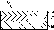
图2A-2C表示根据本发明的教导,光掩模坯件制备方法的不同阶段的截面图;和2A-2C illustrate cross-sectional views of various stages in a method of making a photomask blank in accordance with the teachings of the present invention; and
图3表示根据本发明的教导,用于在基底上沉积材料的离子束沉积装置;Figure 3 shows an ion beam deposition apparatus for depositing material on a substrate in accordance with the teachings of the present invention;
图4表示根据本发明的教导,通过传导对沉积在基底上的材料退火的样品装置;Figure 4 shows a sample device for annealing a material deposited on a substrate by conduction in accordance with the teachings of the present invention;
图5表示根据本发明的教导,通过对流对沉积在基底上的材料退火的样品装置;和Figure 5 shows a sample device for annealing material deposited on a substrate by convection in accordance with the teachings of the present invention; and
图6表示根据本发明的教导,通过辐射对沉积在基底上的材料退火的样品装置。Figure 6 shows a sample device for annealing a material deposited on a substrate by radiation in accordance with the teachings of the present invention.
发明详述Detailed description of the invention
通过参考图1到图6,可以对本发明的优选实施方案及其优点得到最佳理解,其中相似的数字代表相似和相应的部分。A preferred embodiment of the invention and its advantages are best understood by referring to Figures 1 through 6, wherein like numerals indicate like and corresponding parts.
图1为光掩模组件10的截面图。在该图示实施方案中,光掩模组件10包括与薄膜组件14结合的光掩模12。基底16和图案层18形成光掩模12,也称为掩模或光栅。光掩模12可以具有许多不同的尺寸和形状,包括但不限于圆形、长方形或方形。光掩模12也可以是任何一种光掩模类型,包括但不限于一次性掩模、五英寸光栅、六英寸光栅、九英寸光栅或任何其它可以用于将电路图案影像投影到半导体晶片上的适当尺寸的光栅。光掩模12也可以是双掩模(binary mask)、相移掩模(PSM)、光学邻近修正掩模(OPC)或任何其它适用于光刻术系统的掩模。FIG. 1 is a cross-sectional view of a
光掩模12包括在基底16上形成的图案层18,当图案层18曝光于光刻术系统中的电磁能时,会将图案投影到半导体晶片上(未在图中明确标出)。对于一些应用,基底16可以是一种透明材料,如石英、合成石英、熔凝硅石、氟化镁(MgF2)、氟化钙(CaF2)或任何其它可以透射至少75%的入射光的适当材料,其中该入射光的波长为约10纳米(nm)~约450nm。在一个可选实施方案中,基底16可以是一种反射材料,如硅或任何其它反射大于约50%的入射光的适当材料,其中该入射光的波长为约10nm~约450nm。Photomask 12 includes a patterned
图案层18可以是一种金属材料,如铬、氮化铬、金属-氧-碳-氮化物(M-O-C-N),其中该金属选自铬、钴、铁、锌、钼、铌、钽、钛、钨、铝、镁和硅,或任何其它能吸收波长在紫外线(UV)区域、深紫外线(DUV)区域、真空紫外线(VUV)区域和远紫外线(EUV)区域的电磁能的适当材料。在一个可选实施方案中,图案层18可以是一种部分透射材料,如化合物硅化钼(MoSi),其在UV、DUV、VUV和EUV区域具有约1%~约30%的透射率。The
框架20和薄膜22可以形成薄膜组件14。框架20通常由氧化铝形成,尽管它也可以由不锈钢、塑料或其它曝光于光刻术系统中的电磁能时不会降解或除气的适当材料形成。薄膜22可以是一种由以下材料形成的薄膜片,如硝化纤维素、乙酸纤维素、无定形含氟聚合物,如由E.I.du pont de Nemours and Company制备的TEFLONAF或由Asahi Glass制备的CYTOP,或是另一种对于位于UV、DUV、EUV和/或VUV区域的波长透明的适当薄膜。薄膜22可以通过传统技术,如旋转浇铸技术来制备。
薄膜22通过确保污染物与光掩模12保持确定距离来保护光掩模12免受污染物如尘土颗粒等的污染。这在光刻术系统中可能是极其重要的。在光刻法中,光掩模组件10曝光于由光刻术系统中的辐射能源产生的电磁能。该电磁能可以包括不同波长,如大约介于水银弧光灯的I-线和G-线之间的波长的光,或DUV、VUV或EUV光。在操作中,薄膜22被设计成允许很大比例的电磁能穿过它。薄膜22上收集到的污染物很可能偏离处理的晶片表面的焦点,因此,晶片上的曝光图像应当是清晰的。根据本发明的教导形成的薄膜22可以令人相当满意地应用于所有类型的电磁能,而不限于本申请中描述的光波。
光掩模12可以由光掩模坯件来制备。在一个实施方案中,光掩模坯件可以包括在基底上形成的至少一层不透明或部分透射的材料。这种材料可以通过物理汽相沉积法(PVD)、化学汽相沉积法(CVD)、离子束沉积法(IBD)或任何其它适当的沉积技术沉积到基底16上。在一种传统的沉积方法中,沉积材料中的固有应力可能使得基底的平直度降级,从而导致基底扭曲。基底的这种扭曲可能会在半导体制备方法中产生对准误差,从而可能损坏要制备的ICs的性能。在一个实施方案中,为降低沉积材料中的应力可以对基底施加热处理。这种热处理可以防止该基底扭曲,从而可以降低半导体制备方法中产生对准误差的可能性。另外,这种热处理还可以在基底和沉积工具的器壁之间产生一个温度梯度,从而使加热过的基底排斥掉污染物。
光掩模12可以使用一种标准光刻方法由热处理过的光掩模坯件形成。在光刻方法中,包含图案层18的数据的掩模图案文件可以由掩模布局文件产生。掩模布局文件可以包括代表集成电路中晶体管和电连接的多边形。当其在半导体晶片上被制备时,掩模布局文件中的多边形还可以代表集成电路中不同的层。例如,晶体管可以在具有扩散层和聚硅层的半导体晶片上形成。因此,该掩模布局文件可以包括一个或多个绘制在扩散层上的多边形和一个或多个绘制在聚硅层上的多边形。每一层上的多边形都可以转化成代表集成电路中一层的掩模图案文件。每一掩模图案文件都可以用于生产用于特定层的光掩模。
通过使用激光、电子束或X射线光刻术系统可以使所需图案在光掩模坯件的光刻胶层中成像。在一个实施方案中,激光光刻术系统使用发射具有约为364纳米(nm)的波长的光的氩离子激光。在可选实施方案中,激光光刻术系统使用发射具有约150nm~约300nm的波长的光的激光。光掩模12可以通过以下步骤制备:显影和蚀刻光刻胶层的曝光区域来产生图案,蚀刻图案层18未被光刻胶覆盖的部分,并除去未显影的光刻胶以在基底16上产生图案层18。The desired pattern can be imaged in the photoresist layer of the photomask blank by using a laser, electron beam, or X-ray lithography system. In one embodiment, the laser lithography system uses an argon ion laser that emits light having a wavelength of about 364 nanometers (nm). In an alternative embodiment, the laser lithography system uses a laser that emits light having a wavelength from about 150 nm to about 300 nm. The
图2A到2C表示在光掩模坯件制备方法不同阶段中的光掩模坯件30的截面图。在图2A中,提供了基底16。如上参考图1所述,基底16可以是一种透明材料,如石英、合成石英、熔凝硅石、氟化镁或氟化钙,或是一种反射材料,如硅。在图2B中,材料层32在基底16上形成。在一个实施方案中,光掩模坯件30可以被用于制备双光掩模。在该实施例中,材料层32可以是金属-氧-碳-氮化物(MaObCcNd),其中M是选自第IV、V和IV族的金属,并且b、c和d的值为0~1,并且a=1-(b+c+d),或是任何合适的材料,其中当该材料的厚度随其相关光学性能(如n和k)被调节时,该材料提供充足的光衰减并产生至少为2的光密度。材料层32可以以均匀、分级或多层的形式被沉积。2A to 2C show cross-sectional views of a photomask blank 30 at different stages in a photomask blank manufacturing method. In Figure 2A, a
在又一个实施方案中,光掩模坯件30可以用于制备相移掩模(PSM),包括但不限于交变PSM、衰减PSM和多色调PSM。在该实施例中,材料层32可以是均相或分级的MSixOyNz结构,其中M是选自第IV、V或VI族的金属,并且其中x+y+z=1,或是多层的M1OaNb/M2OcNd结构,其中M1是铝(Al)或硅(Si),M2是选自第IV、V或IV族的金属,a为0~1,b为0~1-a,c为0~1,并且d为0~1-c。这种多层结构可以是上述材料的组合从而使得至少一层对于曝光波长是不透明的,而另一层对于曝光波长是部分透射的。In yet another embodiment, photomask blank 30 may be used to make phase shift masks (PSMs), including but not limited to alternating PSMs, attenuating PSMs, and multi-tone PSMs. In this embodiment,
材料层32可以使用PVD、CVD、IBD或任何其它合适的沉积技术被沉积。如果使用IBD方法,与用其它溅射方法形成的材料相比,材料层32可能具有更高的密度。材料层32也可能具有高固有应力,这是因为沉积的颗粒或在溅射气体中使用的颗粒具有高能量。这些高能颗粒在基底16上生成可能具有高压缩应力的材料层32,这导致高应力层的产生。
在一个实施方案中,在沉积过程完成之前对基底16施加热处理可以降低材料层32中的应力。这种热处理可以通过辐射、对流、传导或任何其它在高于某一温度加热材料层32和/或基底16的技术来施加。为了达到大约300摄氏度(例如:大约600K)或更高的温度,这种处理可以连续或间歇施加。这种热处理的优点在于由于该热处理是在材料层32的沉积完成之前施加的,材料层32的光学性能是在沉积过程中决定的。In one embodiment, applying heat treatment to
在一个实施方案中,在沉积过程开始前对基底16施加该热处理。一旦基底16达到合适的温度,就可以将基底16放在沉积工具中。由于沉积工具的真空防止热量从基底16中散逸出去,基底16在沉积工具里保持该合适的温度。在另一实施方案中,可以在沉积过程中对基底16施加热处理。此外,该热处理也可以加热沉积在基底16上的材料。在又一实施方案中,可以在沉积过程开始前和沉积过程中都施加热处理以确保基底16保持合适的温度从而降低材料层32中的应力,并从材料层32中排斥掉不需要的颗粒。In one embodiment, this heat treatment is applied to
如下式所示,如果在沉积过程中对基底16和/或材料层32加热,光掩模12中的热应力(S热)可以用来抵消沉积薄膜的内在应力,因此减少了光掩模12的扭曲。As shown in the following equation, if the
S热=(αF-α)×EF×ΔTS heat = (α F -α) × E F × ΔT
αF和α分别是材料层32和基底16的平均膨胀系数,EF是材料层32的杨氏模量,而ΔT是基底16在沉积过程中的温度与测量时的温度之差。α F and α are the average coefficients of expansion of
如下式所示,材料层32中内在应力的降低增加了基底16的曲率半径(R),从而提高了光刻法中由光掩模坯件30形成的光掩模12的对准度。As shown in the following equation, the reduction in intrinsic stress in
其中σf是材料层32中的内在应力,Es是基底16的杨氏模量,νs是基底16的泊松比,df是材料层32的厚度,而ds是基底16的厚度。where σf is the intrinsic stress in the
基于上式,高于约300摄氏度(如约600K)的温度可以有效地降低材料层32中的应力,因此不必改变光掩模坯件30的任何光学性能就可以防止基底16的平直度降级。Based on the above equation, temperatures above about 300 degrees Celsius (eg, about 600K) can effectively reduce the stress in the
在沉积过程中施加的热处理也可能在沉积工具中产生热泳效应,这种效应在存在温度梯度时发生,该效应在被沉积以形成材料层32的颗粒和围绕气体分子的颗粒之间产生了不对称的相互作用。换言之,由该温度梯度导致的热泳效应会导致颗粒从热表面排斥出去,并被吸引到冷表面。通过对基底16加热,沉积室的器壁会比基底16的表面冷,多余的颗粒就会从基底16的表面被排斥出去。这种效应也可以抵消沉积过程中作用在颗粒上的其它的力,如重力和流体动量,并提供一个干净得多的沉积材料层。因此由于不需要的颗粒(如沉积工具中可能存在的污染物)从基底16和材料层32中被排出,材料层32可能具有低缺陷密度,The heat treatment applied during the deposition process may also create a thermophoretic effect in the deposition tool, which occurs when there is a temperature gradient, which creates a gap between the particles deposited to form the
如图2C所示,通过在材料层32上方形成光刻胶层34而完成光掩模坯件30。尽管图2B和2C表示具有单个材料层的光掩模坯件30,也可以形成两个或多个材料层,从而在前一层上形成后一层。然后光刻胶层34可以在绝大多数材料层的上面形成。然后可以用标准光刻法由光掩模坯件30制备光掩模12。Photomask blank 30 is completed by forming
图3表示可以用于沉积材料层32的离子束沉积(IBD)装置。在IBD方法中,等离子体放电,又称为离子枪或离子源,包含在室中,在离子枪出口,离子被施加到一系列栅极上的电势吸取并加速。这种IBD方法与其它利用溅射将材料从靶沉积到表面上的沉积方法相比有许多优点。首先,这种IBD方法在基底的沉积表面提供了一种更为洁净的方法(如不需要的颗粒更少),这是因为可以俘获并迁移带电颗粒到基底上的等离子体并不在基底上形成的材料层附近。其次,这种IBD方法是在一个较低的总气体压力下进行的,这就使得化学污染物的量减少。此外,这种IBD方法还具有独立地控制沉积流量、反应气体离子流量(电流)和能量的能力。最后,在双IBD方法中,可以调节材料靶、基底和离子枪之间的夹角以最优化薄膜均匀性和薄膜应力。FIG. 3 shows an ion beam deposition (IBD) apparatus that may be used to deposit
在单IBD方法中,被激发的离子束(通常被电子源中和)从沉积枪40射向位于靶支架(未明确示出)上的靶42。当从沉积枪40出来的轰击离子的能量高于特定靶材料的溅射阈能时,靶42上的材料就会被溅射。在一个实施方案中,该阈能可以为约50eV。In a single IBD approach, an excited ion beam (typically neutralized by an electron source) is directed from a
从沉积枪40出来的离子可以来自He、Ne、Ar、Kr、Xe等惰性气体源,尽管也可以使用O2、N2、CO2、F2、CH3或其组合等活泼气体。当这些离子来自惰性气体源时,源自靶42的材料被溅射并在基底16上沉积形成材料层32。当这些离子是由活泼气体源产生时,这些离子可能与来自靶42的材料结合,并且这种化学结合的产物被溅射并在基底16上沉积形成材料层32。在一个实施方案中,为了保持实际沉积速率(如高于0.1nm/min),轰击离子可以具有约200eV~约10KeV的能量,离子流量或电流可以高于约1013离子/cm2/s。室中的操作压力可以为约10-3~约10-5Torr。靶42可以由一种元素材料组成,如Si、Ti、Mo、Cr,或者该材料是一种化合物,如MoxSiy或SiO2,其中x为约0~约0.7,并且y=(1-x)。基底16位于与靶42的距离和方向能够最优化厚度和均匀性等薄膜性能并最小化应力的位置。The ions exiting the
在双离子束沉积方法中,除从沉积枪40出来的离子外,从辅助枪44出来的离子被电子源中和并射向基底16的表面。在操作中,辅助枪44提供流量可调节的低能离子(如低于大约100eV),该离子在基底16的表面与从靶42溅射出的原子反应以形成材料层32。从辅助枪44出来的离子可以源自活泼气体源如O2、N2、CO2、N2O、H2O、NH3、CF4、CHF3、F2、CH4或C2H2,或惰性气体如Ne、Ar、Kr、Xe或其组合。在一个实施方案中,来自辅助枪44的离子能量可能低于来自沉积枪40的离子能量。In the dual ion beam deposition method, in addition to ions from the
通常情况下,双IBD方法用于制备更加复杂的结构,该结构可能对形成用于曝光波长在DUV、VUV和EUV区域的光刻术的相移掩模有用,并且该结构生成大约180°的相移。例如,当基底16被来自辅助枪44的活泼氮轰击时,可以通过从各自的靶上交替沉积元素Si和Ti形成多层SiNx和TiNy,其中x为约1.0~约1.3,并且y为约1.0。然而,也可以通过使用约800V的束电压用单IBD方法沉积复杂结构。例如,单或双IBD方法都可以用于沉积材料,该材料包括但不限于Si3N4、TiN和多层化合物材料,如Si3N4/TiN、Ta2O5/SiO2、SiO2/TiN、Si3N4/SiO2或CrF3/AlF3。Typically, the dual IBD approach is used to fabricate more complex structures that may be useful for forming phase-shift masks for lithography with exposure wavelengths in the DUV, VUV, and EUV regions, and that generate approximately 180° phase shift. For example, when the
单或双IBD方法也可以用于沉积以具有交替光吸收层和光透射层的结构形式的材料层32。该吸收组分的特征在于对于低于约400nm的波长,消光系数k>0.1(如为约0.5~约3.5),而透射组分的特征在于对于低于约400nm的波长,消光系数k<<1.0。对于低于400nm的波长,吸收组分的折射率为约0.5~约3.0,而对于同样的波长,透射组分的折射率为约1.2~约3.5。Single or double IBD methods can also be used to deposit
材料层32的光透射组分可以选自合适的金属氧化物、金属氮化物或金属氟化物,以及光透射形式的碳。材料层32的基于氧化物的光透射组分可以选自光带隙能量高于约3eV的氧化物,包括但不限于硅、铝、锗、钽、铌、铪和锆的氧化物。材料层32的基于氮化物的光透射组分可以选自光带隙能量高于约3eV的氮化物材料,包括但不限于铝、硅、硼和碳的氮化物。材料层32的基于氟化物的光透射组分可以选自光带隙能量高于约3eV的氟化物等材料,包括但不限于第II族元素或镧系元素(如原子序数为57~71的元素)的氟化物。光透射碳可以包括具有金刚石结构的碳,有时指具有sp3C-C键的碳,又被称为类金刚石碳(DLC)。因为类金刚石碳的光学性能范围宽,其既能用作吸收层,又能用作透射层。一种或多种上述氧化物、氟化物、氮化物和DLC的组合也可以用单或双IBD方法沉积。The light transmissive component of
材料层32的光吸收组分可以选自元素金属、金属氮化物、氧化物和其任何组合。材料层32的基于氧化物的光吸收组分可以选自光带隙能低于材料层32透射组分的光带隙能的材料,包括但不限于第IIIB、IVB、VB和VIB元素的氧化物。材料层32的基于氮化物的光吸收组分可以选自光带隙能低于约3eV的材料,包括但不限于第IIIB、IVB、VB和VIB元素的氮化物。一种或多种金属、氧化物和氮化物的组合也可以用单或双IBD方法沉积。The light absorbing component of
材料层32的光吸收层和光透射层可以以周期性或非周期性排列的方式被离子束沉积。在一个实施方案中,薄膜的光吸收层和光透射层是以交替排列的方式被沉积的。The light-absorbing and light-transmitting layers of
单或双IBD方法也可以用于制备用于低于约400nm的光刻波长的双光掩模。例如,IBD方法可以用于沉积单层或多层的MOxCyNz,其中M选自铬、钼、钨、或钽或其任何组合,其中X为约0~约3.0,y为约0~约1.0,而z为约0~约2.0。在一个实施方案中,MOxCyNz材料的光密度可以大于约2个单位。Single or dual IBD methods can also be used to prepare dual photomasks for lithography wavelengths below about 400 nm. For example, the IBD method can be used to deposit monolayer or multilayer MOxCyNz , wherein M is selected from chromium, molybdenum, tungsten, or tantalum or any combination thereof, wherein x is about 0 to about 3.0, and y is about 0 to about 1.0, and z is from about 0 to about 2.0. In one embodiment, the MOxCyNz material can have an optical density greater than about 2 units.
概括而言,形成材料层32的IBD材料在晶体化学体系中可以归类于二元化合物类:AX、AX2、A2X、AmXz或其组合,其中m和z为整数,A代表阳离子,并且X代表阴离子。对两个位置(A,X),包括空位的部分化学取代是可能的,但要与保持化学中性一致。In general, the IBD material forming the
图4表示在基底16上沉积材料前或沉积过程中通过传导对材料层32退火的样品装置。通过夹紧放置在基底16相对面的屏蔽50可以将基底16固定在其所在的面上。安置在电热板54上的电阻线52可以与由计算机54控制的可调节的发电机(power generator)56联合。电热板54中的热电偶56可以将温度反馈到计算机54。为了降低材料层32中的应力,加热过程(如热处理)可以在材料层32在基底16上沉积之前或沉积过程中进行。FIG. 4 shows a sample device in which
图5表示在基底上沉积材料前或沉积过程中通过对流对材料层32退火的样品装置。沿着基底16的底表面周边放置的O-环60可以将基底16与对流装置分开。金属螺旋线62可以用于加热基底16下流动的气体63。在一个实施方案中,气体63可以是一种惰性气体,如He或Ar。在另一实施方案中,气体63可以是任何合适的气体,该气体提供良好的热转移性能,而又不会通过在沉积过程使用的气体中引入外来颗粒而污染材料层32。通过由计算机66控制的可调节阀门64,气体63可以放入对流装置中。然后气体63从基底16的下面通过并由排气口68排出。为降低被沉积材料中的内在应力,气体63在材料层32沉积前或沉积过程中对基底16加热。Figure 5 shows a sample device in which a
图6表示在基底上沉积材料前或沉积过程中通过辐射对材料层32退火的样品装置。可以将一个或多个提供红外或紫外区域辐射的灯70对准基底16,灯70可以包括非聚焦反射器72,其将辐射引向基底16的方向。在基底16上沉积材料的过程中或沉积前,可以打开灯70以对基底16施加热处理并降低材料层32中的应力。在一个实施方案中,这些灯可以对准基底16的前面(如材料层32形成的那面)。在另一实施方案中,如果这些灯使用红外区域的光,可以将这些灯对准基底16的背面。Figure 6 shows a sample device in which a
尽管本发明已经得到详细描述,应该理解对本发明进行不同的改变,取代和选择不会超出由后附的权利要求所限定的本发明的领域和范围。Although the present invention has been described in detail, it should be understood that various changes, substitutions and alternatives can be made therein without departing from the sphere and scope of the invention as defined by the appended claims.
Claims (27)
Applications Claiming Priority (4)
| Application Number | Priority Date | Filing Date | Title |
|---|---|---|---|
| US35153302P | 2002-01-24 | 2002-01-24 | |
| US60/351,533 | 2002-01-24 | ||
| US35569902P | 2002-02-07 | 2002-02-07 | |
| US60/355,699 | 2002-02-07 |
Publications (1)
| Publication Number | Publication Date |
|---|---|
| CN1653392A true CN1653392A (en) | 2005-08-10 |
Family
ID=27616809
Family Applications (1)
| Application Number | Title | Priority Date | Filing Date |
|---|---|---|---|
| CNA03802666XA Pending CN1653392A (en) | 2002-01-24 | 2003-01-24 | Photomask and method for manufacturing the same |
Country Status (5)
| Country | Link |
|---|---|
| US (1) | US7056623B2 (en) |
| JP (1) | JP2005516240A (en) |
| CN (1) | CN1653392A (en) |
| AU (1) | AU2003209383A1 (en) |
| WO (1) | WO2003062922A2 (en) |
Cited By (5)
| Publication number | Priority date | Publication date | Assignee | Title |
|---|---|---|---|---|
| CN1862376B (en) * | 2005-02-25 | 2011-05-04 | Hoya株式会社 | Mask blank transparent substrate manufacturing method, mask blank manufacturing method, and exposure mask manufacturing method |
| CN105045035A (en) * | 2014-04-24 | 2015-11-11 | 台湾积体电路制造股份有限公司 | Film structure and manufacturing method thereof |
| CN105629657A (en) * | 2014-11-26 | 2016-06-01 | 台湾积体电路制造股份有限公司 | EUV mask and manufacturing method by using the same |
| CN106842811A (en) * | 2017-03-20 | 2017-06-13 | 深圳市华星光电技术有限公司 | A kind of light shield and cleaning device |
| CN108227370A (en) * | 2016-12-14 | 2018-06-29 | 台湾积体电路制造股份有限公司 | Photomask and method of manufacturing the same |
Families Citing this family (8)
| Publication number | Priority date | Publication date | Assignee | Title |
|---|---|---|---|---|
| US7459095B2 (en) * | 2004-10-21 | 2008-12-02 | Corning Incorporated | Opaque chrome coating suitable for etching |
| JP2006133785A (en) * | 2004-11-08 | 2006-05-25 | Lg Micron Ltd | Halftone mask, method of manufacturing the same, and flat display manufactured thereby |
| JP4388467B2 (en) * | 2004-12-28 | 2009-12-24 | 信越化学工業株式会社 | Pellicle and pellicle frame for photolithography |
| JP2007212738A (en) * | 2006-02-09 | 2007-08-23 | Ulvac Seimaku Kk | Photomask blank and method of manufacturing same, and method of manufacturing photomask using photomask blank |
| CN103080840B (en) | 2010-06-25 | 2016-01-27 | Asml荷兰有限公司 | Lithographic apparatus and methods |
| TWI612369B (en) * | 2016-12-28 | 2018-01-21 | Micro Lithography Inc | EUV reticle inorganic protective film assembly manufacturing method |
| CN109143793B (en) * | 2018-09-06 | 2023-06-06 | 重庆科技学院 | A method of using an adjustable chip fixture |
| US11626286B1 (en) * | 2020-08-25 | 2023-04-11 | Rockwell Collins, Inc. | Custom photolithography masking via precision dispense process |
Family Cites Families (10)
| Publication number | Priority date | Publication date | Assignee | Title |
|---|---|---|---|---|
| US5372901A (en) * | 1992-08-05 | 1994-12-13 | Micron Technology, Inc. | Removable bandpass filter for microlithographic aligners |
| JPH07159974A (en) | 1993-12-09 | 1995-06-23 | Ryoden Semiconductor Syst Eng Kk | Pattern transfer mask and manufacturing method thereof |
| KR0138278B1 (en) | 1995-01-24 | 1998-04-27 | 김광호 | X-ray lithography mask and manufacturing method thereof |
| US5738909A (en) * | 1996-01-10 | 1998-04-14 | Micron Technology, Inc. | Method of forming high-integrity ultrathin oxides |
| US5792578A (en) * | 1997-01-13 | 1998-08-11 | Taiwan Semiconductor Manufacturing Company Ltd. | Method of forming multiple layer attenuating phase shifting masks |
| JP3368200B2 (en) * | 1998-02-26 | 2003-01-20 | シャープ株式会社 | Photomask making method and heat treatment apparatus |
| US6197454B1 (en) | 1998-12-29 | 2001-03-06 | Intel Corporation | Clean-enclosure window to protect photolithographic mask |
| JP2000231197A (en) | 1999-02-09 | 2000-08-22 | Mitsubishi Electric Corp | Resist pattern forming method, semiconductor device manufacturing method using the same, resist pattern forming apparatus and hot plate |
| US6242136B1 (en) * | 1999-02-12 | 2001-06-05 | Corning Incorporated | Vacuum ultraviolet transmitting silicon oxyfluoride lithography glass |
| JP3715189B2 (en) * | 2000-09-21 | 2005-11-09 | 株式会社ルネサステクノロジ | Phase shift mask |
-
2003
- 2003-01-24 CN CNA03802666XA patent/CN1653392A/en active Pending
- 2003-01-24 AU AU2003209383A patent/AU2003209383A1/en not_active Abandoned
- 2003-01-24 JP JP2003562722A patent/JP2005516240A/en active Pending
- 2003-01-24 US US10/350,876 patent/US7056623B2/en not_active Expired - Fee Related
- 2003-01-24 WO PCT/US2003/002281 patent/WO2003062922A2/en not_active Ceased
Cited By (8)
| Publication number | Priority date | Publication date | Assignee | Title |
|---|---|---|---|---|
| CN1862376B (en) * | 2005-02-25 | 2011-05-04 | Hoya株式会社 | Mask blank transparent substrate manufacturing method, mask blank manufacturing method, and exposure mask manufacturing method |
| CN105045035A (en) * | 2014-04-24 | 2015-11-11 | 台湾积体电路制造股份有限公司 | Film structure and manufacturing method thereof |
| CN114859653A (en) * | 2014-04-24 | 2022-08-05 | 台湾积体电路制造股份有限公司 | Protective film structure and manufacturing method thereof |
| CN105629657A (en) * | 2014-11-26 | 2016-06-01 | 台湾积体电路制造股份有限公司 | EUV mask and manufacturing method by using the same |
| CN105629657B (en) * | 2014-11-26 | 2019-11-22 | 台湾积体电路制造股份有限公司 | EUV mask and manufacturing method by using EUV mask |
| CN108227370A (en) * | 2016-12-14 | 2018-06-29 | 台湾积体电路制造股份有限公司 | Photomask and method of manufacturing the same |
| CN108227370B (en) * | 2016-12-14 | 2023-01-03 | 台湾积体电路制造股份有限公司 | Photomask and method of manufacturing the same |
| CN106842811A (en) * | 2017-03-20 | 2017-06-13 | 深圳市华星光电技术有限公司 | A kind of light shield and cleaning device |
Also Published As
| Publication number | Publication date |
|---|---|
| WO2003062922A2 (en) | 2003-07-31 |
| US7056623B2 (en) | 2006-06-06 |
| US20030138707A1 (en) | 2003-07-24 |
| WO2003062922A3 (en) | 2004-03-11 |
| JP2005516240A (en) | 2005-06-02 |
| AU2003209383A1 (en) | 2003-09-02 |
Similar Documents
| Publication | Publication Date | Title |
|---|---|---|
| US8663878B2 (en) | Mask and method for forming the same | |
| CN108227414B (en) | Mask structure and mask process method | |
| US9529250B2 (en) | EUV mask with ITO absorber to suppress out of band radiation | |
| US11988953B2 (en) | EUV masks to prevent carbon contamination | |
| CN1653392A (en) | Photomask and method for manufacturing the same | |
| CN1672099A (en) | Photomask and method for repairing defects | |
| US12535727B2 (en) | EUV lithography mask with a porous reflective multilayer structure | |
| EP1777588B1 (en) | Fabrication method of photomask-blank | |
| US11982936B2 (en) | Photomask and method of fabricating a photomask | |
| WO2004049063A2 (en) | Photomask and method for creating a protective layer on the same | |
| CN1846174A (en) | Photomask and method for maintaining optical properties of the same | |
| US6869734B1 (en) | EUV reflective mask having a carbon film and a method of making such a mask | |
| US20240069431A1 (en) | Method of manufacturing photo masks | |
| US8916482B2 (en) | Method of making a lithography mask | |
| TW202009982A (en) | Mask and method for manufacturing the same and method for patterning a layer | |
| US6852455B1 (en) | Amorphous carbon absorber/shifter film for attenuated phase shift mask | |
| CN1742232A (en) | Photomask and method of manufacturing protective layer thereon | |
| JP4603983B2 (en) | Photomask blank and photomask blank manufacturing method | |
| TW557409B (en) | Photomask and method for manufacturing the same | |
| WO2022153657A1 (en) | Reflective photomask blank and reflective photomask | |
| JPH046558A (en) | Method for forming phase shifting mask |
Legal Events
| Date | Code | Title | Description |
|---|---|---|---|
| C06 | Publication | ||
| PB01 | Publication | ||
| C10 | Entry into substantive examination | ||
| SE01 | Entry into force of request for substantive examination | ||
| C02 | Deemed withdrawal of patent application after publication (patent law 2001) | ||
| WD01 | Invention patent application deemed withdrawn after publication |