CN1668942A - Optical substrate and manufacturing method thereof - Google Patents
Optical substrate and manufacturing method thereof Download PDFInfo
- Publication number
- CN1668942A CN1668942A CNA038166631A CN03816663A CN1668942A CN 1668942 A CN1668942 A CN 1668942A CN A038166631 A CNA038166631 A CN A038166631A CN 03816663 A CN03816663 A CN 03816663A CN 1668942 A CN1668942 A CN 1668942A
- Authority
- CN
- China
- Prior art keywords
- function
- optical substrate
- functions
- window
- surface structure
- Prior art date
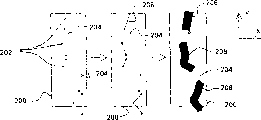
- Legal status (The legal status is an assumption and is not a legal conclusion. Google has not performed a legal analysis and makes no representation as to the accuracy of the status listed.)
- Granted
Links
Images




Classifications
-
- G—PHYSICS
- G02—OPTICS
- G02B—OPTICAL ELEMENTS, SYSTEMS OR APPARATUS
- G02B5/00—Optical elements other than lenses
- G02B5/02—Diffusing elements; Afocal elements
- G02B5/0205—Diffusing elements; Afocal elements characterised by the diffusing properties
- G02B5/021—Diffusing elements; Afocal elements characterised by the diffusing properties the diffusion taking place at the element's surface, e.g. by means of surface roughening or microprismatic structures
- G02B5/0221—Diffusing elements; Afocal elements characterised by the diffusing properties the diffusion taking place at the element's surface, e.g. by means of surface roughening or microprismatic structures the surface having an irregular structure
-
- G—PHYSICS
- G02—OPTICS
- G02B—OPTICAL ELEMENTS, SYSTEMS OR APPARATUS
- G02B5/00—Optical elements other than lenses
- G02B5/02—Diffusing elements; Afocal elements
-
- G—PHYSICS
- G02—OPTICS
- G02B—OPTICAL ELEMENTS, SYSTEMS OR APPARATUS
- G02B13/00—Optical objectives specially designed for the purposes specified below
- G02B13/20—Soft-focus objectives
-
- G—PHYSICS
- G02—OPTICS
- G02B—OPTICAL ELEMENTS, SYSTEMS OR APPARATUS
- G02B5/00—Optical elements other than lenses
-
- G—PHYSICS
- G02—OPTICS
- G02B—OPTICAL ELEMENTS, SYSTEMS OR APPARATUS
- G02B5/00—Optical elements other than lenses
- G02B5/02—Diffusing elements; Afocal elements
- G02B5/0205—Diffusing elements; Afocal elements characterised by the diffusing properties
- G02B5/021—Diffusing elements; Afocal elements characterised by the diffusing properties the diffusion taking place at the element's surface, e.g. by means of surface roughening or microprismatic structures
- G02B5/0231—Diffusing elements; Afocal elements characterised by the diffusing properties the diffusion taking place at the element's surface, e.g. by means of surface roughening or microprismatic structures the surface having microprismatic or micropyramidal shape
-
- G—PHYSICS
- G02—OPTICS
- G02B—OPTICAL ELEMENTS, SYSTEMS OR APPARATUS
- G02B6/00—Light guides; Structural details of arrangements comprising light guides and other optical elements, e.g. couplings
- G02B6/0001—Light guides; Structural details of arrangements comprising light guides and other optical elements, e.g. couplings specially adapted for lighting devices or systems
- G02B6/0011—Light guides; Structural details of arrangements comprising light guides and other optical elements, e.g. couplings specially adapted for lighting devices or systems the light guides being planar or of plate-like form
- G02B6/0033—Means for improving the coupling-out of light from the light guide
- G02B6/005—Means for improving the coupling-out of light from the light guide provided by one optical element, or plurality thereof, placed on the light output side of the light guide
- G02B6/0053—Prismatic sheet or layer; Brightness enhancement element, sheet or layer
-
- G—PHYSICS
- G02—OPTICS
- G02B—OPTICAL ELEMENTS, SYSTEMS OR APPARATUS
- G02B6/00—Light guides; Structural details of arrangements comprising light guides and other optical elements, e.g. couplings
- G02B6/0001—Light guides; Structural details of arrangements comprising light guides and other optical elements, e.g. couplings specially adapted for lighting devices or systems
- G02B6/0011—Light guides; Structural details of arrangements comprising light guides and other optical elements, e.g. couplings specially adapted for lighting devices or systems the light guides being planar or of plate-like form
- G02B6/0033—Means for improving the coupling-out of light from the light guide
- G02B6/005—Means for improving the coupling-out of light from the light guide provided by one optical element, or plurality thereof, placed on the light output side of the light guide
- G02B6/0051—Diffusing sheet or layer
Landscapes
- Physics & Mathematics (AREA)
- General Physics & Mathematics (AREA)
- Optics & Photonics (AREA)
- Optical Elements Other Than Lenses (AREA)
- Liquid Crystal (AREA)
- Overhead Projectors And Projection Screens (AREA)
- Planar Illumination Modules (AREA)
Abstract
Description
技术领域technical field
本发明涉及光学基底,以及更具体地涉及具有执行至少两种功能的表面的光学基底。The present invention relates to optical substrates, and more particularly to optical substrates having surfaces that perform at least two functions.
背景技术Background technique
在背光计算机显示器(backlight computer display)或其它系统中,薄膜通常用于引导光。例如,在背光显示器中,亮度增强膜采用棱镜结构,沿着观察轴(即,垂直于显示器)引导光,这增强了显示器的使用者观察到的光的亮度以及使得该系统使用较少功率就能产生所需程度的轴上(on-axis)照明。用于改变光方向的薄膜也可使用在多种其它光学设计中,例如用于投影显示仪、交通信号灯和照明标志中。Films are often used to guide light in backlight computer displays or other systems. For example, in backlit displays, the brightness enhancement film employs a prismatic structure that directs light along the viewing axis (i.e., perpendicular to the display), which enhances the brightness of the light seen by a user of the display and allows the system to operate using less power. The desired degree of on-axis illumination can be produced. Films used to redirect light can also be used in a variety of other optical designs, such as in projection displays, traffic lights, and illuminated signs.
背光显示器和其它系统使用下述膜的层,堆叠和布置所述膜以使其棱柱曲面互相垂直并夹在称为散射体(diffuser)的其它光学膜之间。散射体具有高度不规则表面。Backlit displays and other systems use layers of films that are stacked and arranged so that their prismatic surfaces are perpendicular to each other and sandwiched between other optical films called diffusers. Scatterers have highly irregular surfaces.
发明内容Contents of the invention
本发明特征在于多功能光学基底及其制造方法。在本发明的一个方面,光学基底包括以例如相关函数R(x,y)等函数为特征的三维表面,所述相关函数R(x,y)在约1厘米或更小的相关长度lc内具有小于其初始值R的约37%(1/e)的值。该三维表面是由第一表面结构函数定义的,该第一表面结构函数由第二随机函数或至少是伪随机函数调制。第一表面结构函数的性质从第一输入光束中产生了镜像分量(specular component),以及该光方向改变性能保留在该三维表面内。通常,伪随机函数是一种信号,其调制第一表面结构函数的频率、高度、最大角(peak angle)或相的任意组合。定义一个窗口,并在该窗口内随机选择点,从而创建连接随机选择的点的调制通道。定义一个主函数并沿着调制通道产生表面函数,表面函数在主函数内连续位置处与该主函数重复结合。所得的基底三维表面不仅保持第一表面结构函数的光方向改变特性,而且可散射光以减少,例如莫尔条纹假象(Moireartifact)。The invention features a multifunctional optical substrate and a method of manufacturing the same. In one aspect of the invention, an optical substrate comprises a three-dimensional surface characterized by a function such as a correlation function R(x,y) at a correlation length lc of about 1 cm or less In has a value less than about 37% (1/e) of its initial value R. The three-dimensional surface is defined by a first surface structure function modulated by a second random function or at least a pseudorandom function. The properties of the first surface structure function produce a specular component from the first input beam, and the light redirecting properties are preserved within the three-dimensional surface. Typically, the pseudorandom function is a signal that modulates any combination of frequency, height, peak angle, or phase of the first surface structure function. Defines a window and randomly selects points within the window, creating a modulation channel connecting the randomly selected points. A main function is defined and a surface function is generated along the modulation channel, the surface function being repeatedly combined with the main function at successive positions within the main function. The obtained three-dimensional surface of the substrate not only maintains the light direction changing property of the first surface structure function, but also scatters light to reduce, for example, Moire artifacts.
在本发明的另一个方面,光学基底被涂布到在背光面板导光板(backlight panel light guide)中用于亮度增强的膜的一侧或多侧。在亮度增强应用中,该光学基底也产生至少约30%的轴上亮度增加。此外,三维表面产生光的散射镜像分量,其具有约0.1-60°之间的半功率角(power half angle)。In another aspect of the invention, the optical substrate is coated to one or more sides of a film for brightness enhancement in a backlight panel light guide. In brightness enhancement applications, the optical substrate also produces an on-axis brightness increase of at least about 30%. Furthermore, the three-dimensional surface produces a diffuse mirror component of light with a power half angle between about 0.1-60°.
附图说明Description of drawings
图1是现有技术膜的截面图,其中使用一系列棱镜结构来改变光方向。Figure 1 is a cross-sectional view of a prior art film in which a series of prismatic structures are used to redirect light.
图2是本发明一个实施方案的光学基底的顶视图。Figure 2 is a top view of an optical substrate according to one embodiment of the present invention.
图3是本发明另一实施方案的第二光学基底的顶视图。Figure 3 is a top view of a second optical substrate according to another embodiment of the present invention.
图4是图3的光学基底的透视图。FIG. 4 is a perspective view of the optical substrate of FIG. 3 .
图5是显示本发明一个实施方案的光学基底的三个截面图的图示。Fig. 5 is a diagram showing three cross-sectional views of an optical substrate according to an embodiment of the present invention.
图6是本发明一个实施方案的光学基底的截面图,其显示了光束的改向和散射。Figure 6 is a cross-sectional view of an optical substrate showing light beam redirection and scattering according to one embodiment of the present invention.
图7是平板显示器的透视图。Fig. 7 is a perspective view of a flat panel display.
图8是单波形的顶视图,其可用于对本发明一个实施方案的光学基底建立模型。Figure 8 is a top view of a single waveform that can be used to model an optical substrate according to one embodiment of the present invention.
图9是显示在图8所示的波形长度方向上相的变化的图。FIG. 9 is a graph showing changes in phase in the lengthwise direction of the waveform shown in FIG. 8 .
图10是显示在图8所示的波形长度方向上最大角的变化的图。FIG. 10 is a graph showing changes in the maximum angle in the length direction of the waveform shown in FIG. 8 .
图11是在进行将调制的波形结构放置在主图像(master image)上的第一迭代后形成的表面结构。Figure 11 is the surface structure formed after the first iteration of placing the modulated waveform structure on the master image.
图12是在将调制的波形结构放置在图11的结构上的第二迭代后形成的表面结构。FIG. 12 is a surface structure formed after a second iteration of placing a modulated waveform structure on the structure of FIG. 11 .
图13是随机化的基底表面的图示。Figure 13 is an illustration of a randomized substrate surface.
图14是在产生调制波形的窗口内随机分布的控制点的示意图。Fig. 14 is a schematic diagram of randomly distributed control points within the window in which the modulated waveform is generated.
图15是将图14的调制波形施加至主函数的图示。FIG. 15 is a graphical representation of the modulation waveform of FIG. 14 applied to the main function.
图16是产生随机基底表面的方法的流程图。16 is a flowchart of a method of generating a random substrate surface.
图17是在晶片上平铺(tile)随机基底表面的图示。Figure 17 is an illustration of tiling a random substrate surface on a wafer.
图18是40微米间距棱镜阵列的高度图(height map)的顶视图。Figure 18 is a top view of a height map of a 40 micron pitch prism array.
图19是图18的40微米间距棱镜阵列的水平部分的归一化自相关函数。FIG. 19 is a normalized autocorrelation function for the horizontal portion of the 40 micron pitch prism array of FIG. 18 .
图20是图18的40微米间距棱镜阵列与50微米间距参照棱镜的莫尔条纹干涉图(Moire map)的顶视图。20 is a top view of a Moire map of the 40 micron pitch prism array of FIG. 18 and a 50 micron pitch reference prism.
图21是图20的莫尔条纹干涉图的分布。FIG. 21 is a distribution of the moiré fringe interferogram of FIG. 20 .
图22是在棱镜中心水平位置随机化的图18的40微米间距棱镜阵列的高度图的顶视图。22 is a top view of a height map of the 40 micron pitch prism array of FIG. 18 randomized at the horizontal position of the prism centers.
图23是图22的高度图的水平部分的归一化自相关函数。FIG. 23 is a normalized autocorrelation function for the horizontal portion of the height map of FIG. 22 .
图24是图22的高度图的莫尔条纹干涉图的顶视图Figure 24 is a top view of the Moiré fringe interferogram of the height map of Figure 22
图25是图24的莫尔条纹干涉图的分布。FIG. 25 is a distribution of the moiré fringe interferogram of FIG. 24 .
图26是在棱镜中心水平位置满循环(full cycle)随机化的图18的40微米间距棱镜阵列的高度图的顶视图,所述棱镜中心具有叠加相调制的棱镜波形。26 is a top view of a height map of the 40 micron pitch prism array of FIG. 18 randomized full cycle at the horizontal position of the prism centers with superimposed phase modulated prism waveforms.
图27是图26的高度图的水平部分的归一化自相关函数。FIG. 27 is a normalized autocorrelation function for the horizontal portion of the height map of FIG. 26 .
图28是图26的40微米间距棱镜阵列的高度图的莫尔条纹干涉图的顶视图。28 is a top view of a Moiré fringe interferogram of the height map of the 40 micron pitch prism array of FIG. 26 .
图29是图28的莫尔条纹干涉图的分布。FIG. 29 is a distribution of the moiré fringe interferogram of FIG. 28 .
图30是40微米间距棱镜阵列和44微米间距棱镜阵列的莫尔条纹干涉图的顶视图。Figure 30 is a top view of the Moiré fringe interferograms for a 40 micron pitch prism array and a 44 micron pitch prism array.
图31是在棱镜中心水平位置随机化的40微米间距棱镜阵列和44微米间距棱镜阵列的莫尔条纹干涉图的顶视图。Fig. 31 is a top view of Moiré fringe interferograms for a 40 micron pitch prism array and a 44 micron pitch prism array randomized at the horizontal position of the prism centers.
图32是图26的高度图相对于44微米间距参照棱镜阵列的莫尔条纹干涉图的顶视图。Figure 32 is a top view of the Moiré fringe interferogram of the height map of Figure 26 versus a 44 micron pitch reference prism array.
图33是图26的40微米间距棱镜阵列的高度图的垂直自相关图。33 is a vertical autocorrelation plot of the height map of the 40 micron pitch prism array of FIG. 26 .
图34是图22的40微米间距棱镜阵列的高度图的垂直自相关图。34 is a vertical autocorrelation plot of the height map of the 40 micron pitch prism array of FIG. 22 .
图35是由随机函数在幅度上调制的载波c(x)的图示。Figure 35 is a graphical representation of a carrier c(x) modulated in amplitude by a random function.
图36是由随机函数在相上调制的载波c(x)的图示。Figure 36 is a diagram of a carrier c(x) modulated in phase by a random function.
图37是由随机函数在频率上调制的载波c(x)的第一图示。Figure 37 is a first illustration of a carrier c(x) modulated in frequency by a random function.
图38是由随机函数在频率上调制的载波c(x)的第二图示。Figure 38 is a second illustration of a carrier c(x) modulated in frequency by a random function.
图39是使用承载形函数(carrier function)和噪声函数调制频率和幅度的图示。Figure 39 is a graphical representation of frequency and amplitude modulation using a carrier function and a noise function.
图40是骨架屏蔽函数(skeleton mask function)的图像。Figure 40 is an image of a skeleton mask function.
图41是背光显示器件的剖视图。Fig. 41 is a cross-sectional view of a backlight display device.
具体实施方式Detailed ways
本发明的实施方案提供使用光学基底的表面改向和散射光的光学基底。该基底包括由用于改变光方向的第一表面结构函数和用于散射光的第二表面结构函数所定义的表面。这两个表面函数的结合生成了能改变光方向和散射光的单个三维表面。Embodiments of the present invention provide optical substrates that redirect and scatter light using the surface of the optical substrate. The substrate includes a surface defined by a first surface structure function for redirecting light and a second surface structure function for scattering light. The combination of these two surface functions creates a single 3D surface that redirects and scatters light.
以下将参考用于背光显示器等的亮度增强膜,描述基底的实施方案。然而,光学基底也可用于多种其它应用中。Embodiments of substrates will be described below with reference to brightness enhancement films for backlit displays and the like. However, optical substrates can also be used in a variety of other applications.
图1描述了现有技术膜的横截面,其中使用一系列棱镜结构10来改变光方向。在背光显示器中,光进入表面20并从表面30逸出。在图1的膜中,将与光进入表面(light-entering surface)20具有0°入射角的光束A引导离开棱镜结构10,以及基本上反射回至输入。通过棱镜结构10改变具有θ入射角的第二光束B的方向,以使其透射通过光逸出表面(light-exitingsurface)30以及基本上垂直于光进入表面20逸出。其它光束(未显示)将以其它角度改变方向或反射。这种膜的整体统计性质的特征在于如光学增益和观察角等参数。Figure 1 depicts a cross-section of a prior art film in which a series of
在该现有技术的膜中,可将表面30描述成一个函数。如果表面30相对于表面20的高度是z,以及穿过纸张和垂直于纸张的坐标分别是x,y,则表面30可定义成函数z=f(x,y)。在这种情况下,f(x)是相对于表面20具有恒定偏移的重复三角波形或锯齿形。在这种情况下,定义表面30的函数具有以上概述的同时改变光方向和反射光的特殊几何形状。In this prior art film, the
图2是本发明第一实施方案的光学基底的顶视图。图2的实施方案显示了长(l)约2000微米和宽(w)约2000微米的基底40的一部分。图3是尺寸约为500微米×500微米的一部分基底42的实施方案的顶视图,图4是图3的一部分光学基底42的透视图。图3和4的实施方案的三维表面比图2的三维表面更不规则。通常,图2-4中所示的基底在其光逸出表面上具有不规则的三维表面结构。由于它的几何形状,不规则的三维表面结构改变光的方向,产生输出镜像分量,同时散射光并具有小的相关长度lc。因为该基底的实施方案可在单个表面上改变光方向并散射光,所以可在一些应用中除去单独的散射表面。Fig. 2 is a top view of an optical substrate according to a first embodiment of the present invention. The embodiment of Figure 2 shows a portion of a
图2-4所示的基底具有不规则的三维表面。然而,该不规则的表面不能容易地用公知的数学函数来定义,如图1的光逸出表面30的情况。相反,该表面函数更好地被定义为通过第二表面函数调制第一表面结构函数的结果,以及在一些情况下通过采取这样的调制函数和将它们与类似形成的其它函数叠加。例如,该第一函数可与图1的光逸出表面30所定义的函数类似。第一函数也可为单棱镜的函数。第二函数可为高度、相、频率或最大角的伪随机函数。此外,通过用第二函数调制第一函数可完成该结合,以使基底40的所得函数z=f(x,y)具有沿着基底40的“I”方向伪随机变化的高度、相、频率或最大角(图2)。第一函数提供了改变光方向或反射光的几何特性,以及第二函数提供了散射改变方向的光或反射的光的几何特性。如以下将要讨论的,可替换其它函数以及其它参数可能是相关的(例如,实体的相)。如果使用棱柱表面函数作为第一函数,则第一表面函数的高度h、宽度s和最大角α可根据基底的预期用途而改变。此外,第一表面函数不必须为图1所示的对称结构。The substrates shown in Figures 2-4 have irregular three-dimensional surfaces. However, this irregular surface cannot be easily defined by well-known mathematical functions, as is the case with the
在一个实施方案中,通过第二表面结构函数调制第一表面结构函数的相、频率、最大角或高度。第二表面结构函数定义调制的类型,以在基底40的光逸出表面41(图2)上产生膜的三维表面。因而,通过这两个表面结构函数的结合定义基底40的光逸出表面41的表面高度。例如,可沿着基底40的长度l调制一个或多个第一表面结构函数(例如棱镜)的峰的高度。可沿着基底40的长度l在随机或固定间隔内的某些极限之间随机或伪随机地调制该高度。就最好的理解,术语“随机”是指真正随机或者通过人为方法而产生的尽可能程度的随机,例如伪随机。在另一个实施例中,可沿着基底40的长度l在某些极限之间至少伪随机地调制一个或多个第一表面结构函数的相,即沿着基底40的宽度w的水平位置。在另一实施例中,可沿着基底40的长度l调制第一表面结构函数的最大角。因此,可使用调制技术组合来创建基底40的三维表面,以使单个三维表面改变光方向及散射光。将在下文中更详细地介绍用于产生图2所示的基底40的具体调制技术。In one embodiment, the phase, frequency, maximum angle or height of the first surface structure function is modulated by the second surface structure function. The second surface structure function defines the type of modulation to create a three-dimensional surface of the film on the light-exit surface 41 of the substrate 40 (FIG. 2). Thus, the surface height of the light-exit surface 41 of the
图5是沿着图2的长度l在不同位置处基底40的三个横截面的图示。第一横截面50,例如取自沿着图2的l方向400微米位置处,可延长部分基底40的宽度w(具体地,在w方向上约200-500微米之间)。第二横截面52可取自,例如沿着图2的l方向在800微米位置处,以及第三横截面54可取自,例如沿着图2的l方向在约1400微米位置处。图5中纵轴是指仅显示基底40表面的高度变化量,而非基底40的实际高度。图5中的横轴显示沿着图2中w方向上的水平位置。从图5中的横截面可知,在基底40的具体横截面50、52和54处调制的锯齿形函数继续存在。因为这些结构的相已经被调制,然而,各横截面50、52和54均具有与其它横截面50、52和54不对齐的峰56。这也可从图2的顶视图中清楚可见,在图2中延续基底40长度l的调制表面函数46易于摇摆、改向、合并或分叉、以及交叉,从而使得没有离散的元件。在图5中,锯齿形函数的最大角58为约90°。尽管图5没有显示锯齿形函数的调制最大角,但是对给定的光学元件46而言,这些最大角也可沿着图2的通常长度方向l从一个峰变化到下一个峰。该峰是w方向上所得表面横截面上的局部高度最大值。FIG. 5 is an illustration of three cross-sections of the
即使在调制第一表面结构函数,以产生基底40的三维表面之后,从输入光束中产生输出镜像分量的第一表面结构函数的特性大部分仍然保留在所得的三维表面中。通过改变施加至第一表面结构函数的幅度和/或空间频率调制,可调节镜面性能或光改变性能的量。例如,减少施加至第一表面结构函数的调制量可增加镜像性能。相反,施加至第一表面结构函数的调制量的增加降低了镜像性能,但增加了散射。类似地,施加至第一表面结构函数的调制量的减少也降低了基底的散射性能,以及施加至第一表面结构函数的调制量的增加增加了基底的散射性能。Even after the first surface structure function is modulated to create the three-dimensional surface of
图6显示了可用于亮度增强应用的光学基底100的示例性实施方案的改向和散射性质。为清楚说明,在图6中没有显示图2的不规则三维表面41,但是如果显示未具有从约100毫米至约1纳米的特征表面尺寸的光逸出表面102,则在图6中将会显示图2的不规则三维表面41。与基底100具有0°入射角θ的第一光束138被光逸出表面102朝着输入方向引导返回。该光不仅被引导返回,而且也被散射,从而不是形成了单个输出光束,而是形成了由光线136和134构成的第一散射椭圆。例如,散射光可存在于光线136和134构成的椭圆内,从而形成实心椭圆。基底100引导入射角为θ的第二输入光束124,以使其作为逸出光束128透射通过光逸出表面102并且改变方向,从而大致以垂直于基底100而逸出。光束128也被光逸出表面102散射,以形成第二散射椭圆。第二散射椭圆是通过128和光线130或132之间的半功率角Φ形成的。半功率角Φ可用作基底100散射特性的一个度量,其可在约0.1和60°之间变化。在其它实施方案中,通过改变调制的类型和/或量,半功率角Φ可在约1和5°之间。图6显示至少一个输出光束130和132被基底100改变方向,并偏离其输入的入射角θ。Figure 6 shows the redirecting and scattering properties of an exemplary embodiment of an
图6中基底100的散射特性可在大范围内变化。例如,在一个实施方案中形成的散射椭圆可为对称的圆锥。在其它的实施方案中,散射可根本不对称或者仅有很少对称。可控制随机调制,以不同地影响w和l方向上的散射,即幅度、带宽,以及调制参数可施加到沿w或l任一方向的一维,或者沿w、l方向上的具有不同参数的二维。可以使用其它坐标,相对于第一表面函数改变调制函数的取向,包括其它旋转或变换的直角坐标几何结构,例如圆柱、球形或普通扭曲坐标系统(generally warped coordinate system)。当不对称的图案是所需的时候,可使用这些系统。The scattering properties of the
基底的光引导特性也可在大范围内变化。参考图7,如果使用具有灯108和下反射面109的背面发光单元的导光板106,则基底112和114可显著增强亮度,同时也散射光。在亮度增强实施方案中,当轴上观察时,基底112和114可增强亮度约30%至约300%。由于莫尔干涉效应(Moire effect)的原因,不能使用现有技术的线性棱镜阵列以及具有随机棱镜阵列的亮度增强膜,或者平行地使用这些阵列不是理想的。在本发明中,可使用两个基底,基底相互之间的角度可为在十字(直角)和平行之间的任意角度,这是因为没有莫尔效应。这允许在光输出图案中有更多灵活性。在其它的实施方案中,基底增加轴上亮度至少约50%,以及可能多至约200%。在亮度增强实施方案中,可将两个基底112和114布置成相互之间为直角,以改变来自不同方向的输入光束的方向并散射。因为散射性能是基底112和114的构成部分,所以不需要使用单独的散射基底来消除由基底112和114所引起的莫尔条纹假象,尽管在本发明范围内可由于其它原因使用散射基底。The light-guiding properties of the substrate can also vary over a wide range. Referring to FIG. 7, if the light guide plate 106 of the backside light-emitting unit having the lamp 108 and the lower reflective surface 109 is used, the substrates 112 and 114 can significantly enhance brightness while also diffusing light. In a brightness enhancement embodiment, substrates 112 and 114 may enhance brightness by about 30% to about 300% when viewed on-axis. Due to the Moire effect, prior art linear prism arrays as well as brightness enhancement films with random prism arrays cannot be used, or it is not ideal to use these arrays in parallel. In the present invention, two substrates can be used, and the angle of the substrates to each other can be any angle between cross (right angle) and parallel, because there is no moiré effect. This allows for more flexibility in the light output pattern. In other embodiments, the substrate increases on-axis brightness by at least about 50%, and possibly as much as about 200%. In a brightness enhancement embodiment, the two substrates 112 and 114 may be arranged at right angles to each other to redirect and scatter incoming light beams from different directions. Because the scattering properties are an integral part of substrates 112 and 114, it is not necessary to use separate scattering substrates to eliminate the moiré artifacts caused by substrates 112 and 114, although scattering substrates may be used for other reasons within the scope of the present invention.
现有技术的图7显示散射体116和118。散射体118散射莫尔条纹假象,该莫尔条纹假象来自于由基底112和114的任何固有规则性所引起的干涉。由于导光板106下侧120上的抽出器图案的规则性和LCD面板122的规则性的原因,散射体116散射莫尔条纹假象。常规亮度增强膜112和114可用本发明代替,从而可能消除散射体118和116。Prior art FIG. 7 shows scatterers 116 and 118 . Scatterers 118 scatter moiré artifacts that result from interference caused by any inherent regularity of substrates 112 and 114 . Due to the regularity of the extractor pattern on the underside 120 of the light guide plate 106 and the regularity of the LCD panel 122 , the scatterers 116 scatter moiré artifacts. Conventional brightness enhancement films 112 and 114 can be replaced by the present invention, thereby potentially eliminating scatterers 118 and 116 .
基底112和114的散射特性减少或消除了由多种普通的光引导膜(例如,图1所示的)所引起的莫尔条纹假象。因此,结合这些基底的示例性膜可在一个面上改变光方向并散射光,从而减少或消除莫尔条纹假象。The scattering properties of substrates 112 and 114 reduce or eliminate moiré artifacts caused by many common light directing films (eg, that shown in FIG. 1 ). Accordingly, exemplary films incorporating these substrates can redirect and scatter light on one side, thereby reducing or eliminating moiré artifacts.
自相关函数R(x,y)是在表面度量衡学中使用的表面随机性的度量。然而,在确定的相关长度lc内,自相关函数R(x,y)的值降低至其初始值的一小部分。例如,1.0的自相关值将被认为是高度或者完美相关的表面。相关长度lc是自相关函数的值是其初始值的确定分数时的长度。典型地,相关长度基于自相关函数的初始值的1/e或者37%。较大的相关长度是指该表面比相关长度较小的表面的随机性小。自相关函数的更详细的讨论提供在DavidJ.Whitehouse,Handbook of Surface Metrology,IOP Publishing Ltd.(1994),p.49-58中。The autocorrelation function R(x,y) is a measure of surface randomness used in surface metrology. However, within a determined correlation length lc , the value of the autocorrelation function R(x,y) decreases to a fraction of its initial value. For example, an autocorrelation value of 1.0 would be considered a highly or perfectly correlated surface. The correlation length l c is the length at which the value of the autocorrelation function is a certain fraction of its initial value. Typically, the correlation length is based on 1/e or 37% of the initial value of the autocorrelation function. A larger correlation length means that the surface is less random than a surface with a smaller correlation length. A more detailed discussion of autocorrelation functions is provided in David J. Whitehouse, Handbook of Surface Metrology, IOP Publishing Ltd. (1994), p.49-58.
在本发明的一些实施方案中,光学基底100的三维表面的自相关函数的值在约1厘米或更小的相关长度内降至小于或等于其初始值的1/e。在其它实施方案中,自相关函数的值在约0.5厘米或更小内降至其初始值的1/e。对图2和6所示的基底40和100的实施方案而言,沿着长度l方向的自相关函数的值在约200微米或更小内降至小于或等于其初始值的1/e。对图2和6的相同实施方案而言,沿着宽度w方向的自相关函数的值在约11微米或更小内降至小于或等于其初始值的1/e。In some embodiments of the invention, the value of the autocorrelation function of the three-dimensional surface of
相关长度与莫尔条纹假象的减少有关。应当注意,较小的相关长度表示比较大的相关长度具有更多随机表面,以及较小的相关长度也与更多的散射和莫尔条纹假象的减少有关。因为如低相关长度所表明的,基底40和100的三维表面极为不规则,所以基底40和100可有效地减少莫尔条纹假象。The correlation length is related to the reduction of moiré artifacts. It should be noted that smaller correlation lengths indicate more random surfaces than larger correlation lengths, and that smaller correlation lengths are also associated with more scattering and a reduction in moiré artifacts. Because the three-dimensional surfaces of
下述讨论旨在提供本发明一些抗莫尔性质(anti Moire property)的示例。在下述实施例中,将表明:1)本发明的自相关性比直棱镜(straight prism)和随机化的棱镜结构低;2)自相关长度是系统中结构将产生莫尔干涉图可能性的指示器。The following discussion is intended to provide examples of some of the anti Moire properties of the present invention. In the following examples, it will be shown that: 1) the autocorrelation of the present invention is lower than that of straight prisms and randomized prism structures; 2) the autocorrelation length is a factor in the likelihood that structures in the system will produce Moiré interferograms indicator.
将图18的20微米高,40微米间距的直棱镜阵列400当作基准。图19中显示沿w方向通过棱镜结构400而获得的水平分布的自相关函数402。自相关函数402的衰减是结构随机性的指示器。图18中的结构是完全规则的,因而唯一的衰减仅来自试样的有限程度。当与其它实施例比较时,必须考虑从正弦自相关函数的包迹(envelope)中消除这个起伏(roll-off)。The 20 micron high, 40 micron pitch
图20显示莫尔条纹干涉图404。对图18的棱镜结构400而言,图20中的莫尔条纹干涉图的图像是通过叠加(multiply)图18结构的高度(尽管,不是必须地为调制的高度)干涉图和类似间距的参照棱镜结构的高度干涉图而产生的。这类似于在光学系统中将两个结构紧密地放置在一起时所发生的情况(或者将一个成像至另一个之上)。参照棱镜结构是与图18的棱镜结构400平行而取向的50微米间距的棱镜阵列。这对引入莫尔效应来说是最糟糕的情况。FIG. 20 shows a
在图21中,显示莫尔点线图406。这是沿w方向的图20的莫尔条纹干涉图404的分布。注意到对图18的40微米间距的棱镜而言,图20的莫尔条纹干涉图和图21的莫尔点线图均显示出作为低频率包迹的强拍频波形图(beat pattern)。In FIG. 21 , a
接下来,考虑在棱镜中心的水平位置(w方向)上引入有+/-20%随机性的图18的40微米间距的棱镜阵列,这在棱镜的垂直方向(l方向)上产生随机变化,如图22中408处所示。Next, consider the 40 micron pitch prism array of Fig. 18 with +/- 20% randomness introduced in the horizontal position of the prism centers (w direction), which produces random variation in the vertical direction of the prisms (l direction), As shown at 408 in FIG. 22 .
现在注意图23,自相关性的衰减稍微更快。这是由于向棱镜40微米间距的棱镜阵列中引入随机性的原因。在图24的莫尔条纹干涉图412和其在图25中的分布414中,拍频波形图(beat pattern)稍微杂乱(scrambled)但仍然可见。如图19中所示,图23中自相关性的衰减是由试样的有限程度的原因。Notice now Figure 23, the autocorrelation decays slightly faster. This is due to the randomness introduced into the 40 micron pitch prism array. In the moiré interferogram 412 of FIG. 24 and its distribution 414 in FIG. 25, the beat pattern is slightly scrambled but still visible. As shown in FIG. 19, the decay of the autocorrelation in FIG. 23 is due to the limited extent of the samples.
考虑本发明的下一个实施方案,如图26中416所示。该结构沿着叠加相调制的“棱镜波形”具有满循环(即,大于间距的100%)的随机化,所述棱镜波形具有20-10微米的高度和40-50°的斜度。在这种情况下,所使用的随机化和叠加导致分叉(或分裂)和合并结构或元件。Consider the next embodiment of the invention, shown at 416 in FIG. 26 . The structure has a full cycle (ie greater than 100% of the pitch) randomization along superimposed phase modulated "prism waveforms" with a height of 20-10 microns and a slope of 40-50°. In this case, the randomization and superposition used lead to forking (or splitting) and merging structures or elements.
注意到,如图27所示,与图19和23中的相比,图26中所示的分布418的自相关函数飞快降低(如,在100微米下至小于0.2)。因此,应当期待图26中的抗莫尔性能比图18和22中的好。这分别显示在图28和29中420和422。完全没有拍频,且所留下的全是具有不均匀性的区域。如图29所示,这些小的不均匀性与本发明的局部结构有关,而并非是拍频波形图的结果。该结果图示于图30、31和32中。此处,莫尔条纹干涉图是通过使用44微米间距的参照棱镜阵列而产生的。注意到对图18的直棱镜和图22的20%随机化的棱镜而言,拍频波形图处于较低的空间频率(穿过该图的循环较少)。Note that, as shown in FIG. 27 , the autocorrelation function of the
相反的是,图26的图中不均匀性与图24中的那些类似。因为这些不均匀性经常与该结构的尺度相同,所以它们在显示器中将是不可见的,且是无关紧要的(如果设计间距足够微细)。以上实施例中的莫尔现象具有非常严重的问题,这是因为拍频波形图可具有棱镜间距数倍的周期,且可能产生容易可见的假象。In contrast, the graph inhomogeneities of FIG. 26 are similar to those in FIG. 24 . Since these inhomogeneities are often on the same scale as the structure, they will not be visible in the display and are insignificant (if the design pitch is fine enough). The Moiré phenomenon in the above embodiments is very problematic because the beat waveform can have a period that is several times the prism pitch and can produce easily visible artifacts.
在图33中,显示图26中的垂直(l方向)的自相关430。由此处可见起伏比图27中的小得多,这是因为垂直方向上调制的周期较长。在该实施例中,设定垂直调制以使振动(oscillation)周期在300-500微米之间。对图22的棱镜阵列而言,设定垂直调制以使振动周期(运转长度)在10-100微米之间。在这种情况下,衰减比图31中的衰减快(参见图34中的432)。In FIG. 33, the vertical (1 direction)
以下将详细描述产生示例性基底的表面的模型。应当注意的是,可使用多种产生表面模型的方法,下述讨论仅是这些方法中的一种。The modeling of the surface of an exemplary substrate is described in detail below. It should be noted that a variety of methods of generating a surface model can be used, the following discussion is only one of these methods.
作为举例,使用叠加的随机或伪随机调制的波形的迭代过程,可产生图2所示的表面。在图2中,一组叠加的波形通常形成了膜的三维表面。然而,在图2的生成结构中这些“波形”不是必须地呈现为单独的波形。相反,图2中生成的三维表面含有叠加的波形,这些波形相互交叉和/或在一些位置合并成单个波形。By way of example, an iterative process using superimposed randomly or pseudo-randomly modulated waveforms can produce the surface shown in FIG. 2 . In Figure 2, a set of superimposed waveforms generally forms the three-dimensional surface of the membrane. However, these "waveforms" do not necessarily appear as separate waveforms in the generating structure of FIG. 2 . In contrast, the three-dimensional surface generated in Figure 2 contains superimposed waveforms that intersect each other and/or merge into a single waveform at some locations.
为开始产生基底40(例如,如图2所示)的迭代过程,定义了一组波形。所定义的波形各自具有锯齿形的普通横截面形状,其具有高于参考面的高度,约20微米。该组波形是上述的第一表面结构函数。各个波形具有改变光方向的几何特性。如上所述,调制各个波形的频率、相、最大角(或高度)中的一种或多种。例如,图8显示沿图2的l方向从一端延伸至另一端的单个波形140。已经在相方面调制了该波形140,以使从中心位置142起在w方向上波形的峰的水平位置在-20和+20微米之间变化,如图8所示。图9显示波形140相内的变化是沿图8的l方向上位置的函数。在图8和9的实施方案中,将调制施加至波形沿长度l方向上的约300-500微米之间的随机间隔内的波形上,以使随着l改变,每300-500微米改变峰的相。To begin the iterative process of generating substrate 40 (eg, as shown in FIG. 2 ), a set of waveforms is defined. The defined waveforms each have a sawtooth-like general cross-sectional shape with a height above the reference plane of about 20 microns. The set of waveforms is the first surface structure function described above. The individual waveforms have geometric properties that redirect the light. As described above, one or more of frequency, phase, maximum angle (or height) of each waveform is modulated. For example, FIG. 8 shows a
最大角是在波形峰处形成的角,且在图5中显示为数字58。对图8的波形而言,在l方向上每300-500微米,最大角在90-92.8°之间被调制。图10显示沿长度方向l上图8的波形的最大角的变化。各个波形的高度也可以沿长度l上在15-20微米内被随机调制。The largest angle is the angle formed at the peak of the waveform and is shown as numeral 58 in FIG. 5 . For the waveform of Figure 8, the maximum angle is modulated between 90-92.8° every 300-500 microns in the l direction. FIG. 10 shows the variation of the maximum angle of the waveform of FIG. 8 along the length direction l. The height of each waveform can also be randomly modulated within 15-20 microns along the length l.
尽管在图8所示的波形中只随机调制了相和最大角,但是在其它实施方案中也可以调制高度和频率。例如,在一个实施方案中,可沿长度l方向随机调制单个波形的高度。在另一个实施方案中,沿长度l方向可随机调制单个波形的频率。因此,在某些位置波形薄;而在其它位置,波形厚。在其它实施方案中,可不同地调制不同波形的高度。因此,在本发明范围内可使用各种相、频率、最大角和高度调制技术,以形成基底40和100的三维表面结构。在各种技术中,调制的量也可以在大范围内变化。Although only phase and maximum angle are randomly modulated in the waveform shown in FIG. 8, height and frequency may also be modulated in other embodiments. For example, in one embodiment, the height of individual waveforms can be randomly modulated along the length / direction. In another embodiment, the frequency of a single waveform can be randomly modulated along the length / direction. Thus, in some locations the waveform is thin; at other locations, the waveform is thick. In other implementations, the heights of the different waveforms may be modulated differently. Accordingly, various phase, frequency, maximum angle, and height modulation techniques may be used within the scope of the present invention to form the three-dimensional surface structures of
为形成图2所示的结构,进行叠加波形的第一迭代。在图示的实施方案中,对各个单个波形(如上所述进行调制)进行阶跃或者在基底40和100的高度方向上以约40微米间隔将各个单个波形放置在基底40和100的表面上。对图2所示的2000微米宽的表面而言,在约40微米间隔内将叠加50个波形。第一迭代后生成的表面结构模型如图11所示。To form the structure shown in Figure 2, a first iteration of superimposed waveforms is performed. In the illustrated embodiment, individual waveforms (modulated as described above) are stepped or placed on the surfaces of
然后,进行叠加调制波形的第二迭代。可以类似于第一迭代的方式进行第二迭代。例如,如上所述,可生成另一组波形,并且基底的宽度w方向在约40微米间隔内叠加。生成的表面结构模型如图12所示。Then, a second iteration of superimposing the modulating waveform is performed. The second iteration can be performed in a similar manner to the first iteration. For example, as described above, another set of waveforms can be generated and the width w direction of the substrate superimposed within about 40 micron intervals. The generated surface structure model is shown in Fig. 12.
尽管不是必须的,为从图12的所示中形成图2所示的表面结构模型,可进行第三迭代,在第三迭代中叠加锯齿形函数。锯齿形函数可具有8微米的高度并且沿膜的宽度w方向在20微米间隔内叠加。第三迭代可补充所得的表面高度图的一小部分,第三迭代主要用来填充表面上扁平点(flatspot)。所得的三维表面具有随机或伪随机的结构,在该结构中已经将单个波形叠加从而形成该表面。由于叠加的迭代方法和随机相调制函数的高度大的原因,该表面不含有单个光学元件。反而,生成的表面是集成的光学基底,该光学基底是通过多次调制的会聚和用布尔并集(Boolean union)叠加而形成的。Although not required, to form the surface structure model shown in Figure 2 from that shown in Figure 12, a third iteration may be performed in which the sawtooth function is superimposed. The zigzag functions may have a height of 8 microns and overlap at 20 micron intervals along the width w of the film. A small portion of the resulting surface heightmap can be supplemented by a third iteration, which is mainly used to fill flatspots on the surface. The resulting three-dimensional surface has a random or pseudorandom structure in which individual waveforms have been superimposed to form the surface. Due to the iterative method of superposition and the large height of the random phase modulation function, the surface does not contain individual optical elements. Instead, the resulting surface is an integrated optical substrate formed by converging multiple modulations and superimposing them with a Boolean union.
参考图14、15和16,以下将介绍随机化基底的方法。在坐标系统中定义第一窗口216。随机化控制点202和204的位置,以在第二窗口200内形成调制通道206。第二窗口200比表面函数208的横截面宽,例如,是表面函数208宽度的3倍。表面函数可为,例如锯齿形函数或者三角函数(triangular function)。从第二窗口200顶部的第一控制点202开始,在各个控制点位置随机化以下要素:在预定范围,例如+/-20微米内控制点的位置x;在预定范围,例如300-500微米内与下一个控制点的距离y;表面函数的高度,例如0微米或20微米。Referring to Figures 14, 15 and 16, the method of randomizing the basis will be described below. The first window 216 is defined in a coordinate system. The positions of the control points 202 and 204 are randomized to form a
将随机化的控制点位置202和204量化至预定的间隔,例如20微米,以减少衍射效应。沿着调制通道206将新的控制点随机添加至第二窗口200中,直到超过y(或l)方向上第二窗口200的长度。然而,保留落在第二窗口200之外的第一控制点202和204。The randomized
从控制点202和204确定调制通道206,例如通过使用最近邻域或线性或三次插值。当零高度的控制点204位于两个连续的非零高度的控制点202之间时,在任意两个连续的非零高度的控制点202之间引入沿着调制通道206方向的不连续性。The
沿着调制通道,在任意连续的非零高度的控制点202之间产生非零表面函数208。当零高度的控制点204位于两个连续的非零高度的控制点202之间时,表面函数208取在非零高度的控制点202之间的零值。表面函数208可具有,例如锯齿形函数的横截面外形。Along the modulation channel, a
用初始为零的主函数210在第一位置处调整并覆盖窗口200,该窗口200含有随机化的表面函数208。在窗口200内的表面函数208和主函数210之间进行布尔并集运算。这在主函数210上产生表面函数208。以预定的步进增量(例如,40微米),沿着主函数210将窗口200从左移到右。现在以上述的方式在窗口200内随机产生新的表面函数208,并在新的表面函数208和主函数210之间进行布尔并集运算。以预定的步进增量再次移动窗口,以上述的方式在窗口200内再次随机产生更新的第一表面函数208,并在更新的表面函数208和主函数210之间进行新的布尔并集运算。在主函数210的整个宽度上重度进行该随机化、布尔并集和步进过程。在主函数210的末端,窗口返回至第一位置并且在主函数210的整个宽度上重度进行任意次数的随机化、布尔并集和步进过程,从而生成图13的随机基底152。A
表面函数是宽为约40微米和高在1-200微米之间的三角形(triangle),或者更具体地是宽为约40微米和高约18微米的三角形。表面函数也可以是底和高之比在40∶1至1∶10之间的三角形或者更具体地是底和高之比为约40∶18的三角形。The surface features are triangles with a width of about 40 microns and a height between 1-200 microns, or more specifically triangles with a width of about 40 microns and a height of about 18 microns. The surface function may also be a triangle having a base to height ratio of between 40:1 and 1:10 or more specifically a base to height ratio of about 40:18.
使用形态运算符(morphologic operator)在随机化的基底中发现孔或零高度的区域,并创建了“骨架屏蔽”函数(如图40)。卷积(convolve)该函数和表面函数208以及其结果通过布尔并集与主函数210结合。这些视域(sights)或者区域也能用于创建抗浸湿(anti-wet-out)(或者牛顿环)隆起(bumps)或者突出(protrusion)的稀疏图案,隆起或者突出的高度比图案的其余部分高。这些隆起与整体表面不是必须地具有相同的形状或者函数。最终图案212是通过从主函数210中修剪(trim away)至少外端100微米而得到的。接下来在图22中,将多份最终图案212并行地相互放置在一起或者“平铺”,以在以一阶连续性相互反射的晶片214上创建作为二维阵列的基底表面。平铺(即主函数)的尺寸大于生成的图案的相关长度。Holes or regions of zero height were found in the randomized substrate using morphologic operators and a "skeletal mask" function was created (Fig. 40). This function is convoluted with the
因此,在图16中,在302处定义窗口并在窗口304内随机选择点,从而创建连接随机选择的点的调制通道306。在308处将高度随机分配给窗口内随机选择的点。在314处定义主函数并在310处沿着调制通道产生表面函数,以及在主函数内在连续位置与主函数312重复结合。Thus, in FIG. 16, a window is defined at 302 and points are randomly selected within the
就最好的理解,不仅可在高度、频率、相或最大角上随机化基底的表面,也可通过折射率随机化而进行。如图35-39所示,也可以调制这些参数中的任何参数。其中,可根据下述方程中任何方程,通过随机函数r(x)随机化正弦载波波形sin(x)的幅度、相或频率,从而产生随机化的函数R(x):As best understood, it is possible to randomize the surface of the substrate not only in height, frequency, phase or maximum angle, but also by randomization of the refractive index. Any of these parameters may also be modulated as shown in Figures 35-39. Wherein, the amplitude, phase or frequency of the sinusoidal carrier waveform sin(x) can be randomized by the random function r(x) according to any of the following equations, thereby generating a randomized function R(x):
R(x)=r(x)+sin(x/k) (1)R(x)=r(x)+sin(x/k) (1)
R(x)=sin(x/k+c×r(x)) (2)R(x)=sin(x/k+c×r(x)) (2)
R(x)=sin(x/(k+c×r(x))) (3)R(x)=sin(x/(k+c×r(x))) (3)
R(x)=锯齿形(x2/(n+10r(x)))×(n)/(x+n) (4)R(x) = Zigzag (x 2 /(n+10r(x)))×(n)/(x+n) (4)
R(x)=r1(x)+锯齿形(x2/(k+m×r(x)))×(n)/(x+n) (5)R(x)=r 1 (x)+zigzag (x 2 /(k+m×r(x)))×(n)/(x+n) (5)
式中,r1(x)是第二随机函数(或者第三表面函数),c、k和n是常数。锯齿形函数产生周期为2π的锯齿形波,该锯齿形波是时间t或空间w、l的函数。锯齿形函数创建类似于峰值为-1和1的sin(t,w,l)的波。锯齿形波在2π的倍数处定义为-1,以及在其它所有时间定义为随时间线性增加,斜率为1/π。通常,可使用多个随机函数调制第一表面函数的多个参数。如图39所示,多个随机函数r(x)各自在空间上是恒定的,或在空间上改变,或者它们的任意组合。In the formula, r 1 (x) is the second random function (or the third surface function), and c, k and n are constants. The sawtooth function produces a sawtooth wave with a period of 2π that is a function of time t or space w, l. The sawtooth function creates waves like sin(t,w,l) with peaks at -1 and 1. A sawtooth wave is defined as -1 at multiples of 2π, and at all other times as increasing linearly with time with a slope of 1/π. Typically, multiple random functions may be used to modulate multiple parameters of the first surface function. As shown in FIG. 39, a plurality of random functions r(x) are each spatially constant, or spatially varying, or any combination thereof.
可根据多个处理技术产生特征尺寸为约100毫米至1纳米的基底的实际表面。这些处理技术包括使用硬工具形成上述表面模型的模具(mold)等的光刻法(photolithograpy)、灰度色标刻法(gray-scale lithography)、微刻法(microlithography)、放电机械加工(electrical discharge machining)和微切削加工(micromachining)。The actual surface of the substrate with feature sizes of about 100 millimeters to 1 nanometer can be produced according to a number of processing techniques. These processing techniques include photolithography, gray-scale lithography, microlithography, electrical discharge machining, etc. discharge machining) and micromachining (micromachining).
例如,制备基底的方法可通过母版制作(mastering)、电铸(electroforming)和模塑成型(mold forming)进行。可使用光刻母版制作(PhotolithographicMastering)引导激光书写光致抗蚀剂、灰度掩模或一组可平铺的半色调掩模(halftone mask)。可通过激光光子直接除去光致抗蚀剂或者用作附加工艺步骤的前体,例如反应性离子蚀刻(RIE)。可选择地,可以通过使用硬工具母版制作几何形状,例如五轴磨上的单点金刚石车刀(single point diamondtool)。母版通常可制备成负母版(negative)。母版的基底可为玻璃,包括熔融石英、晶体、金属或塑料(例如,聚碳酸酯)。母版可用来直接模塑塑料部件或者用在电铸中。For example, methods of preparing substrates can be performed by mastering, electroforming, and mold forming. Photolithographic mastering can be used to guide laser writing of photoresists, grayscale masks, or a set of tileable halftone masks. Photoresist can be removed directly by laser photons or used as a precursor to additional process steps, such as reactive ion etching (RIE). Alternatively, the geometry can be mastered by using a hard tool, such as a single point diamond tool on a five-axis mill. A master can usually be prepared as a negative. The substrate of the master can be glass, including fused silica, crystal, metal, or plastic (eg, polycarbonate). Masters can be used to directly mold plastic parts or used in electroforming.
可在一个或两个阶段中电铸。如果只使用一个阶段,则母版是正母版。母版可用薄金属涂层涂布(特别是,如果母版本来不是导电性的)。“父”电铸是通过在母版上电沉积镍而形成的。再次电铸该复制物以形成用于模塑塑料部件的“子系”。Can be electroformed in one or two stages. If only one stage is used, the master is the positive master. The master can be coated with a thin metal coating (especially if the master is not inherently conductive). The "parent" electroform is formed by electrodepositing nickel on the master. This replica is electroformed again to form a "subline" for molding plastic parts.
用于模塑器件(膜)的物体称为模具。模具可为带状、鼓状、板状或空腔。模具可从一个或多个母版或者电铸成型(electro form)中平铺而成。可使用该模具,通过热压花基底、冷压延基底或通过加入在其内形成结构的紫外固化或热固化材料在基底上形成结构。可使用该模具通过注塑或真空成型形成膜。基底或涂层材料可为任何有机、无机或混合光学透明材料,以及可包括悬浮散射、双折射或折射率改性的颗粒。The object used to mold the device (film) is called a mold. The mold can be in the form of a belt, drum, plate or cavity. Molds can be tiled from one or more masters or from electroforms. The mold may be used to form structures on the substrate by hot embossing the substrate, cold calendering the substrate, or by adding a UV-cured or heat-cured material within which the structure is formed. The mold can be used to form a film by injection molding or vacuum forming. The substrate or coating material can be any organic, inorganic or hybrid optically transparent material, and can include suspended scattering, birefringent or index-modified particles.
如此形成的光学基底可由折射率在1.1-3.0之间的光学透明材料制成,以及更具体地可由折射率为约1.75的光学透明材料制成。The optical substrate so formed can be made of an optically transparent material having a refractive index between 1.1-3.0, and more specifically can be made of an optically transparent material having a refractive index of about 1.75.
在图41中,显示了背光显示器500器件的剖视图。背光显示器件500包括光源502,该光源502产生光504。导光板506沿着导光板导光504。反射表面508将光504反射出导光板506。至少一个光学基底510接受来自反射表面510的光504。光学基底510包括由两个表面结构函数定义的三维表面512,第一表面结构函数具有光学特性的长度、宽度和最大角,以从输入光束中产生至少一个输出镜像分量,第二表面结构函数具有至少伪随机特性的几何形状,以沿着第一表面结构函数的长度方向调制第一表面结构函数的频率、相和最大角中的一种或多种。三维表面512在约1厘米或更小的相关长度内可具有小于其初始值的约37%的相关函数值。在背光显示器件500中,光学基底510之一可包括第一三维表面512和与第一三维表面512相对的第二三维表面514。第二三维表面514在约1厘米或更小的相关长度内可具有小于其初始值的约37%的相关函数值。第二三维表面具有两个表面结构函数;第三表面结构函数具有光学特性的长度、宽度和最大角,以从输入光束中产生至少一个输出镜像分量,第四表面结构函数具有至少伪随机特性的几何形状,以沿着第一表面结构函数的长度方向调制第一表面结构函数的频率、相和最大角中的一种或多种。In FIG. 41, a cross-sectional view of a
在背光显示器件500中,光学基底510包括相互之间相对方位为从0至90°的第一和第二表面函数,它们可以相互平行或垂直。In the
除了在背光显示器中使用上述光学基底以增强亮度之外,基底也可用在多种其它应用中。基底的实施方案可用于菲涅耳(Fresnel)透镜、全息基底或者与常规的透镜、棱镜或镜子结合使用。这样的实施方案可通过调制具有固定特性的同心圆或椭圆而实现。光学基底也可用在单或多级反射、透射或部分透射中,而不管是光吸收还是非光吸收的棱镜、全息光学元件或衍射光栅;以及镜像分量的输出角可通过改变第一表面结构函数来调节。基底可用于其它应用中,例如投影显示仪、照明标志和交通信号。In addition to using the above-described optical substrates in backlit displays to enhance brightness, the substrates can also be used in a variety of other applications. Embodiments of the substrate can be used with Fresnel lenses, holographic substrates, or in combination with conventional lenses, prisms, or mirrors. Such an embodiment can be achieved by modulating concentric circles or ellipses with fixed properties. The optical substrate can also be used in single or multi-stage reflection, transmission or partial transmission, whether light-absorbing or non-light-absorbing prisms, holographic optical elements or diffraction gratings; and the output angle of the mirror component can be changed by changing the first surface structure function to adjust. The substrate can be used in other applications such as projection displays, illuminated signs and traffic signals.
在本发明中,“镜像”是指在宏观尺度上不是被散射的而是反射或透射光的任何分量。“宏观”是指整体性能(bulk behavior),整体性能可通过用直径约500微米或更大的相关光束探询基底的表面而观察到。典型的多级光栅将被认为是有多个镜像分量。In the present invention, "mirror image" refers to any component of light that is not scattered but is reflected or transmitted on a macroscopic scale. "Macroscopic" refers to bulk behavior that can be observed by interrogating the surface of a substrate with a correlated light beam of about 500 microns in diameter or greater. A typical multilevel grating will be considered to have multiple mirror components.
如果没有另外表明,对前后、左右、顶部和底部、上下以及水平和垂直的引用意在方便描述,而不是将本发明或其组成部分限制至任何位置或空间取向。在不偏离本发明范围的情况下,附图中全部组分的尺寸可随潜在设计和实施方案的预期用途而改变。References to front-to-back, left-to-right, top-to-bottom, top-to-bottom, and horizontal and vertical are intended to facilitate description and do not limit the invention or its components to any positional or spatial orientation, if not otherwise indicated. Dimensions of all components in the figures may vary with the underlying design and intended use of the implementation without departing from the scope of the invention.
尽管已经参照本发明的几个实施方案描述了本发明,本领域的技术人员应当理解的是,在不背离本发明范围的情况下,可作出各种变化以及对元素进行等同替换。此外,在不背离本发明实质范围的情况下,可作出各种改性以适应本发明教导的特定情形或材料。因此,并非意在将本发明限制作为实施本发明最佳方式而披露的特定实施方案,而是本发明将包括落入权利要求范围内的所有实施方案。While the invention has been described with reference to several embodiments thereof, it will be understood by those skilled in the art that various changes may be made and equivalents may be substituted for elements thereof without departing from the scope of the invention. In addition, various modifications may be made to adapt a particular situation or material to the teachings of the invention without departing from the essential scope thereof. Therefore, it is intended that the invention not be limited to the particular embodiment disclosed as the best mode disclosed for carrying out this invention, but that the invention will include all embodiments falling within the scope of the claims.
Claims (76)
Applications Claiming Priority (2)
| Application Number | Priority Date | Filing Date | Title |
|---|---|---|---|
| US10/150,958 | 2002-05-20 | ||
| US10/150,958 US6862141B2 (en) | 2002-05-20 | 2002-05-20 | Optical substrate and method of making |
Publications (2)
| Publication Number | Publication Date |
|---|---|
| CN1668942A true CN1668942A (en) | 2005-09-14 |
| CN100593125C CN100593125C (en) | 2010-03-03 |
Family
ID=29419367
Family Applications (1)
| Application Number | Title | Priority Date | Filing Date |
|---|---|---|---|
| CN03816663A Expired - Fee Related CN100593125C (en) | 2002-05-20 | 2003-05-13 | Optical substrate and manufacturing method thereof |
Country Status (10)
| Country | Link |
|---|---|
| US (1) | US6862141B2 (en) |
| EP (2) | EP2284578A3 (en) |
| JP (2) | JP4422610B2 (en) |
| KR (3) | KR20100108455A (en) |
| CN (1) | CN100593125C (en) |
| AU (2) | AU2003241432B2 (en) |
| BR (1) | BR0311299A (en) |
| CA (1) | CA2486356A1 (en) |
| RU (1) | RU2334256C2 (en) |
| WO (1) | WO2003100478A2 (en) |
Cited By (6)
| Publication number | Priority date | Publication date | Assignee | Title |
|---|---|---|---|---|
| CN101821601B (en) * | 2007-12-18 | 2013-03-27 | 泰尔茂比司特公司 | Blood processing apparatus with sealed diffuser in optical control apparatus |
| TWI411819B (en) * | 2007-04-03 | 2013-10-11 | Optivision Technology Inc | An optical film having a surface structure |
| CN102016702B (en) * | 2008-02-26 | 2014-03-12 | 沙伯基础创新塑料知识产权有限公司 | Film, backlight displays, and methods for making same |
| CN104885139A (en) * | 2012-12-18 | 2015-09-02 | 富士胶片株式会社 | Conductive film, display device equipped with same and method for determining pattern of conductive film |
| CN104908471A (en) * | 2014-03-12 | 2015-09-16 | 苏州海博智能系统有限公司 | Electronic display screen printing sheet processing method |
| CN111936241A (en) * | 2018-04-13 | 2020-11-13 | 3M创新有限公司 | Article having textured surface including pseudo-random protrusions |
Families Citing this family (141)
| Publication number | Priority date | Publication date | Assignee | Title |
|---|---|---|---|---|
| JP3151830B2 (en) * | 1996-10-25 | 2001-04-03 | オムロン株式会社 | Surface light source device, liquid crystal display device using surface light source device, mobile phone and information terminal |
| AU2001284844A1 (en) | 2000-08-18 | 2002-03-04 | Reflexite Corporation | Differentially cured materials and process for forming same |
| US7230764B2 (en) * | 2000-08-18 | 2007-06-12 | Reflexite Corporation | Differentially-cured materials and process for forming same |
| US7180672B2 (en) * | 2002-05-20 | 2007-02-20 | General Electric Company | Optical substrate and method of making |
| US6952627B2 (en) * | 2002-12-18 | 2005-10-04 | General Electric Company | Method and apparatus for fabricating light management substrates |
| TWI289708B (en) | 2002-12-25 | 2007-11-11 | Qualcomm Mems Technologies Inc | Optical interference type color display |
| US20060056031A1 (en) * | 2004-09-10 | 2006-03-16 | Capaldo Kevin P | Brightness enhancement film, and methods of making and using the same |
| US7314652B2 (en) | 2003-02-28 | 2008-01-01 | General Electric Company | Diffuser for flat panel display |
| CN1833183A (en) * | 2003-05-02 | 2006-09-13 | 瑞弗莱克塞特公司 | Light-redirecting optical structures |
| US20050130759A1 (en) * | 2003-12-12 | 2005-06-16 | Hayden Mark X. | Sports shaft with variable contour |
| US7106517B2 (en) * | 2003-12-31 | 2006-09-12 | General Electric Company | Display optical films |
| US7316498B2 (en) * | 2003-12-31 | 2008-01-08 | General Electric Company | Faceted optical substrate and method of fabricating a faceted optical substrate and a backlight display comprising the faceted optical substrate |
| US7072092B2 (en) * | 2003-12-31 | 2006-07-04 | General Electric Company | Optical substrate with modulated structure |
| US7342705B2 (en) | 2004-02-03 | 2008-03-11 | Idc, Llc | Spatial light modulator with integrated optical compensation structure |
| US7706050B2 (en) | 2004-03-05 | 2010-04-27 | Qualcomm Mems Technologies, Inc. | Integrated modulator illumination |
| DE102004018702B4 (en) * | 2004-04-17 | 2006-05-24 | Leonhard Kurz Gmbh & Co. Kg | Film with polymer layer |
| TWM255146U (en) * | 2004-04-22 | 2005-01-11 | Shih-Chieh Tang | Brightness enhancement film having curved prism units |
| US7280170B2 (en) * | 2004-05-25 | 2007-10-09 | General Electric Company | Optical film, light-diffusing film, and methods of making and using the same |
| US7560299B2 (en) * | 2004-08-27 | 2009-07-14 | Idc, Llc | Systems and methods of actuating MEMS display elements |
| US7341784B2 (en) * | 2004-09-10 | 2008-03-11 | General Electric Company | Light management film and its preparation and use |
| US7212345B2 (en) * | 2004-09-13 | 2007-05-01 | Eastman Kodak Company | Randomized patterns of individual optical elements |
| US7602375B2 (en) * | 2004-09-27 | 2009-10-13 | Idc, Llc | Method and system for writing data to MEMS display elements |
| US8310441B2 (en) | 2004-09-27 | 2012-11-13 | Qualcomm Mems Technologies, Inc. | Method and system for writing data to MEMS display elements |
| US7750886B2 (en) | 2004-09-27 | 2010-07-06 | Qualcomm Mems Technologies, Inc. | Methods and devices for lighting displays |
| US8514169B2 (en) | 2004-09-27 | 2013-08-20 | Qualcomm Mems Technologies, Inc. | Apparatus and system for writing data to electromechanical display elements |
| US7813026B2 (en) | 2004-09-27 | 2010-10-12 | Qualcomm Mems Technologies, Inc. | System and method of reducing color shift in a display |
| US20060066586A1 (en) * | 2004-09-27 | 2006-03-30 | Gally Brian J | Touchscreens for displays |
| US7873782B2 (en) * | 2004-11-05 | 2011-01-18 | Data Robotics, Inc. | Filesystem-aware block storage system, apparatus, and method |
| US7278771B2 (en) | 2004-11-22 | 2007-10-09 | 3M Innovative Properties Company | Optical film |
| US7163308B2 (en) * | 2004-11-22 | 2007-01-16 | Ferrari John S | Hand worn illuminated framework |
| GB0427607D0 (en) * | 2004-12-16 | 2005-01-19 | Microsharp Corp Ltd | Structured optical film |
| US20060204720A1 (en) * | 2004-12-23 | 2006-09-14 | Biernath Rolf W | Uniaxially oriented birefringent article having a structured surface |
| US20060141218A1 (en) * | 2004-12-23 | 2006-06-29 | Biernath Rolf W | Uniaxially oriented articles having structured surface |
| US9366875B2 (en) * | 2005-06-09 | 2016-06-14 | Ubright Optronics Corporation | Light directing film |
| US7618164B2 (en) * | 2005-06-09 | 2009-11-17 | Ubright Optronics Corporation | Moire reducing optical substrates with irregular prism structures |
| TWI274896B (en) * | 2005-06-30 | 2007-03-01 | Efun Technology Co Ltd | Brightness enhancement film having reinforcing layer |
| US20070019434A1 (en) * | 2005-07-22 | 2007-01-25 | Eastman Kodak Company | Turning film having variable pitch |
| US20070065636A1 (en) * | 2005-08-04 | 2007-03-22 | Merrill William W | Article having a birefringent surface and microstructured features having a variable pitch or angles and process for making the article |
| US7418202B2 (en) * | 2005-08-04 | 2008-08-26 | 3M Innovative Properties Company | Article having a birefringent surface and microstructured features having a variable pitch or angles for use as a blur filter |
| US7815355B2 (en) | 2005-08-27 | 2010-10-19 | 3M Innovative Properties Company | Direct-lit backlight having light recycling cavity with concave transflector |
| US7695180B2 (en) | 2005-08-27 | 2010-04-13 | 3M Innovative Properties Company | Illumination assembly and system |
| US7760903B2 (en) * | 2005-08-30 | 2010-07-20 | Microsoft Corporation | Tamper-resistant text stream watermarking |
| TWI391711B (en) * | 2005-09-13 | 2013-04-01 | 迎輝科技股份有限公司 | Condenser with light guiding structure |
| US7293487B2 (en) * | 2005-11-15 | 2007-11-13 | 3M Innovative Properties Company | Cutting tool having variable and independent movement in an x-direction and a z-direction into and laterally along a work piece for making microstructures |
| US7290471B2 (en) * | 2005-11-15 | 2007-11-06 | 3M Innovative Properties Company | Cutting tool having variable rotation about a y-direction transversely across a work piece for making microstructures |
| US7350442B2 (en) * | 2005-11-15 | 2008-04-01 | 3M Innovative Properties Company | Cutting tool having variable movement in a z-direction laterally along a work piece for making microstructures |
| US7575152B2 (en) * | 2005-11-15 | 2009-08-18 | E2Interactive, Inc. | Temporary value card method and system |
| US7350441B2 (en) * | 2005-11-15 | 2008-04-01 | 3M Innovative Properties Company | Cutting tool having variable movement at two simultaneously independent speeds in an x-direction into a work piece for making microstructures |
| US20070113713A1 (en) * | 2005-11-23 | 2007-05-24 | Hayashi Steven R | Method of aligning a cutting tool |
| US20070125248A1 (en) * | 2005-12-02 | 2007-06-07 | Coyle Dennis J | Embossing drum system with removable outer sleeve and methods of use |
| US20070126144A1 (en) * | 2005-12-02 | 2007-06-07 | Yadong Jin | Polish/texture thermoplastic film and method for making the same |
| US20070125653A1 (en) * | 2005-12-02 | 2007-06-07 | Coyle Dennis J | Multilayer electroform, methods of making multilayer electroforms, and products made therefrom |
| US20070125651A1 (en) * | 2005-12-02 | 2007-06-07 | Buckley Paul W | Electroform, methods of making electroforms, and products made from electroforms |
| US20070125654A1 (en) * | 2005-12-02 | 2007-06-07 | Buckley Paul W | Electroform, methods of making electroforms, and products made from electroforms |
| TWI339743B (en) * | 2005-12-06 | 2011-04-01 | Ubright Optronics Corp | A luminance enhancement film and manufacturing method thereof and method for enhancing brightness of an image |
| US7328638B2 (en) * | 2005-12-27 | 2008-02-12 | 3M Innovative Properties Company | Cutting tool using interrupted cut fast tool servo |
| US7866871B2 (en) | 2006-01-13 | 2011-01-11 | Avery Dennison Corporation | Light enhancing structures with a plurality of arrays of elongate features |
| US7366393B2 (en) * | 2006-01-13 | 2008-04-29 | Optical Research Associates | Light enhancing structures with three or more arrays of elongate features |
| US20070086207A1 (en) * | 2006-01-13 | 2007-04-19 | Optical Research Associates | Display systems including light enhancing structures with arrays of elongate features |
| US7674028B2 (en) | 2006-01-13 | 2010-03-09 | Avery Dennison Corporation | Light enhancing structures with multiple arrays of elongate features of varying characteristics |
| US7545569B2 (en) | 2006-01-13 | 2009-06-09 | Avery Dennison Corporation | Optical apparatus with flipped compound prism structures |
| US7603001B2 (en) | 2006-02-17 | 2009-10-13 | Qualcomm Mems Technologies, Inc. | Method and apparatus for providing back-lighting in an interferometric modulator display device |
| US7677146B2 (en) * | 2006-05-10 | 2010-03-16 | 3M Innovative Properties Company | Cutting tool using one or more machined tool tips in a continuous or interrupted cut fast tool servo |
| EP1855127A1 (en) * | 2006-05-12 | 2007-11-14 | Rolic AG | Optically effective surface relief microstructures and method of making them |
| US20070281129A1 (en) * | 2006-06-06 | 2007-12-06 | Chi Kwong Chan | Diffuser films and methods for making and using the same |
| US7766498B2 (en) | 2006-06-21 | 2010-08-03 | Qualcomm Mems Technologies, Inc. | Linear solid state illuminator |
| US9134471B2 (en) * | 2006-06-28 | 2015-09-15 | 3M Innovative Properties Company | Oriented polymeric articles and method |
| CN101517465B (en) * | 2006-06-30 | 2014-07-16 | 友辉光电股份有限公司 | Brightness-enhancing optical substrates with optical defect-masking structures |
| KR101295551B1 (en) * | 2006-07-14 | 2013-08-12 | 삼성디스플레이 주식회사 | Light controlling assembly and fabrication method of the same and liquid crystal display having the same |
| US7845841B2 (en) | 2006-08-28 | 2010-12-07 | Qualcomm Mems Technologies, Inc. | Angle sweeping holographic illuminator |
| US7643218B2 (en) * | 2006-08-31 | 2010-01-05 | Skc Haas Display Films Co., Ltd. | Light redirecting film having varying optical elements |
| CN100442084C (en) * | 2006-09-22 | 2008-12-10 | 长兴光学材料(苏州)有限公司 | Optical film and two-dimensional display device |
| US7855827B2 (en) | 2006-10-06 | 2010-12-21 | Qualcomm Mems Technologies, Inc. | Internal optical isolation structure for integrated front or back lighting |
| KR20090094241A (en) * | 2006-10-06 | 2009-09-04 | 퀄컴 엠이엠스 테크놀로지스, 인크. | Thin light bar and method of manufacturing |
| ATE556272T1 (en) | 2006-10-06 | 2012-05-15 | Qualcomm Mems Technologies Inc | OPTICAL LOSS STRUCTURE IN A LIGHTING DEVICE |
| US8107155B2 (en) | 2006-10-06 | 2012-01-31 | Qualcomm Mems Technologies, Inc. | System and method for reducing visual artifacts in displays |
| EP2069838A2 (en) | 2006-10-06 | 2009-06-17 | Qualcomm Mems Technologies, Inc. | Illumination device with built-in light coupler |
| EP1943551A2 (en) | 2006-10-06 | 2008-07-16 | Qualcomm Mems Technologies, Inc. | Light guide |
| WO2008045463A2 (en) * | 2006-10-10 | 2008-04-17 | Qualcomm Mems Technologies, Inc. | Display device with diffractive optics |
| US20080101759A1 (en) | 2006-10-26 | 2008-05-01 | K Laser Technology, Inc. | Prism matrix with random phase structures |
| US7864395B2 (en) | 2006-10-27 | 2011-01-04 | Qualcomm Mems Technologies, Inc. | Light guide including optical scattering elements and a method of manufacture |
| US20080107869A1 (en) * | 2006-11-08 | 2008-05-08 | Paul William Buckley | Methods of making electroforms, mounting plates therefore, products made therefrom |
| US20080130286A1 (en) | 2006-12-04 | 2008-06-05 | Hartter David L | Backlit Devices With Multiwall Sheets And Methods Of Making The Same |
| US20080145545A1 (en) * | 2006-12-15 | 2008-06-19 | Bret Ja Chisholm | Metal oxide and sulfur-containing coating compositions, methods of use, and articles prepared therefrom |
| US7628100B2 (en) * | 2007-01-05 | 2009-12-08 | 3M Innovative Properties Company | Cutting tool using one or more machined tool tips with diffractive features in a continuous or interrupted cut fast tool servo |
| US7777954B2 (en) | 2007-01-30 | 2010-08-17 | Qualcomm Mems Technologies, Inc. | Systems and methods of providing a light guiding layer |
| TW200837395A (en) * | 2007-03-12 | 2008-09-16 | Ind Tech Res Inst | Optical element |
| US7733439B2 (en) | 2007-04-30 | 2010-06-08 | Qualcomm Mems Technologies, Inc. | Dual film light guide for illuminating displays |
| US7991257B1 (en) | 2007-05-16 | 2011-08-02 | Fusion Optix, Inc. | Method of manufacturing an optical composite |
| US8503082B2 (en) * | 2007-09-21 | 2013-08-06 | 3M Innovative Properties Company | Optical film |
| US7669508B2 (en) * | 2007-10-29 | 2010-03-02 | 3M Innovative Properties Company | Cutting tool using one or more machined tool tips with diffractive features |
| KR100841447B1 (en) * | 2007-11-06 | 2008-06-26 | 주식회사 엘지에스 | Optical film and lighting device having same |
| US8068710B2 (en) | 2007-12-07 | 2011-11-29 | Qualcomm Mems Technologies, Inc. | Decoupled holographic film and diffuser |
| US20090147361A1 (en) * | 2007-12-07 | 2009-06-11 | 3M Innovative Properties Company | Microreplicated films having diffractive features on macro-scale features |
| US7949213B2 (en) * | 2007-12-07 | 2011-05-24 | Qualcomm Mems Technologies, Inc. | Light illumination of displays with front light guide and coupling elements |
| US20090168459A1 (en) * | 2007-12-27 | 2009-07-02 | Qualcomm Incorporated | Light guide including conjugate film |
| WO2009102731A2 (en) | 2008-02-12 | 2009-08-20 | Qualcomm Mems Technologies, Inc. | Devices and methods for enhancing brightness of displays using angle conversion layers |
| WO2009102733A2 (en) | 2008-02-12 | 2009-08-20 | Qualcomm Mems Technologies, Inc. | Integrated front light diffuser for reflective displays |
| US8654061B2 (en) | 2008-02-12 | 2014-02-18 | Qualcomm Mems Technologies, Inc. | Integrated front light solution |
| US20090214828A1 (en) * | 2008-02-26 | 2009-08-27 | Vicki Herzl Watkins | Blunt tip prism film and methods for making the same |
| TWI483013B (en) * | 2008-04-02 | 2015-05-01 | 3M Innovative Properties Co | Light directing film and method for making the same |
| KR20100134077A (en) * | 2008-04-02 | 2010-12-22 | 쓰리엠 이노베이티브 프로퍼티즈 컴파니 | Methods and Systems for Making Optical Films with Overlapping Features |
| WO2009129264A1 (en) | 2008-04-15 | 2009-10-22 | Qualcomm Mems Technologies, Inc. | Light with bi-directional propagation |
| US8001495B2 (en) | 2008-04-17 | 2011-08-16 | International Business Machines Corporation | System and method of predicting problematic areas for lithography in a circuit design |
| US8118468B2 (en) | 2008-05-16 | 2012-02-21 | Qualcomm Mems Technologies, Inc. | Illumination apparatus and methods |
| RU2010147803A (en) | 2008-05-28 | 2012-07-10 | Квалкомм Мемс Текнолоджис, Инк. (Us) | LIGHTING DEVICES FOR FRONT LIGHTING AND METHODS FOR THEIR MANUFACTURE |
| JP2011526053A (en) * | 2008-06-04 | 2011-09-29 | クォルコム・メムズ・テクノロジーズ・インコーポレーテッド | Reduction method of edge shadow for prism front light |
| US20090323144A1 (en) * | 2008-06-30 | 2009-12-31 | Qualcomm Mems Technologies, Inc. | Illumination device with holographic light guide |
| EP2157476A1 (en) * | 2008-08-20 | 2010-02-24 | Nivarox-FAR S.A. | Method of manufacturing multi-level metal parts using the LIGA-UV technique |
| JP2012502314A (en) * | 2008-09-08 | 2012-01-26 | ミラエナノテック・カンパニー・リミテッド | Optical sheet and composite sheet having moiré fringes, and backlight assembly including the sheet |
| US20100157406A1 (en) * | 2008-12-19 | 2010-06-24 | Qualcomm Mems Technologies, Inc. | System and method for matching light source emission to display element reflectivity |
| US8172417B2 (en) | 2009-03-06 | 2012-05-08 | Qualcomm Mems Technologies, Inc. | Shaped frontlight reflector for use with display |
| US20100195310A1 (en) * | 2009-02-04 | 2010-08-05 | Qualcomm Mems Technologies, Inc. | Shaped frontlight reflector for use with display |
| US8736590B2 (en) | 2009-03-27 | 2014-05-27 | Qualcomm Mems Technologies, Inc. | Low voltage driver scheme for interferometric modulators |
| WO2010138762A1 (en) * | 2009-05-29 | 2010-12-02 | Qualcomm Mems Technologies, Inc. | Illumination devices for reflective displays |
| WO2010138761A1 (en) | 2009-05-29 | 2010-12-02 | Qualcomm Mems Technologies, Inc. | Illumination devices and methods of fabrication thereof |
| WO2010141388A1 (en) * | 2009-06-01 | 2010-12-09 | Qualcomm Mems Technologies, Inc. | Front light based optical touch screen |
| JP2013501344A (en) * | 2009-08-03 | 2013-01-10 | クォルコム・メムズ・テクノロジーズ・インコーポレーテッド | Microstructure for light guide plate illumination |
| US20110169428A1 (en) * | 2010-01-08 | 2011-07-14 | Qualcomm Mems Technologies, Inc. | Edge bar designs to mitigate edge shadow artifact |
| JP5610202B2 (en) * | 2010-06-23 | 2014-10-22 | ミネベア株式会社 | Surface lighting device |
| US8902484B2 (en) | 2010-12-15 | 2014-12-02 | Qualcomm Mems Technologies, Inc. | Holographic brightness enhancement film |
| KR101875244B1 (en) | 2010-12-27 | 2018-07-05 | 스미또모 가가꾸 가부시키가이샤 | Optical film manufacturing method, polarizing plate, and image display device |
| US9039905B2 (en) | 2012-02-17 | 2015-05-26 | 3M Innovative Properties Company | Method of forming a lighting system |
| KR20140137363A (en) | 2012-02-17 | 2014-12-02 | 쓰리엠 이노베이티브 프로퍼티즈 컴파니 | Anamorphic light guide |
| JP6093113B2 (en) * | 2012-03-19 | 2017-03-08 | 株式会社巴川製紙所 | Anisotropic optical film |
| DE102013003441A1 (en) | 2013-02-25 | 2014-09-11 | Fraunhofer-Gesellschaft zur Förderung der angewandten Forschung e.V. | Electromagnetic radiation scattering element |
| US10254942B2 (en) | 2014-07-31 | 2019-04-09 | Microsoft Technology Licensing, Llc | Adaptive sizing and positioning of application windows |
| US10678412B2 (en) | 2014-07-31 | 2020-06-09 | Microsoft Technology Licensing, Llc | Dynamic joint dividers for application windows |
| US10592080B2 (en) | 2014-07-31 | 2020-03-17 | Microsoft Technology Licensing, Llc | Assisted presentation of application windows |
| KR101716658B1 (en) * | 2015-01-09 | 2017-03-15 | 한국타이어 주식회사 | Apparatus for manufacturing tread pattern |
| US9827209B2 (en) | 2015-02-09 | 2017-11-28 | Microsoft Technology Licensing, Llc | Display system |
| US9535253B2 (en) | 2015-02-09 | 2017-01-03 | Microsoft Technology Licensing, Llc | Display system |
| US9429692B1 (en) | 2015-02-09 | 2016-08-30 | Microsoft Technology Licensing, Llc | Optical components |
| US9372347B1 (en) * | 2015-02-09 | 2016-06-21 | Microsoft Technology Licensing, Llc | Display system |
| US9423360B1 (en) | 2015-02-09 | 2016-08-23 | Microsoft Technology Licensing, Llc | Optical components |
| US10317677B2 (en) | 2015-02-09 | 2019-06-11 | Microsoft Technology Licensing, Llc | Display system |
| US11086216B2 (en) | 2015-02-09 | 2021-08-10 | Microsoft Technology Licensing, Llc | Generating electronic components |
| US10018844B2 (en) | 2015-02-09 | 2018-07-10 | Microsoft Technology Licensing, Llc | Wearable image display system |
| US9513480B2 (en) | 2015-02-09 | 2016-12-06 | Microsoft Technology Licensing, Llc | Waveguide |
| WO2018212146A1 (en) * | 2017-05-15 | 2018-11-22 | 日本電気硝子株式会社 | Transparent product and method for producing transparent product |
| JP7292253B2 (en) * | 2017-07-12 | 2023-06-16 | スリーエム イノベイティブ プロパティズ カンパニー | Faceted microstructured surface |
Family Cites Families (64)
| Publication number | Priority date | Publication date | Assignee | Title |
|---|---|---|---|---|
| JPS5512001A (en) | 1977-11-24 | 1980-01-28 | Nichiro Kogyo Kk | Device for tensioning and tightly fitting band in automatic bundling machine |
| US4576850A (en) | 1978-07-20 | 1986-03-18 | Minnesota Mining And Manufacturing Company | Shaped plastic articles having replicated microstructure surfaces |
| JPS5589806A (en) | 1978-12-27 | 1980-07-07 | Canon Inc | Optical making method of diffusion plate |
| JPS5851242B2 (en) | 1979-03-09 | 1983-11-15 | 積水化学工業株式会社 | Light scattering tape or sheet |
| US4542449A (en) | 1983-08-29 | 1985-09-17 | Canadian Patents & Development Limited | Lighting panel with opposed 45° corrugations |
| JPH0272388A (en) | 1988-09-07 | 1990-03-12 | Hitachi Ltd | Lighting device |
| US5005108A (en) * | 1989-02-10 | 1991-04-02 | Lumitex, Inc. | Thin panel illuminator |
| JPH02221926A (en) | 1989-02-23 | 1990-09-04 | Asahi Chem Ind Co Ltd | Diffusion plate made of methacrylic resin and its production |
| JPH02277002A (en) | 1989-04-19 | 1990-11-13 | Mitsubishi Rayon Co Ltd | Optical component for uniforming luminous flux |
| JPH0560908A (en) | 1990-12-17 | 1993-03-12 | Mitsubishi Rayon Co Ltd | Surface light source device and production therefor and dry film resist used therefor |
| JPH04303802A (en) | 1991-03-30 | 1992-10-27 | Sekisui Chem Co Ltd | Light diffusion sheet |
| US5769522A (en) * | 1991-09-09 | 1998-06-23 | Enplas Corporation | Surface light source device |
| JPH05142422A (en) | 1991-11-20 | 1993-06-11 | Nec Kansai Ltd | Flat light emitting unit and manufacturing method thereof |
| JPH05173134A (en) | 1991-12-26 | 1993-07-13 | Sekisui Chem Co Ltd | Dimming sheet |
| JPH0643310A (en) | 1992-07-27 | 1994-02-18 | Sekisui Chem Co Ltd | Film or sheet for surface light source device |
| JP2705868B2 (en) | 1992-05-07 | 1998-01-28 | 積水化学工業 株式会社 | Light control sheet for planar light emitting device and liquid crystal display device having the same |
| US5303322A (en) * | 1992-03-23 | 1994-04-12 | Nioptics Corporation | Tapered multilayer luminaire devices |
| JP3123006B2 (en) | 1992-06-30 | 2001-01-09 | 大日本印刷株式会社 | Surface light source and liquid crystal display |
| JPH0682635A (en) * | 1992-07-07 | 1994-03-25 | Sekisui Chem Co Ltd | Surface light source device |
| JPH0682634A (en) | 1992-07-07 | 1994-03-25 | Sekisui Chem Co Ltd | Surface light source |
| JPH0627325A (en) | 1992-07-07 | 1994-02-04 | Sekisui Chem Co Ltd | Surface light source |
| JPH0682645A (en) | 1992-09-03 | 1994-03-25 | Fujitsu Ltd | Production of optical directional coupler and optical filter |
| US5390276A (en) | 1992-10-08 | 1995-02-14 | Briteview Technologies | Backlighting assembly utilizing microprisms and especially suitable for use with a liquid crystal display |
| JPH06186562A (en) | 1992-10-23 | 1994-07-08 | Sawaki:Kk | Light transmission plate for surface light source |
| JPH06138308A (en) | 1992-10-28 | 1994-05-20 | Taiho Ind Co Ltd | Light diffusing plate |
| JP2562265B2 (en) | 1992-11-11 | 1996-12-11 | 積水化学工業株式会社 | Light control sheet |
| JPH07230001A (en) | 1993-05-17 | 1995-08-29 | Sekisui Chem Co Ltd | Light control sheet and manufacturing method thereof |
| JPH07104109A (en) | 1993-10-04 | 1995-04-21 | Sekisui Chem Co Ltd | Method of manufacturing light diffusion film or sheet |
| US5557836A (en) * | 1993-10-20 | 1996-09-24 | Minnesota Mining And Manufacturing Company | Method of manufacturing a cube corner article |
| JP3834596B2 (en) * | 1993-10-20 | 2006-10-18 | スリーエム カンパニー | Asymmetric corner cube article and manufacturing method |
| US5982540A (en) * | 1994-03-16 | 1999-11-09 | Enplas Corporation | Surface light source device with polarization function |
| US5808784A (en) * | 1994-09-06 | 1998-09-15 | Dai Nippon Printing Co., Ltd. | Lens array sheet surface light source, and transmission type display device |
| JP2855510B2 (en) * | 1994-09-06 | 1999-02-10 | 大日本印刷株式会社 | Lens sheet, edge light type surface light source and transmission type display |
| DE69513992T2 (en) | 1994-09-27 | 2000-07-27 | Minnesota Mining & Mfg | LUMINANCE CONTROL FILM |
| JP2977454B2 (en) | 1994-11-24 | 1999-11-15 | 積水化学工業株式会社 | Image quality improvement film for liquid crystal display |
| JPH08160203A (en) | 1994-12-07 | 1996-06-21 | Sekisui Chem Co Ltd | Image quality improvement film for liquid crystal display devices |
| JPH08220344A (en) | 1995-02-15 | 1996-08-30 | Fujitsu Ltd | Flat light source and non-emissive display device |
| JP4168179B2 (en) * | 1995-03-03 | 2008-10-22 | スリーエム カンパニー | Light directional films having structured surfaces of various heights and light directional products made from the films |
| JPH08286629A (en) | 1995-04-17 | 1996-11-01 | Sekisui Chem Co Ltd | Condensing sheet |
| JP3502474B2 (en) | 1995-05-12 | 2004-03-02 | 三菱レイヨン株式会社 | Prism sheet and backlight |
| US5613751A (en) * | 1995-06-27 | 1997-03-25 | Lumitex, Inc. | Light emitting panel assemblies |
| JP3653308B2 (en) * | 1995-08-01 | 2005-05-25 | 日東樹脂工業株式会社 | Surface light source device and liquid crystal display |
| JP3548812B2 (en) * | 1995-08-11 | 2004-07-28 | オムロン株式会社 | Surface light source device, planar optical element used in the device, and image display device using the device |
| JPH09145932A (en) | 1995-11-24 | 1997-06-06 | Konica Corp | Back light and optical sheet |
| US5917664A (en) | 1996-02-05 | 1999-06-29 | 3M Innovative Properties Company | Brightness enhancement film with soft cutoff |
| DE69721505T2 (en) * | 1996-02-29 | 2003-11-20 | Minnesota Mining And Manufacturing Company, St. Paul | FILM FOR BRIGHTNESS INCREASE |
| US5861990A (en) | 1996-03-08 | 1999-01-19 | Kaiser Optical Systems | Combined optical diffuser and light concentrator |
| US5919551A (en) | 1996-04-12 | 1999-07-06 | 3M Innovative Properties Company | Variable pitch structured optical film |
| JPH09304607A (en) | 1996-05-16 | 1997-11-28 | Nitto Denko Corp | Light diffusion film |
| US5980347A (en) | 1996-07-25 | 1999-11-09 | Jsr Corporation | Process for manufacturing plasma display panel |
| EP1975649A1 (en) * | 1998-02-18 | 2008-10-01 | Minnesota Mining And Manufacturing Company | Optical film |
| CA2323590A1 (en) * | 1999-01-14 | 2000-07-20 | Michael C. Lea | Optical sheets suitable for spreading light |
| US6322236B1 (en) * | 1999-02-09 | 2001-11-27 | 3M Innovative Properties Company | Optical film with defect-reducing surface and method for making same |
| RU2159947C1 (en) * | 1999-05-13 | 2000-11-27 | Закрытое акционерное общество "Инфокристал" | Optical element for transformation of light flow and optical transducer, which uses said element |
| US6845212B2 (en) | 1999-10-08 | 2005-01-18 | 3M Innovative Properties Company | Optical element having programmed optical structures |
| US6356391B1 (en) | 1999-10-08 | 2002-03-12 | 3M Innovative Properties Company | Optical film with variable angle prisms |
| JP2001166113A (en) | 1999-12-08 | 2001-06-22 | Dainippon Printing Co Ltd | Condensing film, surface light source device and liquid crystal display device |
| JP2001183642A (en) | 1999-12-24 | 2001-07-06 | Toppan Printing Co Ltd | Multi-prism sheet and liquid crystal display device using the same |
| US6581286B2 (en) * | 2000-04-05 | 2003-06-24 | 3M Innovative Properties Company | Method of making tool to produce optical film |
| US6275310B1 (en) * | 2000-05-22 | 2001-08-14 | The United States Of America As Represented By The Secretary Of The Air Force | Modified minimum distance criterion for blended random and nonrandom encoding |
| EP1305656A4 (en) * | 2000-07-31 | 2006-03-08 | Rochester Photonics Corp | Structure screens for controlled spreading of light |
| JP2002203416A (en) * | 2000-10-26 | 2002-07-19 | Minebea Co Ltd | Planar lighting device |
| US20030035231A1 (en) * | 2001-08-03 | 2003-02-20 | Epstein Kenneth A. | Optical film having microreplicated structures; and methods |
| US7180672B2 (en) * | 2002-05-20 | 2007-02-20 | General Electric Company | Optical substrate and method of making |
-
2002
- 2002-05-20 US US10/150,958 patent/US6862141B2/en not_active Expired - Lifetime
-
2003
- 2003-05-13 KR KR1020107019746A patent/KR20100108455A/en not_active Withdrawn
- 2003-05-13 WO PCT/US2003/015035 patent/WO2003100478A2/en not_active Ceased
- 2003-05-13 KR KR1020047018659A patent/KR101210099B1/en not_active Expired - Fee Related
- 2003-05-13 EP EP10185216A patent/EP2284578A3/en not_active Withdrawn
- 2003-05-13 RU RU2004137116/28A patent/RU2334256C2/en active
- 2003-05-13 CN CN03816663A patent/CN100593125C/en not_active Expired - Fee Related
- 2003-05-13 EP EP03731168A patent/EP1601997A1/en not_active Withdrawn
- 2003-05-13 CA CA002486356A patent/CA2486356A1/en not_active Abandoned
- 2003-05-13 BR BR0311299-3A patent/BR0311299A/en not_active Application Discontinuation
- 2003-05-13 AU AU2003241432A patent/AU2003241432B2/en not_active Ceased
- 2003-05-13 JP JP2004507882A patent/JP4422610B2/en not_active Expired - Fee Related
- 2003-05-13 KR KR1020107011660A patent/KR20100082799A/en not_active Withdrawn
-
2009
- 2009-06-26 AU AU2009202598A patent/AU2009202598A1/en not_active Abandoned
- 2009-09-18 JP JP2009216358A patent/JP2010020337A/en active Pending
Cited By (7)
| Publication number | Priority date | Publication date | Assignee | Title |
|---|---|---|---|---|
| TWI411819B (en) * | 2007-04-03 | 2013-10-11 | Optivision Technology Inc | An optical film having a surface structure |
| CN101821601B (en) * | 2007-12-18 | 2013-03-27 | 泰尔茂比司特公司 | Blood processing apparatus with sealed diffuser in optical control apparatus |
| CN102016702B (en) * | 2008-02-26 | 2014-03-12 | 沙伯基础创新塑料知识产权有限公司 | Film, backlight displays, and methods for making same |
| CN104885139A (en) * | 2012-12-18 | 2015-09-02 | 富士胶片株式会社 | Conductive film, display device equipped with same and method for determining pattern of conductive film |
| CN104885139B (en) * | 2012-12-18 | 2017-05-24 | 富士胶片株式会社 | Conductive film, display device having same, and method for determining pattern of conductive film |
| CN104908471A (en) * | 2014-03-12 | 2015-09-16 | 苏州海博智能系统有限公司 | Electronic display screen printing sheet processing method |
| CN111936241A (en) * | 2018-04-13 | 2020-11-13 | 3M创新有限公司 | Article having textured surface including pseudo-random protrusions |
Also Published As
| Publication number | Publication date |
|---|---|
| AU2003241432A1 (en) | 2003-12-12 |
| JP2005526993A (en) | 2005-09-08 |
| KR20100108455A (en) | 2010-10-06 |
| CA2486356A1 (en) | 2003-12-04 |
| KR20050003473A (en) | 2005-01-10 |
| AU2003241432B2 (en) | 2009-05-14 |
| RU2004137116A (en) | 2005-05-27 |
| AU2009202598A1 (en) | 2009-07-16 |
| EP1601997A1 (en) | 2005-12-07 |
| HK1078137A1 (en) | 2006-03-03 |
| RU2334256C2 (en) | 2008-09-20 |
| EP2284578A2 (en) | 2011-02-16 |
| US6862141B2 (en) | 2005-03-01 |
| KR101210099B1 (en) | 2012-12-07 |
| JP4422610B2 (en) | 2010-02-24 |
| EP2284578A3 (en) | 2011-12-21 |
| BR0311299A (en) | 2005-02-22 |
| WO2003100478A2 (en) | 2003-12-04 |
| CN100593125C (en) | 2010-03-03 |
| KR20100082799A (en) | 2010-07-19 |
| JP2010020337A (en) | 2010-01-28 |
| US20030214728A1 (en) | 2003-11-20 |
Similar Documents
| Publication | Publication Date | Title |
|---|---|---|
| CN1668942A (en) | Optical substrate and manufacturing method thereof | |
| KR20070093436A (en) | Optical substrates, brightness enhancement films, backlit display devices and optical displays | |
| US7106517B2 (en) | Display optical films | |
| CN100464197C (en) | Optical film containing microreplicated structures and method of making the same | |
| JP5209586B2 (en) | Light control film | |
| US7866871B2 (en) | Light enhancing structures with a plurality of arrays of elongate features | |
| CN1875320A (en) | Rear projection screen, and rear projection system using the screen | |
| CN102016702B (en) | Film, backlight displays, and methods for making same | |
| CN1637494A (en) | A faceted optical substrate, its method of fabricating and a backlight display comprising it | |
| CN1352761A (en) | Rear projection screen with means for diverging light asymmetrically | |
| KR20170063664A (en) | Diffusing plate and diffusing-plate design method | |
| WO2016163125A1 (en) | Composite diffusion plate | |
| JP2020504846A (en) | Turning film for improving visual field in horizontal plane and light control film having lenticular diffuser | |
| CN113330338A (en) | Diffusion plate | |
| JP7076754B2 (en) | Top hat Asymmetric light turning film with light output distribution | |
| HK1078137B (en) | Optical substrate and method of making | |
| HK1112513A (en) | Optical substrate and method of making | |
| JP2005095900A (en) | Concave forming method, optical film manufacturing method, and liquid crystal display device |
Legal Events
| Date | Code | Title | Description |
|---|---|---|---|
| C06 | Publication | ||
| PB01 | Publication | ||
| C10 | Entry into substantive examination | ||
| SE01 | Entry into force of request for substantive examination | ||
| REG | Reference to a national code |
Ref country code: HK Ref legal event code: DE Ref document number: 1078137 Country of ref document: HK |
|
| ASS | Succession or assignment of patent right |
Owner name: SHABO BASIC PLASTIC INNOVATION & INTELLECTUAL PRO Free format text: FORMER OWNER: GENERAL ELECTRIC CO. Effective date: 20081031 |
|
| C41 | Transfer of patent application or patent right or utility model | ||
| TA01 | Transfer of patent application right |
Effective date of registration: 20081031 Address after: Bergen Op Zoom Holland Applicant after: Sabic Innovative Plastics IP Address before: American New York Applicant before: General Electric Company |
|
| C14 | Grant of patent or utility model | ||
| GR01 | Patent grant | ||
| REG | Reference to a national code |
Ref country code: HK Ref legal event code: GR Ref document number: 1078137 Country of ref document: HK |
|
| C56 | Change in the name or address of the patentee | ||
| CP01 | Change in the name or title of a patent holder |
Address after: Bergen Op Zoom Holland Patentee after: Sabic Innovative Plastics IP Address before: Bergen Op Zoom Holland Patentee before: Sabic Innovative Plastics IP |
|
| CF01 | Termination of patent right due to non-payment of annual fee |
Granted publication date: 20100303 Termination date: 20180513 |
|
| CF01 | Termination of patent right due to non-payment of annual fee |