CN1700540A - External resonator semiconductor laser and manufacturing method thereof - Google Patents
External resonator semiconductor laser and manufacturing method thereof Download PDFInfo
- Publication number
- CN1700540A CN1700540A CNA2004100903103A CN200410090310A CN1700540A CN 1700540 A CN1700540 A CN 1700540A CN A2004100903103 A CNA2004100903103 A CN A2004100903103A CN 200410090310 A CN200410090310 A CN 200410090310A CN 1700540 A CN1700540 A CN 1700540A
- Authority
- CN
- China
- Prior art keywords
- etalon
- spacer layer
- substrate
- laser
- mode
- Prior art date
- Legal status (The legal status is an assumption and is not a legal conclusion. Google has not performed a legal analysis and makes no representation as to the accuracy of the status listed.)
- Pending
Links
Images


Landscapes
- Mechanical Light Control Or Optical Switches (AREA)
Abstract
Description
相关申请related application
本申请要求于2003年5月23日提交的美国临时申请号No.60/472914;2003年5月23日提交的美国临时申请号No.60/472873和2003年5月23日提交的美国临时申请号No.60/472692的优先权,在此引用并参考上述申请的全部内容。This application claims U.S. Provisional Application No. 60/472914, filed May 23, 2003; U.S. Provisional Application No. 60/472873, filed May 23, 2003; and U.S. Provisional Application No. Priority of Application No. 60/472692, which is incorporated herein by reference in its entirety.
技术领域technical field
本发明一般涉及光耦合到外部光学谐振腔的激光器,并且本发明特别涉及一种能够通过从一组离散的发射波长中选择出特定发射波长来进行调谐的激光二极管,其特征在于耦合的激光器和外部光学谐振腔。更具体地,本发明涉及在外谐振腔激光器系统中使用的、以选择所需激光发射模式的微加工Fabry-Perot标准具(etalons),经证明可用在波分多路复用(WDM)光纤通讯系统中。The present invention generally relates to lasers optically coupled to an external optical resonator, and in particular the invention relates to a laser diode capable of tuning by selecting a specific emission wavelength from a discrete set of emission wavelengths, characterized in that the coupled laser and external optical cavity. More specifically, the present invention relates to microfabricated Fabry-Perot etalons (etalons) for use in external cavity laser systems to select desired lasing modes, demonstrated for use in wavelength division multiplexing (WDM) fiber optic communications system.
背景技术Background technique
光纤通讯系统、例如无线通讯中普遍采用的那些光纤通讯系统由三个基本元件组成:发射机/光源,光纤链路或信道,以及探测器/接收机。如果采用激光器-与发光二极管(LED)相对-作为光源,对于数据传输容量、速度和距离,这种系统取得了绝对优势;并且如果具体地采用半导体激光二极管作为发射机光源,对于成本、紧凑性、可靠性和功耗就会进一步有利。Fiber optic communication systems, such as those commonly used in wireless communications, consist of three basic elements: a transmitter/source, a fiber optic link or channel, and a detector/receiver. If lasers - as opposed to light-emitting diodes (LEDs) - are used as light sources, such systems achieve absolute advantages in terms of data transmission capacity, speed and distance; and if specifically semiconductor laser diodes are used as transmitter light sources, in terms of cost, compactness , reliability and power consumption will be further beneficial.
虽然激光器名义上是单色光源,事实上,激光器通常产生几种发射波长(称为模式)的光,除非采取抑制所有模式而不是一种模式的步骤,在该情况下激光器称为单模式激光器。这种单模式激光器由于减少散射损耗而可在光纤系统中提供优越性能,其依然具有较高的数据速度和较长的传输距离。Although lasers are nominally monochromatic sources, in fact lasers typically produce light at several emission wavelengths (called modes) unless steps are taken to suppress all modes rather than just one, in which case the laser is called a single-mode laser . Such single-mode lasers offer superior performance in fiber optic systems due to reduced scattering losses, which still allow for high data speeds and long transmission distances.
通过波分多路复用技术(WDM)技术就可以显著增加光纤链路的传输容量和功能。通常,多路复用技术指在相同电路或信道中同时传输几个信号或信息。例如,通过提供几个独立载波信号就在同轴光纤系统中实现了频分多路复用,每个载波信号具有分配的特定频率和用独立信息信号调制每个载波信号。在同轴光缆的接收终端,选择的低通滤波器分离几个载波频率,以致每个载波被解调以产生初始信息信号。作为另一个例子,在数字数据传输系统中,通过对几个信号源的字节流(bit streans)交织以形成合成的高速比字节流,从而实现时分多路复用。在接收终端,字节流用适合的时间帧和同步信号进行分解。The transmission capacity and functions of optical fiber links can be significantly increased through wavelength division multiplexing (WDM) technology. In general, multiplexing refers to the simultaneous transmission of several signals or information in the same circuit or channel. For example, frequency division multiplexing is accomplished in coaxial fiber optic systems by providing several independent carrier signals, each having a specific frequency assigned to it, and modulating each carrier signal with an independent information signal. At the receiving end of the coaxial cable, a selected low-pass filter separates several carrier frequencies so that each carrier is demodulated to produce the original information signal. As another example, in digital data transmission systems, time-division multiplexing is achieved by interleaving bit streams from several signal sources to form a composite high-speed bit stream. At the receiving terminal, the byte stream is decomposed with appropriate time frames and synchronization signals.
在光纤光通讯系统中采用称为波分多路复用(WDM)的模拟多路复用技术。WDM基于分配给不同载波波长的光信号的同时传输。通过几个信息信号独立调制具有离散且很好地分离的发射波长的几个激光器。WDM系统分配的载波波长称为“信道”。所有调制的激光器输出都发射到公用的光纤中并在链路的接收终端通过对波长灵敏的滤光片进行多路分解。因此,根据它们的载波波长分解的信号就被耦合到针对特定信道波长的检测器。目前,采用WDM的光纤光系统很好的建立了部分无线通讯的基本架构。An analog multiplexing technique known as wavelength division multiplexing (WDM) is used in fiber optic communication systems. WDM is based on the simultaneous transmission of optical signals assigned to different carrier wavelengths. Several lasers with discrete and well-separated emission wavelengths are independently modulated by several information signals. The carrier wavelengths assigned by the WDM system are called "channels". All modulated laser outputs are launched into a common fiber and demultiplexed by wavelength-sensitive filters at the receive end of the link. Thus, the signals resolved according to their carrier wavelengths are coupled to detectors for specific channel wavelengths. At present, the fiber optical system using WDM has well established the basic structure of some wireless communications.
波分多路复用系统需要至少几个-有时达到50-100个激光发射机,每个激光发射机在不同的发射波长下工作。由于发射波长在很大程度上是常规激光器的固有特性,因此WDM系统就需要几种或更多不同类型的激光二极管,每个激光二极管具有特定的发射波长。相反,WDM系统优选实例是只采用一种类型的激光器,但该激光器易于调制并由用户设置为以任何一种预定发射波长操作。这种激光器称为“可调谐”,其中依据特定应用和系统要求可以调整发射波长。在具有多信道的WDM光纤光学系统中,每个信道发射机应当采用相同类型的激光器,但其单个发射波长被调谐并设置为分配用于特定信道的波长。就是说,这种方法只使用一种类型可调谐激光器,而不用许多不同类型的具有单独的发射波长的单模式激光器,该方法通常公知的突出问题,因为其明显地简化了WDM系统的总量、配置、装配和维护。例如,无须库存、安装和维护许多不同类型的激光器,而是采用常规可调谐的激光器用于所有发射机的光源,并且根据插入WDM系统中的位置来选择其发射波长。使用可调谐激光器还可以容易改装WDM系统,同时通过选择新的发射波长,就可以容易地将发射机再次分配给新的信道。因此,本发明提供一种实现了压缩外谐振腔激光器的模式转换的装置,并且将特别简单的一种结构用于WDM光通讯系统,因而在激光器技术领域中提供了一种重要的进展。WDM systems require at least several - sometimes up to 50-100 laser transmitters, each operating at a different emission wavelength. Since the emission wavelength is largely an inherent property of conventional lasers, WDM systems require several or more different types of laser diodes, each with a specific emission wavelength. In contrast, a preferred example of a WDM system employs only one type of laser, but the laser is easily modulated and set by the user to operate at any one of the predetermined emission wavelengths. Such lasers are known as "tunable," where the emission wavelength can be tuned according to specific application and system requirements. In a WDM fiber optic system with multiple channels, each channel transmitter should employ the same type of laser, but with its individual transmit wavelength tuned and set to the wavelength assigned for that particular channel. That is, this approach uses only one type of tunable laser, rather than many different types of single-mode lasers with separate emission wavelengths, which is generally known to be problematic because it significantly simplifies the overall size of the WDM system , configuration, assembly and maintenance. For example, instead of inventorying, installing and maintaining many different types of lasers, a conventional tunable laser is used as the light source for all transmitters, and its emission wavelength is selected based on where it is inserted into the WDM system. The use of tunable lasers also allows for easy retrofitting of WDM systems, and the reassignment of transmitters to new channels is easy by selecting new emission wavelengths. Accordingly, the present invention provides a device for realizing mode conversion of squeezed external resonator lasers and applies a particularly simple structure to WDM optical communication systems, thereby providing an important advance in the field of laser technology.
发明内容Contents of the invention
本发明还提供一种外谐振腔半导体激光器,其包括:激光增益介质,用于提供光辐射的光源;设置成与增益介质光通讯的外部光谐振腔,该谐振腔的尺寸足够短以至允许单波长选择器件选择并维持单纵向激光模式;以及在外部光谐振腔中设置的单波长选择器件,以选择并维持单纵向激光模式。在一种所需的结构中,波长选择器件包括微加工标准具(etalon)。例如,本发明提供一种微加工标准具,包括:具有第一和第二相对表面的晶体衬底;在衬底的第一表面之上设置的间隔层,该间隔层具有一个外表面;从第一表面延伸穿过衬底直至第二表面的一个通孔,该通孔具有与间隔层的暴露部分相邻的基底;以及在间隔层的外表面上设置的第一干涉滤光片和在间隔层的暴露部分上设置的第二干涉滤光片,以便在干涉滤光片之间提供一个标准具。The present invention also provides an external resonant cavity semiconductor laser, which includes: a laser gain medium, a light source for providing optical radiation; an external optical resonator arranged in optical communication with the gain medium, and the size of the resonant cavity is short enough to allow a single A wavelength selective device selects and maintains a single longitudinal laser mode; and a single wavelength selective device disposed in the external optical resonant cavity selects and maintains a single longitudinal laser mode. In one desired configuration, the wavelength selective device comprises a micromachined etalon. For example, the present invention provides a micromachining etalon comprising: a crystalline substrate having first and second opposing surfaces; a spacer layer disposed over the first surface of the substrate, the spacer layer having an outer surface; The first surface extends through the substrate to a through hole of the second surface, the through hole has a base adjacent to the exposed portion of the spacer layer; and a first interference filter disposed on the outer surface of the spacer layer and in the A second interference filter is disposed on the exposed portion of the spacer layer to provide an etalon between the interference filters.
本发明还提供一种用于制造微加工标准具的方法,包括:提供具有第一和第二相对表面的晶体衬底;在衬底的第一表面之上提供间隔层,该间隔层具有一个外表面;形成从第一表面延伸穿过衬底直至第二表面的一个通孔,通孔具有与间隔层的暴露部分相邻的基底;以及在间隔层的外表面上提供第一干涉滤光片和在间隔层的暴露部分上提供第二干涉滤光片,以便在干涉滤光片之间提供一个标准具。The present invention also provides a method for fabricating a micromachining etalon, comprising: providing a crystal substrate having first and second opposing surfaces; providing a spacer layer over the first surface of the substrate, the spacer layer having a outer surface; forming a through hole extending from the first surface through the substrate until the second surface, the through hole has a base adjacent to the exposed portion of the spacer layer; and providing a first interference filter on the outer surface of the spacer layer sheet and a second interference filter is provided on the exposed portion of the spacer layer to provide an etalon between the interference filters.
附图说明Description of drawings
图1a-1c示意性地说明使用根据本发明的作为模式滤光或模式选择器件的标准具的外谐振腔激光器的不同实施例,包括:图1a具有静态的标准具、图1b具有可倾斜的标准具以及图1c具有可变缝隙的标准具。Figures 1a-1c schematically illustrate different embodiments of external cavity lasers using etalons as mode filtering or mode selecting devices according to the present invention, including: Figure 1a with a static etalon, Figure 1b with a tiltable etalon as well as Figure 1c etalon with variable gap.
图2示意性地说明由电介质薄层组成的常规标准具,其两侧用多层介质叠层涂覆,该介质叠层用作干涉反射器。Figure 2 schematically illustrates a conventional etalon consisting of thin dielectric layers coated on both sides with a multilayer dielectric stack that acts as an interference reflector.
图3示出了标准具的典型光谱传输特性。Figure 3 shows typical spectral transmission characteristics of etalons.
图4a-4e示出了外谐振腔边缘发射激光器的相关光谱特性,特别示出了相对短的外光学谐振腔长度的情况以及产生的较宽地间隔的模式,并包括:4a是激光器增益带宽,4b是光谐振腔模式,4c是允许的激光器发射模式,4d是用于特别设定的模式选择器件的光谱响应,以及4e是图4d中所示的模式选择的选择激光器发射输出。Figures 4a-4e show the relevant spectral properties of external resonator edge emitting lasers, particularly for relatively short external optical cavity lengths and the resulting widely spaced modes, and include: 4a is the laser gain bandwidth , 4b is the optical resonator mode, 4c is the allowed laser emission mode, 4d is the spectral response of the mode-selective device for a particular setting, and 4e is the selected laser emission output for the mode selection shown in Fig. 4d.
图5a-5h示出了外谐振腔边缘发射激光器的相关光谱特性,特别示出了相对短的外光学谐振腔长度的情况以及产生的近空间模式,并包括:5a是激光器增益带宽,5b是光谐振腔模式,5c是允许的激光器发射模式,5d是减少模式数量的滤模器;5e是用于特别设定的具有适度分辨率的模式选择器件的光谱响应,5f是从图5e的模式选择器件中的选择激光器发射输出并示出了相邻模式的非有意选择,5g是用于特定设置具有相对于图5e中所示的改进分辨率的模式选择器件的光谱响应,以及5h是图5g中所示的模式选择性的激光器发射输出。Figures 5a-5h show the relevant spectral properties of external resonator edge-emitting lasers, particularly for the case of relatively short external optical resonator lengths and the resulting near-space modes, and include: 5a is the laser gain bandwidth, 5b is Optical resonator mode, 5c is the allowed laser emission mode, 5d is the mode filter to reduce the number of modes; 5e is the spectral response for a specially set mode-selective device with moderate resolution, 5f is the mode from Fig. 5e The selected laser in the selected device emits output and shows the unintentional selection of adjacent modes, 5g is the spectral response of the mode-selected device for a particular setup with improved resolution relative to that shown in Fig. 5e, and 5h is Fig. Mode-selective laser emission output shown in 5g.
图6a示意性地说明了由具有凹槽的衬底组成的微加工标准具,在其两侧上用多层电介质叠层保形的涂覆凹槽。Figure 6a schematically illustrates a micromachined etalon consisting of a substrate with grooves conformally coated with a multilayer dielectric stack on both sides.
图6b-6h示意性地脱明用于制造图6a中所示的微加工标准具的制造步骤的顺序,包括:6b是其上形成间隔层的衬底,6c是在所说的衬底中形成的凹槽,6d是在标准具的两个侧面之上形成的保形涂覆的多层电介质叠层,6e是用于蚀刻间隔层形成的通孔,6f是蚀刻间隔层以形成空气隙,6g是示出通孔和间隔层的面积去除的微加工标准具的顶视图,6h是电极的应用以通过改变空气隙进行调谐。Figures 6b-6h schematically illustrate the sequence of fabrication steps used to fabricate the micromachined etalon shown in Figure 6a, comprising: 6b the substrate on which the spacer layer is formed, 6c the substrate Grooves formed, 6d is a conformally coated multilayer dielectric stack formed over both sides of the etalon, 6e is a via for etching spacer formation, 6f is etching spacer to form an air gap , 6g is a top view of the micromachined etalon showing the area removal of vias and spacer layers, and 6h is the application of electrodes to tune by changing the air gap.
图7a-7d示意性地说明由在其一个侧面上涂覆有薄的多层电介质叠层的衬底(7a)和具有斜面凹陷并在其一个侧面上同样涂覆有多层电介质叠层的另一个衬底(7b)组成的微加工标准具的可替换实施例,通过将所说的衬底粘接在一起形成的组合结构(7c)并在所说的组合结构的两个侧面上形成凹槽(7d)。Figures 7a-7d schematically illustrate a substrate (7a) coated with a thin multilayer dielectric stack on one side thereof and a substrate (7a) having a beveled recess and also coated with a multilayer dielectric stack on one side thereof An alternative embodiment of a micromachined etalon consisting of another substrate (7b), a combined structure (7c) formed by bonding said substrates together and forming on both sides of said combined structure groove (7d).
图8a说明了模拟示出24-mmFabry-Perot光谐振腔模式。Figure 8a illustrates a simulation showing a 24-mm Fabry-Perot optical resonator mode.
图8b说明了模拟示出12-mmFabry-Perot光谐振腔模式。Figure 8b illustrates a simulation showing a 12-mm Fabry-Perot optical resonator mode.
图8c说明了模拟示出微加工标准具的光谱传输。Figure 8c illustrates a simulation showing the spectral transmission of a micromachined etalon.
图8d更加详细说明了模拟示出微加工标准具的光谱传输峰值。Figure 8d illustrates in more detail the simulation showing the spectral transmission peak of the microfabricated etalon.
图8e说明了模拟示出微加工标准具的光谱传输,其中空气隙空间是可变的,导致了传输峰值的漂移。Figure 8e illustrates a simulation showing the spectral transmission of a microfabricated etalon, where the air-gap space is variable, resulting in a shift in the transmission peak.
图9a示意性地说明了具有模式计数和选择能力的可调谐外部光学谐振腔激光器系统。Figure 9a schematically illustrates a tunable external optical resonator laser system with mode counting and selection capabilities.
图9b示意性地说明了具有模式计数和选择能力的可调谐外部光学谐振腔激光器系统和将基准频率读出的装置以便建立激光器发射模式。Figure 9b schematically illustrates a tunable external optical resonator laser system with mode counting and selection capabilities and means for reading out the reference frequency to establish the laser emission mode.
具体实施方式Detailed ways
本发明涉及一种外谐振腔单模式激光器100的设计,其中光谐振腔103的短光学路径长度(~3-25mm)提供了纵向模式的足够空间,允许单波长选择元件如微加工标准具(etalon)120提供单模式工作,并可随意地选择工作模式。激光器光谐振腔103的总路径长度是激光器谐振腔103的反射器108、110之间的路径长度、通常是包括在发射激光的元件102的外多面体面上的涂层的一个反射器110和作为外透镜的一个反射器108之间的路径长度。微加工标准具120是波长感应器件,包括一对反射表面,如由透明薄层或空气隙124分隔的薄膜多层电介质叠层202、204,其可以用于选择性传输或反射特定波长的光。因此,标准具120用于优先抑制或维持光谐振腔103中的激光模式。The present invention relates to the design of an external resonator single mode laser 100, where the short optical path length (~3-25mm) of the optical resonator 103 provides sufficient space for the longitudinal modes, allowing single wavelength selective elements such as micromachined etalons ( etalon) 120 provides a single-mode work, and can freely select the work mode. The total path length of the laser optical resonator 103 is the path length between the reflectors 108, 110 of the laser resonator 103, typically one reflector 110 comprising a coating on the outer polyhedral face of the lasing element 102 and as The path length between one reflector 108 of the outer lens. The micromachined etalon 120 is a wavelength sensitive device comprising a pair of reflective surfaces, such as thin film multilayer
外谐振腔激光器100被构成以便与标准具120配合,以致微加工标准具120可以在由激光器光谐振腔103的总通路长度限定的几种或多种离散的波长发射模式之间切换激光器输出。可调谐标准具120,即可以通过改变入射到标准具上的光的角度、例如使标准具120倾斜来修正它的波长相关的传输特性。可替代地,标准具可设计为可变空气隙的空间,该空间可以通过改变多层电介质叠层202、204之间的标准具缝隙来进行调节。例如,标准具120可以通过施加到标准具120上形成的电极的电压控制信号来进行调谐,以便改变空气隙空间。小尺寸的微加工标准具120就允许相对地减少外部光学谐振腔长度,接着可产生更宽间隔的激光器模式,使模式选择更加容易通过简单设计的标准具来完成。由于模式间隔更宽,就减少了标准具120上的滤光需求(通带宽度不必太窄)。因此进一步容易地使用在此披露的用于激光器模式选择的微加工标准具。External cavity laser 100 is configured to cooperate with etalon 120 such that micromachined etalon 120 can switch the laser output between several or more discrete wavelength emission modes defined by the total path length of laser optical cavity 103 . The tunable etalon 120 can modify its wavelength-dependent transmission characteristics by changing the angle of light incident on the etalon, for example, tilting the etalon 120 . Alternatively, the etalon can be designed as a variable air gap space that can be adjusted by changing the etalon gap between the multilayer
本发明还涉一种能够将波长选择元件用于在激光器谐振腔103的纵向模式之间的分立模式跃变,因此就允许从基准或“本地”波长中计数激发和非激发状态之间的跃变一样简单的装置,以便确定工作波长的变化。The invention also relates to a method that enables the use of wavelength selective elements for discrete mode transitions between longitudinal modes of the laser cavity 103, thus allowing counting of transitions between excited and non-excited states from a reference or "local" wavelength. As simple a device as it is to determine a change in operating wavelength.
现在,参考附图,其中相同元件标记为完全相同数字,并且特别在图1A-1C中示出了本发明的三个示例性结构。设置外部光学谐振腔激光器100,其包括沿公共光轴A-A′分布的光学元件和光电元件。光源包括发射激光的元件102,其可以是展现出光增益、例如在光限定波导模式或谐振腔模式下有益于激励发光的光增益材料/介质或光学材料的组合。例如,发射激光的元件102可以包括用于WDM光纤系统的偏压下的边缘发射半导体二极管激光器。也可以采用其它类型的激光器,例如包括垂直谐振腔表面发射激光器(VCSEL)的表面发射型激光器。适合的激光器介质可以包括各种化合物半导体,该化合物半导体包括InP、GaAs和InAs的合金。发射激光的元件102沿光轴A-A′的纵向光耦合到外部光学谐振腔105。激光元件102的长度与外谐振腔105的长度之和限定了总的光谐振腔长度103。该光学路径长度确定了纵向模式的空间,假如通过沿每个物理元件的A-A′的物理路径长度和它的相关波长下的有效发射系数之积的总数来确定光学路径长度。各元件之间的缝隙还包含在对于空气或另外如果光学封装消耗了该空间时的系数为~1.0的计算值中。通过垂直于光轴A-A′的第一端部表面104和第二端部表面106来限定发射激光的元件102。如果发射激光的元件102形成在单晶样品上,那么端部表面104和106就可以通过将晶体切割以暴露称为边缘小面的平坦、平行的表面来形成。Referring now to the drawings, in which like elements are numbered identically, and in particular, three exemplary configurations of the present invention are shown in FIGS. 1A-1C . An external optical resonator laser 100 is provided comprising optical and optoelectronic elements distributed along a common optical axis A-A'. The light source comprises a laser emitting element 102, which may be an optical gain material/medium or combination of optical materials exhibiting optical gain, for example in an optically defined waveguide mode or resonant cavity mode, which is beneficial for stimulating luminescence. For example, the lasing element 102 may comprise an edge emitting semiconductor diode laser under bias for a WDM fiber optic system. Other types of lasers may also be used, such as surface emitting lasers including vertical cavity surface emitting lasers (VCSELs). Suitable laser media may include various compound semiconductors including alloys of InP, GaAs and InAs. The lasing element 102 is optically coupled to an external optical cavity 105 longitudinally along the optical axis A-A'. The sum of the length of the laser element 102 and the length of the outer cavity 105 defines a total optical cavity length 103 . The optical path length determines the longitudinal mode space if the optical path length is determined by summing the product of the physical path length along A-A' of each physical element and its effective emission coefficient at its associated wavelength. Gaps between elements are also included in the calculations with a factor of -1.0 for air or otherwise if the optical package consumes that space. The lasing element 102 is defined by a first end surface 104 and a second end surface 106 perpendicular to the optical axis A-A'. If the lasing element 102 is formed on a single crystal sample, the end surfaces 104 and 106 can be formed by cutting the crystal to expose flat, parallel surfaces called edge facets.
由位于光轴A-A′处并且其中设置发射激光的元件102的两个发射器110、108形成光谐振腔103。光谐振腔103包括发射激光的元件102的内谐振腔部分和外谐振腔部分105。末端发射器108可以是发射激光的元件102的外部单独反射镜,以限定谐振腔的一个端部。希望地取向反射器108的平面,以致它垂直于标准光轴A-A′。与该端部相对的由反射器108限定的光谐振腔的另一个端部通过设置为在发射激光的元件102的第一表面104上形成的反射涂层110的反射器来进行限定。同样是边缘小面的激光元件的第二表面106可以用抗反射涂层112来涂覆,以便防止在第二表面106处的反射,以致在发射激光的元件102的第一和第二端部表面104、106之间不会提供共振腔。The optical resonant cavity 103 is formed by two emitters 110, 108 located at the optical axis A-A' and in which the lasing element 102 is arranged. Optical resonator 103 includes an inner resonator portion 102 of lasing element 102 and an outer resonator portion 105 . The end emitter 108 may be an external separate mirror of the lasing element 102 to define one end of the cavity. The plane of reflector 108 is desirably oriented so that it is perpendicular to the standard optical axis A-A'. Opposite this end, the other end of the optical cavity defined by the reflector 108 is defined by a reflector arranged as a reflective coating 110 formed on the first surface 104 of the lasing element 102 . The second surface 106 of the laser element, which is also the edge facet, can be coated with an anti-reflection coating 112 to prevent reflections at the second surface 106 so that at the first and second ends of the laser emitting element 102 No resonant cavity is provided between the surfaces 104,106.
操作中,通过p-n结中的少量载流子的注入或通过光的吸收从而电子泵激或光学地泵激激光器介质,其任何一种都导致电荷载流子的非平衡分布。在此情况下,激光材料就表现出光增益,因而在确定光谱增益带宽范围内光子的吸收就导致了光子的受激发射。发射激光是由于与非平衡条件相关的过剩电荷载流子的复合结果而发射光子,在光谐振腔103之内由反射器108和反射器110限制了一些光子。这种发射光的一部分具有确定了波长和传播方向(总称为模式),以致因光谐振腔103的相长干涉提供了足够的反馈,因此维持了激光模式。实际上,反射涂层110反射并不明显,以致通过受激发射产生的部分光子穿过端部表面104和光谐振腔103之外的涂层110进行传输。这种光就构成了激光器输出光束114。可以采用公知的外谐振腔激光器的其它结构,例如半导体发射激光的元件102的两个表面可以是AR涂层并采用两个外反射镜,可替代地,小面透镜可以反射绝大部分的光,并且外透镜108可以用较小的反射器从系统耦合输出。In operation, the laser medium is pumped electronically or optically by injection of minority carriers in the p-n junction or by absorption of light, either of which results in a non-equilibrium distribution of charge carriers. In this case, the lasing material exhibits an optical gain such that the absorption of photons leads to the stimulated emission of photons within a defined spectral gain bandwidth. Lasing is the emission of photons as a result of recombination of excess charge carriers associated with non-equilibrium conditions, some of which are confined within optical cavity 103 by reflector 108 and reflector 110 . A portion of this emitted light has a defined wavelength and direction of propagation (collectively referred to as modes) such that the constructive interference of the optical resonator 103 provides sufficient feedback and thus maintains the lasing mode. In practice, reflective coating 110 is not reflective so much that part of the photons generated by stimulated emission are transmitted through end surface 104 and coating 110 outside optical cavity 103 . This light constitutes the laser output beam 114 . Other structures of known external cavity lasers can be used, for example, the two surfaces of the semiconductor lasing element 102 can be AR coated and two external mirrors can be used, alternatively, a facet lens can reflect most of the light , and the outer lens 108 can be coupled out of the system with a smaller reflector.
因为光谐振腔103通常支持多模式并且激光器具有有限增益带宽,激光器100将发射几种波长的光。由谐振腔103的有效光学长度来决定允许的多模式激光器发射波长:当减少光谐振腔长度时,激光器100就显示出较少的更宽间隔的发射波长模式。光谐振腔模式是在作为小面涂层110的一个端部和作为外谐振腔反射镜108的另一个端部上的反射器108、110之间的总光谐振腔长度的模式。因此,光谐振腔模式包括发射激光的元件102的光学路径长度103和外谐振腔105的光学路径长度的叠加。对于WDM应用,它用于将激光发射减少为单一模式,并且进一步具有选择特定单发射模式的能力。Because optical resonator 103 typically supports multiple modes and lasers have a finite gain bandwidth, laser 100 will emit light at several wavelengths. The allowable multimode laser emission wavelength is determined by the effective optical length of the resonator 103: as the optical resonator length is reduced, the laser 100 exhibits fewer more widely spaced emission wavelength modes. The optical resonator mode is the mode of the total optical resonator length between the reflectors 108 , 110 on one end being the facet coating 110 and the other end being the outer resonator mirror 108 . Thus, the optical cavity mode comprises the superposition of the optical path length 103 of the lasing element 102 and the optical path length of the external cavity 105 . For WDM applications, it is used to reduce laser shots to a single mode, and further has the ability to select a specific single shot mode.
外部光学谐振腔105可以包含其它光学元件,例如透镜116,以便足以校准或聚焦来自半导体激光元件的光,使它穿过标准具120传播、从反射器108反射并以允许激光器操作来获得净激光增益的适合的低损耗返回到发射激光的元件102。可以获得另一种结构,例如用于反射器108的凹透镜或透镜和凹反射镜的组合。附加的可选元件可以包括滤光片、光栅、棱镜等。仍可以在光谐振腔103之外放置其它光学元件,例如,校准激光器输出的校直透镜118。External optical resonator 105 may contain other optical elements, such as lens 116, to sufficiently collimate or focus the light from the semiconductor laser element so that it propagates through etalon 120, reflects from reflector 108, and allows the laser to operate to obtain a clean lasing A suitably low loss of gain is returned to the lasing element 102 . Another structure can be obtained, for example a concave lens or a combination of a lens and a concave mirror for the reflector 108 . Additional optional elements may include filters, gratings, prisms, and the like. Other optical components can still be placed outside the optical resonator 103, for example, a collimating lens 118 to collimate the output of the laser.
例如,图1a示出了根据本发明的在外部光学谐振腔中沿光轴A-A′设置的微加工标准具120。微加工标准具120用于消除可允许的激光器模式的子集(subset)。实质上,微加工标准具120扰乱了一些光谐振腔模式的共振条件,这些模式的特征在于标准具120不传输用于共振条件的波长。而维持了具有微加工标准具120可传送的波长的模式。希望微加工标准具120构成为只允许单(选择的)激光器谐振腔模式产生共振,该结构能够通过以下提出的本发明的制造工艺来进行制造。For example, FIG. 1a shows a micromachined etalon 120 disposed along optical axis A-A' in an external optical cavity according to the present invention. Micromachined etalons 120 are used to eliminate a subset of allowable laser modes. In essence, the micromachined etalon 120 perturbs the resonance conditions of some optical cavity modes that are characterized in that the etalon 120 does not transmit the wavelengths for the resonance conditions. Instead, modes with wavelengths transmittable by the micromachined etalon 120 are maintained. Desirably, the micromachined etalon 120 is configured to allow only a single (selected) laser cavity mode to resonate, which structure can be fabricated by the inventive fabrication process set forth below.
回到本发明的模式选择方面,如图1b中所示,可以倾斜微加工标准具120,由此修正入射角以及由此修正其相对于谐振腔模式的光谱传输特性,结果可以改变为了维持发射激光操作而选择的模式(或多个模式)。可选择地,图1c说明了:微加工标准具120可以包括可以改变以修正微加工标准具120的光谱传输特性的空气隙或真空隙124,并通过空气隙或真空隙124就可以选择光谐振腔103的特定激光器模式。Returning to the mode selection aspect of the present invention, as shown in Figure 1b, the microfabricated etalon 120 can be tilted, thereby modifying the angle of incidence and thus its spectral transmission characteristics with respect to the resonator modes, and the result can be changed in order to maintain the emission The mode (or modes) selected for laser operation. Alternatively, FIG. 1c illustrates that the micromachined etalon 120 can include an air or vacuum gap 124 that can be changed to modify the spectral transmission characteristics of the micromachined etalon 120, and that optical resonances can be selected through the air or vacuum gap 124. The specific laser mode of the cavity 103.
通过由此的详细描述,外谐振腔激光器100可以起光源的功能,用户利用它就可以从主要由谐振腔长度限定的众多适合的离散发射波长带宽中选择出单一、窄带发射波长。By thus elaborating, the external cavity laser 100 can function as a light source by which the user can select a single, narrowband emission wavelength from a multitude of suitable discrete emission wavelength bandwidths limited primarily by the length of the resonator.
根据本发明,因为光谐振腔103具有比较短的光学路径长度,以致纵向模式相对宽地间隔开,因此使可调谐激光器110的元件复杂性实质地降低。依次,就可以利用相对简单的波长识别器件例如微加工标准具120来实现利用模式选择输出的激光的调谐,例如,微加工标准具可以包括比典型的干涉滤光片相对更少的电介质层。而且,由于较短的外部光学谐振腔长度,通过选择并滤除较宽间隔的发射波长提供的简易性就能够免除通常在传统WDM激光器系统中发现的辅助元件和器件。例如,典型的可调谐激光器通常需要几个复杂的反馈机构,该机构包括压电可调整谐振腔长度、热微调和可调谐光栅或其它滤光片,其中每个都具有提供信息以便维持单一已知频率的控制环。本发明提供更加简单的反馈机构,例如,如果固定系统的温度,那么就可获知足够精确的纵向模式位置,通过从纵向模式到纵向模式中、通过在调谐期间观测的光功率中的调制来严格地计算跳变的数量,就能够容易地使可调谐元件选择所需的模式。According to the present invention, the component complexity of the tunable laser 110 is substantially reduced because the optical resonator 103 has a relatively short optical path length so that the longitudinal modes are relatively widely spaced. In turn, tuning of laser light with mode-selective output can be accomplished using relatively simple wavelength-discriminating devices such as micromachined etalons 120, which can include relatively fewer dielectric layers than typical interference filters, for example. Furthermore, due to the short external optical cavity length, the simplicity afforded by selecting and filtering widely spaced emission wavelengths enables the elimination of auxiliary components and devices typically found in conventional WDM laser systems. For example, a typical tunable laser typically requires several complex feedback mechanisms including piezoelectrically adjustable cavity length, thermal trimming, and tunable gratings or other filters, each of which has the ability to provide information to maintain a single Known frequency control loop. The present invention provides a much simpler feedback mechanism, e.g. if the temperature of the system is fixed, then the position of the longitudinal mode can be known with sufficient precision, strictly controlled by the modulation in the optical power observed during tuning from longitudinal mode to longitudinal mode. By accurately calculating the number of transitions, it is easy to make the tunable element select the desired mode.
现在,回到标准具结构,图2中示出了标准具102的示意图。标准具102包括一对反射薄膜电介质叠层202、204,由尺寸d0的透明材料206的薄片或插入的空气隙或填充有气体材料的缝隙分隔该电介质叠层202、204。叠层202、204表示基于高系数材料和低系数材料交替的1/4波长厚度层的薄金属化电介质反射器或所需的宽带电介质反射器。为电介质反射器设计的中心波长应当典型地选择为紧邻激光器工作频率的所需范围的中心。标准具102的波长识别能力随在多层电介质叠层中插入的层数而提高。在每个叠层202、204中,根据所需,层的数目可以达到50或更多。Now, returning to the etalon structure, a schematic diagram of the etalon 102 is shown in FIG. 2 . The etalon 102 includes a pair of reflective thin film dielectric stacks 202, 204 separated by a thin sheet of
根据入射光的波长和入射角θ,标准具120将反射或传输高对比度的入射射线。此效果可通过传输确定的波长范围并反射其它波长范围以用于选择入射线的波长。图3中示出了标准具120的典型传输光谱。可以将波长分离和传输带宽的宽度以及在传输峰值302和反射基线304之间的差异制作为满足给定应用的特定需求。可以精确模拟微加工标准具120的传输特性,并且基于计算机模拟易于使设计优化。可以按几种方式来实现微加工标准具120的调谐、即改变图3的传输峰值的波长依赖性。可以改变电介质叠层之间的间隔d0。在具有空气隙的标准具的情况下,如图1C中所示,这可以通过改变空气隙的分隔距离来实现。调谐的第二方法是相对于光束的光轴倾斜标准具120,该方法改变了入射角并相应地修正了穿过微加工标准具120的光束的传输性。标准具调谐的另一种方法是用可以改变它的反射系数的材料例如通过施加电场来填充缝隙206。Depending on the wavelength of the incident light and the incident angle θ, the etalon 120 will reflect or transmit high contrast incident rays. This effect can be used to select the wavelength of the incident radiation by transmitting certain wavelength ranges and reflecting other wavelength ranges. A typical transmission spectrum of etalon 120 is shown in FIG. 3 . The wavelength separation and width of the transmission bandwidth, as well as the difference between the
现在,回到外谐振腔激光器100的操作,总谐振腔光学路径长度图示了显著计算的激光器100的性能。器件的有效光学路径长度λeff可定义为:Now, returning to the operation of the external cavity laser 100 , the total cavity optical path length illustrates the significantly calculated performance of the laser 100 . The effective optical path length λ eff of the device can be defined as:
这里,di和ni是包括器件的元件的厚度和折射指数。Here, d i and ni are the thickness and refractive index of elements including the device.
就标准具120而言,这就要求对电介质叠层的每个元件层i的折射系数ni和层厚度di的乘积与包含物理元件之间每个缝隙的透明薄片或空气的折射系数n0(n=1)和薄片或空气隙(或多空气隙)的厚度d0的乘积求和。在此情况下,采用凝胶或封装来填充元件之间的空间,然后采用此材料的折射系数来代替n=1。更加详细地说明,对于由具有总数为N层的两个电介质叠层组成的标准具,标准具120的有效光学路径长度λeta,eff可定义为:In the case of the etalon 120, this requires the product of the index of refraction ni and the layer thickness d for each element layer i of the dielectric stack with the index of refraction n of the transparent sheet or air containing each gap between the physical elements 0 (n=1) and the product of the thickness d 0 of the sheet or air gap (or multiple air gaps) is summed. In this case, gel or encapsulation is used to fill the space between the elements, and then the refractive index of this material is used instead of n=1. In more detail, for an etalon consisting of two dielectric stacks having a total number of N layers, the effective optical path length λ eta,eff of the etalon 120 can be defined as:
关于本发明并将进行解释,存在更好地减少这种光学路径长度的动机,并且能够通过本发明的微加工的微加工标准具120来实施。As will be explained with respect to the present invention, the motivation to better reduce such optical path lengths exists and can be implemented by the micromachined micromachined etalon 120 of the present invention.
光谐振腔103的总光学路径长度λcav,eff决定了激光器的模式间隔。对于名义发射波长λ0,相邻发射模式之间的波长间隔Δλ大致给定为:The total optical path length λ cav,eff of the optical resonator 103 determines the mode spacing of the laser. For a nominal emission wavelength λ 0 , the wavelength separation Δλ between adjacent emission modes is roughly given by:
因此,缩短光谐振腔长度λcav,eff的值,就产生了更宽间隔的模式,即Δλ增加。模式间隔提出对模式选择性的方法和器件限制并满足,其中紧密间隔的激光器发射模式需更具有高光谱分辨率的模式选择性。Therefore, shortening the value of the optical resonator length λ cav,eff produces more widely spaced modes, ie Δλ increases. Mode spacing presents and satisfies method and device constraints on mode selectivity, where closely spaced laser emission modes require more mode selectivity with high spectral resolution.
关于本发明并参照图1a-1c,光谐振腔的有效长度λcav,eff为:Regarding the present invention and with reference to Fig. 1a-1c, the effective length λ cav of optical cavity, eff is:
λcav,eff=dlas·nlas+d1+dlens·nlens+d2+λeta,eff+d3 λ cav,eff =d las n las +d 1 +d lens n lens +d 2 +λ eta,eff +d 3
这里dlas是在发射激光的元件102的第一和第二端部表面104、106之间测量的激光器长度,nlas是激光器材料的折射系数,dlens是光轴上的透镜116的厚度,以及nlens是透镜的折射系数。通过使用微加工元件的透镜(或多透镜)和标准具(或多标准具),就可以使有效光谐振腔长度保持得很小。通过此方法,微缩了元件和系统,除了它们的紧凑系统集成的吸引力之外,还提供了改变外谐振腔激光器100的模式间隔的更大范围。where dlas is the laser length measured between the first and second end surfaces 104, 106 of the lasing element 102, nlas is the refractive index of the laser material, dlens is the thickness of the lens 116 on the optical axis, and n lens is the refractive index of the lens. By using microfabricated elements of lenses (or multi-lenses) and etalons (or multi-etalons), the effective optical cavity length can be kept small. In this way, the components and the system are miniaturized, which, in addition to their attractiveness for compact system integration, also provides greater latitude in changing the mode spacing of the external cavity laser 100 .
图4A-4C和图5A-5H说明了光谐振腔模式的间隔及其与激光器调谐的关系。图4a示出了半导体激光器102的增益光谱402。在增益光谱402之内的波长下由辐射跃迁产生的光子发射激光,如果提供光反馈,那么发射激光的介质的内部增益就超过光的损耗。考虑到与发射激光的元件102的光学路径的关联,光谐振腔103提供这种反馈,以便抑制具有模式间隔Δλ的波长模式404(图4b)的离散设置或“梳状”。与激光器102的增益带宽402重叠的光谐振腔模式404决定了谐振腔激光器发射波长。图4c给出了外谐振腔激光器100的输出光谱,该输出光谱是图4a和4b的光谱的卷积(convolution)。图4d的实线示出了标准具例如图1中的微加工标准具120的传输频带光谱响应403,其作为抑制除一个发射模式以外的所有的发射模式、并由此产生如图4e中所示的单模式激光器输出405。应当注意,希望自由光谱范围(FSR)即波长识别微加工标准具120的传输峰值403之间的距离大于激光器的增益带宽(如图4a中所示),或者将维持一种以上的激光模式。通过相同的标记,通过微加工标准具120的全宽度的半幅值(FWHM)测量的确定带宽就必须足够窄,以避免选择出由光谐振腔103支持的相邻激光器模式401,如果相对于所需的操作模式,不能获得足以抑制模式401的带宽以产生所需模式的选择增益,那么就会发生相邻激光器模式401。当侧边模式抑制比和可接受值依赖应用时,就可以测量所需模式和侧边模式之间的功率比。对于许多WDM应用,它们是从20至45dB。Figures 4A-4C and Figures 5A-5H illustrate the spacing of optical cavity modes and their relationship to laser tuning. FIG. 4 a shows the gain spectrum 402 of the semiconductor laser 102 . Photons generated by radiative transitions at wavelengths within the gain spectrum 402 are lased, and if optical feedback is provided, the internal gain of the lasing medium exceeds the loss of light. The optical cavity 103 provides this feedback in order to suppress a discrete arrangement or "comb" of wavelength modes 404 (Fig. 4b) with a mode spacing Δλ, in relation to the optical path of the lasing element 102. The optical resonator mode 404 overlapping the gain bandwidth 402 of the laser 102 determines the resonator laser emission wavelength. Figure 4c shows the output spectrum of the external cavity laser 100, which is a convolution of the spectra of Figures 4a and 4b. The solid line of FIG. 4d shows the transmission band spectral response 403 of an etalon, such as the microfabricated etalon 120 in FIG. The single mode laser output 405 is shown. It should be noted that it is desirable that the free spectral range (FSR), ie, the distance between the transmission peaks 403 of the wavelength-discriminating micromachined etalon 120 is greater than the gain bandwidth of the laser (as shown in Figure 4a), or that more than one lasing mode will be maintained. By the same token, the determined bandwidth measured by the full-width half-maximum (FWHM) of the micromachined etalon 120 must be narrow enough to avoid selection of the adjacent laser mode 401 supported by the optical cavity 103 if compared to Neighboring laser mode 401 occurs when the desired mode of operation cannot achieve sufficient bandwidth to suppress mode 401 to produce the desired mode of selective gain. While the side mode rejection ratio and acceptable values are application dependent, the power ratio between the desired mode and the side mode can be measured. For many WDM applications, they are from 20 to 45dB.
此外,如参考图1B和1C中的解释,通过倾斜微加工标准具120或调整缝隙间隔,就可以将微加工标准具120的传输通带转换为新的波长范围。例如,这种转换由图4d中的虚线403a表示,其中选择激光器100的不同模式的情况下,就产生了转换为相应发射波长403a(图4e中的虚线)的激光器发射输出。在此方式下,激光器系统可以不连续地调谐,其中可以从较好限定的稳定的分配给WDM信道的发射波长组之中选择明显、优良分离的波长。应当注意,需要一定程度的温度稳定并通过可能操作模式的允许转换来进行确定稳定的温度。允许的转换依赖于信道间隔并不同于CWDM和DWDM,并且根据光栅狭窄也不同。例如,分配50GHz间隔信道的DWDM系统典型需要比分配200GHz的DWDM系统更加稳定的操作波长。温度漂移主要由发射激光的元件102的温度系数的变化来确定,伴随在系统中采用的光学元件,温度系数的变化沿其上装配元件的温度衬底(CTE)的物理长度而变化。可以采用不加热的波长梳状的各种方法,例如在低CTE衬底基上建立的、插入低dN/dT光学元件或插入具有负dN/dT或负CTE的补偿元件。如果超过温度控制极限,例如,为了所需应用就需要热电冷却器,那么就可任意地采用这种结构的技术。Furthermore, as explained with reference to FIGS. 1B and 1C , by tilting the micromachined etalon 120 or adjusting the slit spacing, the transmission passband of the micromachined etalon 120 can be shifted to a new wavelength range. Such conversion is represented, for example, by dashed line 403a in Figure 4d, where selection of a different mode of laser 100 results in a laser emission output converted to the corresponding emission wavelength 403a (dashed line in Figure 4e). In this way, the laser system can be tuned discontinuously, wherein distinct, well-separated wavelengths can be selected from a well-defined set of stable transmit wavelengths assigned to WDM channels. It should be noted that a certain degree of temperature stabilization is required and determination of a stable temperature is made by allowing transitions of possible operating modes. The allowed transitions depend on the channel spacing and differ from CWDM and DWDM, and also differ according to raster narrowness. For example, a DWDM system that allocates 50 GHz spaced channels typically requires a more stable wavelength of operation than a DWDM system that allocates 200 GHz. The temperature drift is primarily determined by the variation in the temperature coefficient of the lasing element 102 along the physical length of the temperature substrate (CTE) on which the element is mounted, with the optical elements employed in the system. Various methods of unheated wavelength combing can be employed, such as building on low CTE substrates, inserting low dN/dT optical elements, or inserting compensation elements with negative dN/dT or negative CTE. If temperature control limits are exceeded, for example, if a thermoelectric cooler is required for the desired application, then this construction technique can optionally be employed.
从关于图4描述的实施例中,展示了用于具有足够光谱分辨率以选择单谐振腔激光器模式的标准具的需要。作为一个对应的实施例,图5示出了具有更加紧密间隔的发射模式的外谐振腔激光器。因为模式间隔大致与谐振腔长度成反比,当从图4所示的外谐振腔105的长度增加时就实现了更加紧凑的模式。通过用图4b与图5b所允许的谐振腔模式进行比较的结果,具有超过图4的长度的外部光谐振腔105适合于显示更加紧密间隔的模式。当谐振腔模式更加紧凑时,即减小Δλ,标准具120就必须具有更大的识别能力,即显著降低的FWHM、以便不在选择目标模式时无意选择相邻模式。更简明地,具有比光谐振腔模式间隔更宽的FWHM的标准具传输响应503将选择超过一个的模式,由图5f的实线输出发射峰值502和504表示。类似地,当标准具传输频带503a转换为选择另一种激光器模式时,就会无意选择附加的相邻峰值,由图5f的两个虚线激光器输出峰值506和508表示。应当通过采用具有较大识别性即窄FWHM的标准具来校正该问题,通过具有图5g中所示的传输带宽光谱响应的理想标准具来说明了窄FWHM,其实现了图5h中示出的单模式激光器输出。如前面所述,波长选择器的FSR还必须大于激光器的增益带宽,以避免选择超过一种的不能够识别应用的模式。From the embodiment described with respect to Figure 4, the need for an etalon with sufficient spectral resolution to select single cavity laser modes is demonstrated. As a corresponding example, Figure 5 shows an external cavity laser with more closely spaced emission modes. Since the mode spacing is approximately inversely proportional to the cavity length, more compact modes are achieved as the length of the outer cavity 105 is increased from that shown in FIG. 4 . By comparing the allowed resonator modes of Fig. 4b with Fig. 5b, an external optical resonator 105 having a length exceeding that of Fig. 4 is suitable to exhibit more closely spaced modes. As the resonator modes become more compact, ie, reduce Δλ, the etalon 120 must have greater discrimination, ie, significantly lower FWHM, so as not to inadvertently select adjacent modes when selecting a target mode. More concisely, an etalon transmission response 503 with a FWHM wider than the optical cavity mode spacing will select more than one mode, represented by the solid output emission peaks 502 and 504 of Fig. 5f. Similarly, when the etalon transmission band 503a switches to select another laser mode, additional adjacent peaks are inadvertently selected, represented by the two dashed laser output peaks 506 and 508 in Figure 5f. This problem should be corrected by adopting an etalon with a larger discriminative, i.e. narrow FWHM, illustrated by an ideal etalon with the transmission bandwidth spectral response shown in Fig. 5g, which achieves the Single mode laser output. As mentioned earlier, the FSR of the wavelength selector must also be greater than the gain bandwidth of the laser to avoid selecting more than one mode that does not identify the application.
解决紧密间隔模式的另一个目的是为了去除模式子集的目的、将干涉滤光片、标准具或类似的波长识别器件插入到外部光谐振腔105中。结果,因此实现了谐振腔模式的小密度梳状。图5d示出了衰减的干涉滤光片通带响应,例如,每一种其它谐振腔模式。附加元件会降低波长识别模式选择器的分辨率需求,但是在附加复杂性明显的情况下,为了允许足够空间以插入谐振腔,还应当需要增加外部光谐振腔长度。本发明提供了获得具有足够分辨率以选择单激光器模式的可调谐标准具的能力、以及不需要加长外部光学腔体的标准具,以便适合较大或附加的模式选择元件(由此通过产生更加紧凑空间模式,加剧了模式分辨率问题)。Another purpose of addressing closely spaced modes is to insert interference filters, etalons or similar wavelength discriminating devices into the external optical resonant cavity 105 for the purpose of removing a subset of modes. As a result, a small density comb of resonator modes is thus achieved. Figure 5d shows the attenuated interference filter passband response, eg, for each of the other resonator modes. Additional components reduce the resolution requirements of the wavelength-discriminating mode selector, but where the additional complexity is significant, an increase in the external optical resonator length should also be required in order to allow sufficient space to insert the resonator. The present invention provides the ability to obtain a tunable etalon with sufficient resolution to select a single laser mode, and the etalon without the need to lengthen the external optical cavity in order to accommodate larger or additional mode-selective elements (thereby creating more compact spatial patterns, exacerbating the pattern resolution problem).
有关激光器发射模式的有效光学路径长度的另一个方面涉及标准具调谐。倾斜微加工标准具120的工艺或改变它的缝隙距离d0以致修正其用于改变外谐振腔105的有效光学路径长度的光谱传输特性。结果,激光器发射波长也会改变。理想地,为了稳定发射模式光谱,该效果将会被最小化,并且用于微加工标准具120的设计标准将降低标准具调谐对外部腔体105的有效光学路径长度的效果的重要性。这就容易通过设计插入空气隙来替代标准具120中的固体电介质来实现,因为缝隙124包括标准具的光学路径的基本部分,由此当倾斜标准具120时,缝隙124不会改变总的谐振腔路径长度。可任意地将反馈控制、附加波长锁定标准具或几何调整引入以便改善这些扰动影响。Another aspect related to the effective optical path length of the laser emission mode involves etalon tuning. The process of tilting the microfabricated etalon 120 or changing its slit distance d 0 modifies its spectral transmission characteristics for changing the effective optical path length of the external cavity 105 . As a result, the laser emission wavelength also changes. Ideally, this effect would be minimized in order to stabilize the emission mode spectrum, and the design criteria for the micromachined etalon 120 would de-emphasize the effect of etalon tuning on the effective optical path length of the external cavity 105 . This is easily achieved by designing an inserted air gap instead of a solid dielectric in the etalon 120, since the gap 124 comprises a substantial portion of the etalon's optical path, whereby when the etalon 120 is tilted, the gap 124 does not change the overall resonance Cavity path length. Feedback control, additional wavelength locking etalons, or geometric adjustments can optionally be introduced to ameliorate these perturbation effects.
本发明给用于调谐外激光器的标准具120带来几个重要特征。第一,可以通过微加工方法制造微加工标准具120,由此微加工标准具120相对紧凑以及兼容微光学装配。第二,可以通过电机械作用来调谐微加工标准具120,其中电压信号调制微加工标准具120的传输特性。第三,通过与常规标准具相比,微加工标准具120的光学路径长度相对较小。第四,通过与常规标准具相比,用调谐对微加工标准具120的总谐振腔光学路径长度的改变作用小。以下讨论这些特征,在应用于外谐振腔激光器的模式选择中,采用这些特征具有显著优点。The present invention brings several important features to the etalon 120 used to tune the external laser. First, the micromachined etalon 120 can be fabricated by micromachining methods, whereby the micromachined etalon 120 is relatively compact and compatible with micro-optical assemblies. Second, the micromachined etalon 120 can be tuned by electromechanical action, where a voltage signal modulates the transfer characteristics of the micromachined etalon 120 . Third, the optical path length of the micromachined etalon 120 is relatively small compared to conventional etalons. Fourth, the effect of tuning on the total resonator optical path length of the micromachined etalon 120 is small by comparison with conventional etalons. These features, discussed below, have significant advantages in employing them in mode selection for external resonator lasers.
根据本发明,希望微加工Fabry-Perot标准具120是具有高精度、可再现光学传输特性且紧凑的,此外,提供一些功能以便调谐微加工标准具120的光谱传输特性,以致可以实现激光器模式选择。希望微加工标准具120的调谐处于电控制之下。结论,例如通过一种或多种电-机械效应来调制微加工标准具120的传输特性,结果在可调谐的微加工标准具120的传输通带(或多通带)的中心处的波长就是施加电压的函数。In accordance with the present invention, it is desired that the micromachined Fabry-Perot etalon 120 be compact with high precision, reproducible optical transmission characteristics, and in addition, provide some functionality to tune the spectral transmission characteristics of the micromachined etalon 120 so that laser mode selection can be achieved . It is desirable that the tuning of the micromachined etalon 120 be under electrical control. In conclusion, the transmission characteristics of the micromachined etalon 120 are modulated, for example, by one or more electro-mechanical effects, so that the wavelength at the center of the transmission passband (or multiple passbands) of the tunable micromachined etalon 120 is function of applied voltage.
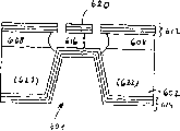
图6a示出了根据本发明的一种特定标准具结构600的剖面图。可以在平板或衬底602中制造标准具600,例如在微电子工业中典型常规采用的硅晶片。可以在衬底602的一个侧面中形成具有倾斜侧壁605的凹槽604。这种特定结构是通过湿法各向异性蚀刻在<100>硅中制造的典型谐振腔,这里蚀刻停止在蚀刻停止层例如氧化硅或重掺杂的硅上。可以采用另一种蚀刻方法,例如深反应离子腐蚀。其中形成凹槽604的衬底602的侧面将称为标准具的“背面”606。在与凹槽604相对的衬底602的一侧上形成由不同于衬底602的材料制造的间隔层608。间隔层608的外表面将称为标准具600的“前表面”607。电介质涂层的多层薄膜叠层612、614分别覆盖标准具的前表面和背面607、606。在衬底602的平坦前表面上形成的前侧面涂层612非常平坦。背面涂层614为保形并均匀覆盖凹槽侧壁605、基底603和背面606。可以在凹槽604之上位置中心的两个电介质叠层612、614之间设置空气隙616。可以通过在顶部电介质叠层612中形成的蚀刻孔蚀刻间隔层608来产生空气隙616。多层电介质涂层612、614根据各层的数量、各层的次序、各层的折射系数和各层的厚度来构成,以便起电介质反射器的作用,例如作为本领域公知的薄膜光学元件并作为在光学元件上常规采用制造的反射和抗反射涂层。例如,涂层612、614可以由二氧化硅(大约1.46的折射系数)和氮化硅(大约2.0的折射系数)的交替层组成。干涉滤光片的元件层的光学厚度(即,实际物理厚度乘以所关心波长下的材料层的折射系数)可以制造为对应于激光器发光波长的四分之一波长或其倍数。可以在同一工艺中淀积前电介质涂层和背面电介质涂层612、614,以致前侧面涂层和背面涂层612、614具有非常相近的相同光学特性和传输特性。淀积电介质层的适合方法包括热蒸发、电子束蒸发、溅射淀积和化学气相淀积。化学气相淀积(CVD)包括低压CVD和等离子体增强CVD,因为它们是保形的并用于同时淀积前涂层和背面涂层612、614,所以原子层淀积是吸引光子。应当看出,图6a的微加工标准具120的结构展示了图2中所示的标准具的基本特征,就是说通过空气隙或透明材料的薄片分离两个干涉滤光片。Figure 6a shows a cross-sectional view of a specific etalon structure 600 according to the present invention. The etalon 600 may be fabricated in a flat plate or
现在,回到标准具600的制造,本发明还提供一种制造标准具600的方法,图6b-6h中说明了步骤的顺序。图6a-6f和图6h是剖面图,以及图6g是顶视图。应当理解,在此描述的技术说明了步骤的一种顺序,步骤顺序可以按需要采用建立并使用常规微加工技术,但是本领域普通技术人员应当清楚,这些步骤的各种变化和对这些步骤的各种替换也可以制造具有实质上相同特性和功能的结构。Now, returning to the manufacture of the etalon 600, the present invention also provides a method of manufacturing the etalon 600, the sequence of steps is illustrated in Figures 6b-6h. Figures 6a-6f and Figure 6h are cross-sectional views, and Figure 6g is a top view. It should be understood that the techniques described herein illustrate a sequence of steps that can be adapted as desired to establish and use conventional microfabrication techniques, but that various changes to and modifications to these steps will be apparent to those of ordinary skill in the art. Various substitutions may also produce structures having substantially the same properties and functions.
在图6b中,在衬底602例如硅晶片上淀积或以其它方式形成间隔材料层608。由于它的表面光滑且平坦、并且可控制蚀刻的特性,在两个侧面上已抛光的单晶硅晶片是衬底602的较好选择。其它适宜的衬底包括玻璃、陶瓷、熔合二氧化硅、石英或其它类型的半导体晶片。典型地,硅衬底602具有大约0.5毫米的厚度,并且间隔层608具有2微米至30微米的厚度范围。可选择地,衬底602可以是绝缘体硅(SOI)结构,该绝缘体硅(SOI)结构具有将∽0.5mm厚的硅晶片与淀积2-30微米厚的硅层进行分离的0.1-2微米厚的埋置的二氧化硅层。应当注意,衬底不必对激光器波长是透明的,因为凹槽604的形成就从激光束的光学路径中去除了所有衬底材料。材料选择的基本原理是衬底材料相对于间隔层材料可以被选择性蚀刻。许多材料的组合满足这种需求,许多材料的组合包括在作为衬底602的未掺杂或轻掺杂的硅衬底上淀积的掺硼或掺杂其它杂质的硅间隔层608、或在蓝宝石衬底602上淀积硅间隔层608。在前一种情况下,掺杂间隔层608使其可抵抗否则会用蚀刻的未掺杂或轻掺杂的硅的蚀刻。In FIG. 6b, a
在一个期望的实施例中,衬底602可以是单晶硅晶片,并且间隔材料608是重掺杂硼的硅。可以通过掺杂硼层的外延生长或离子注入进入硅晶片602来形成掺杂硼的硅层608。In one desired embodiment,
如图6c中所示,可以按照穿过衬底602形成锥形孔的形式来蚀刻出穿过衬底602的凹槽604,衬底602具有间隔层608,用间隔层608作为停止蚀刻阻挡层(或氧化物提供蚀刻停止,该氧化物与SOI硅晶片情况下的间隔层接触)。在硅衬底602例如(100)硅的情况下,可以采用氢氧化钾(KOH)溶液作为各向异性蚀刻剂,以提供凹槽604的侧壁锥形。可以用于此目的的其它蚀刻剂包括联氨和EDP(乙二胺焦邻苯二酚)。而且,当处于典型具有其它衬底材料例如陶瓷的情况时,还可以采用各向同性蚀刻剂。所需蚀刻剂的特性是它比间隔层材料更快地去除衬底材料。可选择地,在SOI晶片的情况下,需要蚀刻剂相对于埋置氧化层的选择性。间隔层608处的凹槽604的典型直径为100-500微米,尽管该尺寸可以完全根据应用和光谐振腔103中的发射激光的元件102的光束细窄部分尺寸而改变。As shown in FIG. 6c, a
如图6d中所示,在衬底的前表面607上形成多层薄膜电介质叠层612,该电介质叠层612形成光学干涉滤光片,并且在衬底的背面606上形成电介质叠层614。根据在薄膜光学中广泛采用的方法来设计并淀积具有交错的高折射系数和低折射系数以及四分之一波长厚度的多层结构。各层可以由例如二氧化硅、氮化硅或包括金属氧化物和宽禁带宽度的半导体如氮化镓或碳化硅的其它电介质材料组成。根据层的数量和设计的中心波长,前侧电介质叠层或背面电介质叠层的典型总厚度可以是2-15微米。As shown in Figure 6d, a multilayer thin film
如图6e中所示,在前电介质叠层612中可以形成一组通孔618。通孔暴露下面的间隔层608,使间隔层608易于进行蚀刻。可以通过结合湿法或干法蚀刻(例如,反应离子蚀刻)的光刻或通过例如激光钻孔的其它方法来限定通孔618。通孔618可以位于凹槽604之上,或在凹槽604的四周并在衬底602之上。典型的通孔直径可以是10-50微米。如图6f中所示,通过性刻去除直接位于凹槽604之上的间隔层608的部分,在前侧电介质叠层612和背面电介质叠层614之间保留空气隙616,并且其中空气隙616与凹槽604对准。As shown in FIG. 6e , a set of
间隔层608的所述蚀刻易于使用用于衬底602和间隔层608的几种材料组合、并且易于使用大分子式表示的蚀刻剂。例如,如果间隔层608是未掺杂的硅或是掺硼的硅并且衬底602是硅,那么就可以用二氟化氙蚀刻间隔层608。当衬底602用电介质层例如氮化物和氧化物覆盖时,二氟化氙气体容易各向同性蚀刻硅,但保留衬底602不受损伤。还可以采用液体蚀刻剂。虽然衬底602的一些轻微蚀刻可以忍受,但是蚀刻剂应该不显著蚀刻电介质叠层612、614或使电介质叠层612、614变得粗糙。由于蚀刻间隔层608的一部分,就在空气隙616之上悬置前侧电介质叠层612的一部分。The etching of the
图6g中示出了用于蚀刻间隔层608的示例性的通孔图形的顶视图,作为围绕正方形图形排列的8个通孔618的情况。图6f的虚线矩形示出了面积的大致范围,此处从间隔层608中通过蚀刻挖凿出的缝隙616将两个平行的电介质叠层反射器612、614分离。在图6g中,虚线矩形还大致对应于部分前侧薄膜电介质叠层612的顶视图,该电介质叠层612的部分悬置在空气隙616之上并由图6f中的620表示。该区域作为标准具600的光学功能部分、提供激光束的光学干涉效果。环绕凹槽604的未蚀刻衬底部分(即,在图6g的顶视图中的矩形虚线区域之外的区域,或对应于图6f的剖面图中的(622)表示的衬底部分)给予标准具600的机械稳定性,并且还使用于在光谐振腔103中操作方便并安装标准具600。衬底602还支撑安装并对准参考表面以便易于标准具600的精确定位和取向。由于微加工标准具600的几何设计,环绕凹槽604的部分622表示的相对于衬底602的体部分不对标准具600的光学路径长度起作用。在这种设计中,涂层需要的净应力应当用典型的所需的小的净张应力来控制。A top view of an exemplary via pattern for
标准具600可以设置有附加结构以便允许它的调谐。在图6h的剖面图中表示了静电激励的标准具600,在前电介质叠层区域620的外侧上形成导电电极624,其悬置在空气隙616之上。该电极组是公共电极,即电连接的。如果衬底602足以导电,那么它就可以作为相反电极。可选择地,以第二导电焊盘例如由氧化铟锡(ITO)组成的形式,在作为相反电极626的背面电介质叠层614的外表面上淀积相反电极626。氧化锡和ITO具有在于光纤通讯所应用的波长下为透明的优点,由此避免了光学路径的模糊。在电极624和相反电极626(或多个相反电极)之间施加的电压提供拉伸或抵制悬置的电介质叠层620的静电力,由此改变电介质叠层614和620之间的空气隙616的间隔。这就改变了标准具600的传输特性,特别地,使窄传输频带(图3中302所示)的波长漂移。因此,这种标准具结构提供传输频带的调谐,结果,由此通过施加的电信号来提供波长调谐。The etalon 600 may be provided with additional structures to allow its tuning. Electrostatically actuated etalon 600 is shown in cross-section in FIG. 6h , with conductive electrodes 624 formed on the outside of front
图7d中示出了用于外谐振腔激光器100中的微加工标准具120的标准具700的可替换实施例,图7a-7d示出了它的制造步骤的示例性顺序。图7a示出了在其一个侧面703上形成电介质叠层704的衬底702。电介质叠层704可以是结构上、组分上、功能上类似于关于图6中描述的电介质叠层612、614。图7b示出了分离衬底706,在分离衬底706中通过掩模并控制蚀刻或钻孔、在衬底的一个侧面中形成浅凹陷708,并且衬底的相同侧面705已经保形地覆盖有电介质叠层710。如图7c中所示,对准并安装两个衬底702、706或将两个衬底702、706键合在一起,以致凹陷708提供在两个侧面上由电介质叠层704和710键合的内部空间或空气隙712。如图7c中所示,此结构提供具有空气隙空间d的标准具700。如图7d中所示,去除两个衬底702、706的部分,以形成对准的凹槽714和716,其展示了两个粘接空气隙712的无支撑电介质叠层718和720。如关于图6g中的解释,以导电焊盘或导电氧化物膜形式的电极可以应用于无支撑电介质叠层,该无支撑电介质叠层用于静电激励并且电控制标准具缝隙712的调谐。An alternative embodiment of an
实施例Example
本发明的显著特征是微加工标准具的紧凑并与相应缩短的光谐振腔103的光学路径长度易于更加优化模式间隔和模式选择的更简单方法。在以下模型和模拟实施例中进一步示例出本发明的这些方面。A notable feature of the present invention is the compactness of the micromachined etalon and the correspondingly shortened optical path length of the optical cavity 103 allows for a simpler method of more optimized mode spacing and mode selection. These aspects of the invention are further exemplified in the following modeled and simulated examples.
图8a示出了在1550nm波长中心的光谱范围内、用于24mm的有效总光谐据腔长度lcav,eff的纵向波长模式的计算梳形。模式间隔为大约0.5nm。图8b示出了类似模拟将激光器谐振腔的总光学路径长度缩短至12mm的结果。可以预料,模式间隔从第一实施例的模式间隔增加到大约1nm。图8a和8b说明了光谐振腔长度对模式间隔的作用,并且较短的光谐振腔导致更宽的间隔模式,对于波长识别、模式选择器件就需要较少的苛刻的解决需求。Figure 8a shows the calculated comb shape of the longitudinal wavelength mode for an effective total optical resonance cavity length l cav,eff of 24 mm in the spectral range centered at 1550 nm wavelength. The mode spacing is about 0.5 nm. Figure 8b shows the results of similar simulations shortening the total optical path length of the laser resonator to 12 mm. It is expected that the mode spacing increases to about 1 nm from that of the first embodiment. Figures 8a and 8b illustrate the effect of the length of the optical resonator on the mode spacing, and a shorter optical resonator leads to a wider spaced mode, which requires less stringent solution requirements for wavelength discrimination and mode selection devices.
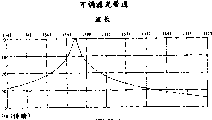
图8c(粗略说明)和图8d(更细说明)示出了标准具的计算光谱传输,标准具由5.8微米的空气隙分离的两个电介质叠层组成,电介质叠层为氮化硅和二氧化硅的20层交替层,每层为四分之一波长厚度(=λ/4n,这里λ=1550nm,n是适用于二氧化硅或氮化硅的折射系数)。传输通带的FWHM为大约0.3nm。该标准具的FSR(自由光谱范围)、即相邻传输通带峰值之间的波长间隔为大约90nm。该FSR明显大于典型1550-nm波长发射激光器的增益带宽,为了防止维持超过一种激光模式,图4和图5中的相关讨论中规定了这种要求。此外,示例性的微加工标准具的分辨率适合于解决12-mm长光谐振腔情况下的相邻峰值。如图8d中所见,在峰值传输的1nm之内的模式,存在大约15dB衰减。所有这些实施例是单带通计算,而且双通实质上增加了带通之间的衰减。给定应用下所需的衰减将依赖各种变量,包括待使用的激光元件的增益曲线。获得的抑制易于通过增加或减少电介质反射器的数量来进行调整。Figure 8c (rough illustration) and Figure 8d (more detailed illustration) show the calculated spectral transmission of an etalon consisting of two dielectric stacks separated by a 5.8 μm air gap, the dielectric stack being silicon nitride and
参照缝隙调节的上述标准具的电势调谐能力表示为图8e中所示的三个光谱传输曲线。以8nm的增量,缩短5.8微米的空气隙,产生了传输峰值的可评估的漂移,以分别缩短至如曲线802、804和806所示的波长。曲线802是用于具有5.820微米缝隙的标准具。曲线804是用于通过8nm缩短至5.812微米的缝隙,并且曲线806是用于进一步缩短至5.804微米的缝隙。因此,模拟示出了空气隙的相对适度的修正,因而易于通过静电激励效果来获得,对于1微米的模式间隔产生有用的波长识别,该模式间隔出现在具有12mm的有效光学长度的光谐振腔103中。通过1-35度的角度来倾斜微加工标准具120将获得传输特性的类似修正。The potential tuning capability of the above etalon adjusted with reference to the slit is represented by the three spectral transmission curves shown in Fig. 8e. Shortening the 5.8 micron air gap in 8 nm increments produces an appreciable shift in the transmission peak to shorten to wavelengths as shown by curves 802, 804, and 806, respectively. Curve 802 is for an etalon with a 5.820 micron gap. Curve 804 is for a gap shortened by 8 nm to 5.812 microns, and curve 806 is for a gap shortened further to 5.804 microns. Thus, the simulations show that a relatively modest modification of the air gap, and thus easily obtained by electrostatic excitation effects, yields useful wavelength discrimination for a mode separation of 1 micrometer, which occurs in an optical resonant cavity with an effective optical length of 12 mm 103 in. Tilting the micromachined etalon 120 by an angle of 1-35 degrees will obtain a similar correction of the transmission characteristics.
在本发明的一个具体实施例中,对光学路径长度的重要影响是:In a specific embodiment of the invention, the significant influence on the optical path length is:
i、具有物理长度dlas=250微米和大约850微米的光学长度的边缘发射激光器102。i. An edge emitting laser 102 with a physical length dlas = 250 microns and an optical length of about 850 microns.
ii、400微米直径的,由Spinel制造并具有大约720微米的光学路径长度的抗反射涂覆的球面透镜116。ii. 400 micron diameter anti-reflection coated spherical lens 116 manufactured by Spinel and having an optical path length of approximately 720 microns.
iii、例如,由10-20层的氮化硅和二氧化硅组成的可调谐标准具120,由形成如图6g中所示标准具120中的晶片的外围区域之外形成的框架支撑。结果,标准具光学路径长度为大约500微米,并且应当注意,该厚度基于允许插入其中形成标准具120的硅晶片的空间。当激光束路径限制于在硅衬底中形成的凹槽时,光学路径不通过穿过硅的传输而增加。iii. For example, a tunable etalon 120 composed of 10-20 layers of silicon nitride and silicon dioxide, supported by a frame formed outside the peripheral area of the wafer forming the etalon 120 as shown in FIG. 6g. As a result, the etalon optical path length is approximately 500 microns, and it should be noted that this thickness is based on the space allowed for insertion of the silicon wafer into which etalon 120 is formed. When the laser beam path is limited to grooves formed in the silicon substrate, the optical path is not augmented by transmission through the silicon.
总体上,这些三个元件(发射激光的元件102、标准具120和透镜116)之间的空间可制造成小于1毫米。Overall, the space between these three elements (laser emitting element 102, etalon 120, and lens 116) can be fabricated to be less than 1 mm.
假设这些光学路径如下:850微米(激光器)+720微米(透镜)+515微米(标准具)+1毫米(缝隙空间)=~3毫米,给出了大约3毫米的最小总光学路径长度。因此,根据所需的梳状间隔,就可以将元件设置为具有更加宽松或开放的间隔。Assuming these optical paths are as follows: 850 microns (laser) + 720 microns (lens) + 515 microns (etalon) + 1 mm (gap space) = ~3 mm, giving a minimum total optical path length of about 3 mm. Thus, depending on the desired comb spacing, elements can be arranged with more loose or open spacing.
本发明还提供通过用光检测器监测激光器输出,使用微加工可调谐标准具简单并精确控制激光器反射波长,图9a中示意性地示出了其一个示例性实施例。图9a中所示的系统包含激光器902、校直透镜904,以及透镜906和限定其间的光谐振腔910的高反射涂覆小面908。通过涂覆的小面908传输激光束输出912。系统还包含在输出光束912上设置的光束分离器914,用于接收输出光束912的分离部分的光检测器916,脉冲计数器电路918、控制器920和用于激励微加工标准具924的电路922。如此设置的光检测器916连续监测激光器输出。当激光器切换或在模式之间跳变时,在它的光输出中存在短暂的中断,其光输出可以被检测并寄存为脉冲。当控制器920清除整个光谱范围的电激励标准具时,计数器电路918就感应出模式跳变的发生并计数模式跃迁的数量,其包含了具有固定波长反射模式的系统的反射波长。然后,检测器916提供反馈,以便优化标准具924的定位,以便在所需操作模式下优化功率。在装配工艺期间或通过TEC上的温度调节系统调节至一个温度,就可以设置梳状模式的绝对位置,在所述的一个温度下纵向模式的模式梳状处于中心。The present invention also provides simple and precise control of the laser reflected wavelength using a micromachined tunable etalon by monitoring the laser output with a photodetector, an exemplary embodiment of which is schematically shown in Figure 9a. The system shown in Figure 9a comprises a
在图9a描述的系统中,一些误操作、噪声影响或其它故障可能引起模式跳变会丢失模式的轨迹,导致模式偏移误差。可选择地,制造可变总光学路径长度可以产生起始模式的变化。通过建立本地信道波长就能够进行补救,如图9b中所示,系统使用该本地信道波长,以便建立固定基准点。除了第二光束分离器926、对“本地”信道进行调谐的滤光片928和第二光检测器930之外,图9b的系统类似于图9a的系统。衍射光栅、棱镜、标准具或类似器件可以用作代替滤光片928。第二光束分离器926连续对激光器输出进行取样,通过低通光学干涉滤光片928来过滤激光器输出,其只将基准波长的激光器输出传输到第二光检测器930。由第二光检测器930寄存的信号表示在对应于基准波长的模式下工作的激光器902。因此,控制器920通过跳变电压激励标准具924来清除整个模式,并且通过光检测器916和计数电路918来统计清除中的转换的模式数量。因此,可以将激光器902调谐为所需的任何模式,并能够从基准模式中统计模式跳变的数量。In the system depicted in Fig. 9a, some misoperations, noise effects or other failures may cause mode hopping and lose the track of the mode, resulting in mode shift error. Alternatively, fabricating a variable total optical path length can produce variations in the starting mode. Remedy can be achieved by establishing a local channel wavelength, which is used by the system, as shown in Figure 9b, in order to establish a fixed reference point. The system of FIG. 9b is similar to the system of FIG. 9a except for the second beam splitter 926, the filter 928 for tuning the "local" channel, and the second photodetector 930. Diffraction gratings, prisms, etalons, or similar devices may be used in place of filter 928 . The second beam splitter 926 continuously samples the laser output and filters the laser output through a low-pass optical interference filter 928 , which transmits only the laser output at the reference wavelength to the second photodetector 930 . The signal registered by the second photodetector 930 indicates that the
从上述说明书中,本发明的这些和其它优点对于本领域普通技术人员将是明显的。因此,本领域普通技术人员应当认识到,在不脱离本发明的宽发明观念内,可以对上述实施例进行变化和修改。因此,应当理解,本发明不限于在此描述的具体实施例,但是本发明希望包含权利要求书提出的本发明的范围和精神之内的所有变化和修改。These and other advantages of the invention will be apparent to those of ordinary skill in the art from the foregoing description. Accordingly, those of ordinary skill in the art will recognize that changes and modifications can be made to the above-described embodiments without departing from the broad inventive concept of the invention. It is therefore to be understood that this invention is not limited to the particular embodiments described herein, but it is intended to cover all changes and modifications within the scope and spirit of the invention as set forth in the appended claims.
Claims (11)
Priority Applications (1)
| Application Number | Priority Date | Filing Date | Title |
|---|---|---|---|
| CNA2004100903103A CN1700540A (en) | 2004-05-21 | 2004-05-21 | External resonator semiconductor laser and manufacturing method thereof |
Applications Claiming Priority (1)
| Application Number | Priority Date | Filing Date | Title |
|---|---|---|---|
| CNA2004100903103A CN1700540A (en) | 2004-05-21 | 2004-05-21 | External resonator semiconductor laser and manufacturing method thereof |
Related Child Applications (1)
| Application Number | Title | Priority Date | Filing Date |
|---|---|---|---|
| CNA200710300512XA Division CN101295855A (en) | 2004-05-21 | 2004-05-21 | External resonator semiconductor laser and manufacturing method thereof |
Publications (1)
| Publication Number | Publication Date |
|---|---|
| CN1700540A true CN1700540A (en) | 2005-11-23 |
Family
ID=35476459
Family Applications (1)
| Application Number | Title | Priority Date | Filing Date |
|---|---|---|---|
| CNA2004100903103A Pending CN1700540A (en) | 2004-05-21 | 2004-05-21 | External resonator semiconductor laser and manufacturing method thereof |
Country Status (1)
| Country | Link |
|---|---|
| CN (1) | CN1700540A (en) |
Cited By (2)
| Publication number | Priority date | Publication date | Assignee | Title |
|---|---|---|---|---|
| JP2020109856A (en) * | 2014-06-05 | 2020-07-16 | レニショウ パブリック リミテッド カンパニーRenishaw Public Limited Company | Laser device |
| CN113937616A (en) * | 2021-09-26 | 2022-01-14 | 中国科学院长春光学精密机械与物理研究所 | Semiconductor laser array, semiconductor laser single tube and preparation method thereof |
-
2004
- 2004-05-21 CN CNA2004100903103A patent/CN1700540A/en active Pending
Cited By (3)
| Publication number | Priority date | Publication date | Assignee | Title |
|---|---|---|---|---|
| JP2020109856A (en) * | 2014-06-05 | 2020-07-16 | レニショウ パブリック リミテッド カンパニーRenishaw Public Limited Company | Laser device |
| JP7199393B2 (en) | 2014-06-05 | 2023-01-05 | レニショウ パブリック リミテッド カンパニー | laser device |
| CN113937616A (en) * | 2021-09-26 | 2022-01-14 | 中国科学院长春光学精密机械与物理研究所 | Semiconductor laser array, semiconductor laser single tube and preparation method thereof |
Similar Documents
| Publication | Publication Date | Title |
|---|---|---|
| JP4916647B2 (en) | External cavity semiconductor laser and manufacturing method thereof | |
| US8831049B2 (en) | Tunable optical system with hybrid integrated laser | |
| CN100350685C (en) | Error Signal Generation System | |
| US6483635B1 (en) | Apparatus for light amplification | |
| EP1363370B1 (en) | Fixed wavelength vertical cavity optical devices and method of manufacture thereof | |
| KR20200124284A (en) | External cavity quantum cascade laser | |
| KR101459495B1 (en) | Tunable laser device | |
| CN1275056C (en) | MEMS reconfigurable optical grating | |
| US20040013431A1 (en) | Laser and laser signal combiner | |
| US7221828B2 (en) | Optical wave length division multiplexing module and communication system using the same | |
| CN1930748A (en) | Semi-integrated designs for external cavity tunable lasers | |
| JP2002500386A (en) | Integrated optical transceiver | |
| CN1531768A (en) | External cavity laser with selective thermal control | |
| KR102237784B1 (en) | Laser Device with wavelength stabilizer | |
| CN1177421A (en) | Laser device | |
| KR101519628B1 (en) | Compact Tunable Laser Device | |
| US20030133485A1 (en) | Laser array for generating stable multi-wavelength laser outputs | |
| US20180348507A1 (en) | Wavelength tunable optical sources, filters and detectors | |
| JP2002299755A (en) | Fast and broadband tunable laser | |
| TWI227799B (en) | Resonant reflector for increased wavelength and polarization control | |
| CN1700540A (en) | External resonator semiconductor laser and manufacturing method thereof | |
| CN101295855A (en) | External resonator semiconductor laser and manufacturing method thereof | |
| EP1811619A2 (en) | External cavity semiconductor laser and method for fabrication thereof | |
| US9577402B2 (en) | Variable-wavelength light source | |
| US6768841B2 (en) | Integrated optical interleaver/de-interleaver |
Legal Events
| Date | Code | Title | Description |
|---|---|---|---|
| C06 | Publication | ||
| PB01 | Publication | ||
| C10 | Entry into substantive examination | ||
| SE01 | Entry into force of request for substantive examination | ||
| C12 | Rejection of a patent application after its publication | ||
| RJ01 | Rejection of invention patent application after publication |
Open date: 20051123 |