CN1723552A - Reduced splattering of unpassivated laser fuses - Google Patents
Reduced splattering of unpassivated laser fuses Download PDFInfo
- Publication number
- CN1723552A CN1723552A CNA038222558A CN03822255A CN1723552A CN 1723552 A CN1723552 A CN 1723552A CN A038222558 A CNA038222558 A CN A038222558A CN 03822255 A CN03822255 A CN 03822255A CN 1723552 A CN1723552 A CN 1723552A
- Authority
- CN
- China
- Prior art keywords
- barrier
- explosion
- fuse
- laser
- fusible
- Prior art date
- Legal status (The legal status is an assumption and is not a legal conclusion. Google has not performed a legal analysis and makes no representation as to the accuracy of the status listed.)
- Granted
Links
Images




Classifications
-
- H—ELECTRICITY
- H10—SEMICONDUCTOR DEVICES; ELECTRIC SOLID-STATE DEVICES NOT OTHERWISE PROVIDED FOR
- H10D—INORGANIC ELECTRIC SEMICONDUCTOR DEVICES
- H10D89/00—Aspects of integrated devices not covered by groups H10D84/00 - H10D88/00
-
- H—ELECTRICITY
- H10—SEMICONDUCTOR DEVICES; ELECTRIC SOLID-STATE DEVICES NOT OTHERWISE PROVIDED FOR
- H10W—GENERIC PACKAGES, INTERCONNECTIONS, CONNECTORS OR OTHER CONSTRUCTIONAL DETAILS OF DEVICES COVERED BY CLASS H10
- H10W20/00—Interconnections in chips, wafers or substrates
- H10W20/40—Interconnections external to wafers or substrates, e.g. back-end-of-line [BEOL] metallisations or vias connecting to gate electrodes
- H10W20/49—Adaptable interconnections, e.g. fuses or antifuses
- H10W20/493—Fuses, i.e. interconnections changeable from conductive to non-conductive
- H10W20/494—Fuses, i.e. interconnections changeable from conductive to non-conductive changeable by the use of an external beam, e.g. laser beam or ion beam
Landscapes
- Design And Manufacture Of Integrated Circuits (AREA)
- Fuses (AREA)
- Internal Circuitry In Semiconductor Integrated Circuit Devices (AREA)
Abstract
Description
技术领域technical field
本发明总体上涉及集成电路的制造,尤其是防止在非钝化激光熔丝烧断时熔丝材料的飞溅在其它的激光熔丝中产生短路。The present invention relates generally to the fabrication of integrated circuits, and more particularly to preventing spattering of fuse material from creating short circuits in other laser fuses when non-passivated laser fuses are blown.
背景技术Background technique
在集成电路的制造中,已经有很长时间在使用激光熔丝。激光熔丝的一种应用是根据集成电路的预定用途,激活或者停用集成电路中的特定功能。例如,可以对集成电路进行单一设计,使之具有完备的功能集合。但是,取决于集成电路销售时的价格,可以禁用特定的功能。在另一种应用中,激光熔丝允许用正常工作的备用器件和电路来替换集成电路中有缺陷的器件和电路。一般,当对集成电路进行测试以验证其工作性能时,测试设备对集成电路的有缺陷的部分进行标记(或者存储起来)。随后,进行一个单独的操作,将特定的激光熔丝烧断,以去除有缺陷的器件和电路,用能够工作的器件和电路替换之。In the manufacture of integrated circuits, laser fuses have been used for a long time. One application of laser fuses is to activate or deactivate specific functions in an integrated circuit, depending on the intended use of the integrated circuit. For example, an integrated circuit can be single designed to have a complete set of functions. However, depending on the price at which the integrated circuit is sold, certain functions may be disabled. In another application, laser fuses allow defective devices and circuits in integrated circuits to be replaced with functioning spares and circuits. Typically, when an integrated circuit is tested to verify its operational performance, the test equipment flags (or stores) the defective portions of the integrated circuit. Then, in a separate operation, specific laser fuses are blown to remove defective devices and circuits and replace them with working devices and circuits.
顾名思义,使用有效熔化并且随后蒸发可熔断的连接的高能量激光来烧断激光熔丝。在可熔断连接熔断时,蒸发的熔丝材料有可能不受控制地飞溅到相邻的熔丝。飞溅的熔丝材料进而可能导致相邻熔丝工作不正确,也就是导致先前被熔断的熔丝表现得像未熔断的熔丝一样,或者使相邻的已熔断的熔丝一起短路。如果发生这种情况,则集成电路不能正常地工作。As the name implies, laser fuses are blown using a high-energy laser that effectively melts and then vaporizes the fusible link. When the fusible link is blown, there is the potential for uncontrolled splashing of evaporated fuse material onto adjacent fuses. Splashed fuse material may in turn cause adjacent fuses to operate incorrectly, ie, cause a previously blown fuse to behave like an unblown fuse, or cause adjacent blown fuses to short together. If this happens, the integrated circuit cannot function properly.
激光熔丝有两种主要形式,钝化的非钝化的。钝化激光熔丝在顶部有一个钝化层,以保护激光熔丝不受工作环境的损害。对于用易腐蚀的材料比如铜(Cu)制成的可熔断连接来说,钝化层的使用尤其重要。非钝化激光熔丝不具有钝化层,容易受到不友好的环境的损害。由于非钝化激光熔丝对环境是开放的,倾向于用抗腐蚀(或者相对来说抗腐蚀的)材料比如铝(Al)制造非钝化激光熔丝。钝化激光熔丝对蒸发熔丝材料的飞溅非常不敏感,这是由于钝化层提供了保护。另一方面,钝化层使得激光熔丝更难以熔断。这是由于用来熔断熔丝的激光必须具有足够的能量来在能够蒸发熔丝材料之前穿透钝化层,建立足够大的压强来使可熔断连接顶部的钝化层破裂而释放出蒸发材料。Laser fuses come in two main forms, passivated and non-passivated. Passivated laser fuses have a passivation layer on top to protect the laser fuse from the operating environment. The use of a passivation layer is especially important for fusible links made of corrodible materials such as copper (Cu). Non-passivated laser fuses do not have a passivation layer and are vulnerable to damage from hostile environments. Since non-passivated laser fuses are open to the environment, there is a tendency to fabricate non-passivated laser fuses from corrosion-resistant (or relatively corrosion-resistant) materials such as aluminum (Al). Passivated laser fuses are very insensitive to splashing of evaporating fuse material due to the protection provided by the passivation layer. On the other hand, the passivation layer makes it more difficult for the laser fuse to blow. This is due to the fact that the laser used to blow the fuse must have enough energy to penetrate the passivation layer before being able to vaporize the fuse material, building up enough pressure to rupture the passivation layer on top of the fusible link and release the evaporated material .
另一方面,钝化使得能够安全地熔断激光熔丝,不会影响相邻的电路。这是因为,钝化层防止了可熔断连接的熔化材料立即、猛烈的释放。有时,在熔丝熔断过程中,在可熔断连接被激光最初熔化之后,可熔断连接吸收了足够多的能量,使得被加热的可熔断连接被蒸发。蒸发的材料产生一个压强,该压强势必使其包裹材料在材料的最脆弱点破裂。最脆弱点一般是覆盖的钝化层。从所述破裂爆出的蒸发材料本身当重新淀积到芯片表面上时,淀积为非常薄的不导电膜。Passivation, on the other hand, enables safe blowing of laser fuses without affecting adjacent circuits. This is because the passivation layer prevents the immediate, violent release of the molten material of the fusible connection. Sometimes, during fuse blowing, after the fusible link is initially melted by the laser, enough energy is absorbed by the fusible link that the heated fusible link is vaporized. The evaporated material creates a pressure that tends to rupture its enveloping material at the most vulnerable point of the material. The most vulnerable point is generally the overlying passivation layer. Evaporated material bursting from the rupture itself deposits as a very thin non-conductive film when redeposited onto the chip surface.
在使用机械稳定性低,比如低k电介质的材料制造的集成电路中,蒸发熔丝材料的释放导致的破裂可能不仅出现在钝化层中,而且可以出现在下伏的电介质层中。这会对电路造成严重的损伤,尤其是如果把对腐蚀敏感的材料比如铜用于金属导线的话。在这种情况下,在这样的集成电路上设置非钝化熔丝,以减少在熔丝熔断过程中下伏表面受损的机会。为了对下伏表面提供额外的保护措施,可以在熔丝层(fuse level)和下伏表面之间设置一个硬电介质层。不幸的是,如果没有钝化层,熔丝熔断过程会受到以下方面的影响:熔化的熔丝材料可能在没有足够热量的时候蒸发,这阻止了熔化的金属全部蒸发。熔化金属的部分蒸发可能导致仍然保持为液体形式的熔丝材料的飞溅。飞溅的熔丝材料可能导致与正在熔断的熔丝相邻的非钝化熔丝的电短路。飞溅效应取决于许多参数,比如激光的功率和波长,可熔断连接的尺寸,熔丝的材料等。In integrated circuits fabricated using materials with low mechanical stability, such as low-k dielectrics, cracking due to release of evaporated fuse material may occur not only in the passivation layer, but also in the underlying dielectric layer. This can cause serious damage to the circuit, especially if corrosion-sensitive materials such as copper are used for the metal wires. In such cases, non-passivated fuses are provided on such integrated circuits to reduce the chance of damage to the underlying surface during blowing of the fuse. To provide an additional measure of protection to the underlying surface, a hard dielectric layer can be placed between the fuse level and the underlying surface. Unfortunately, without a passivation layer, the fuse blowing process suffers from the fact that the molten fuse material may evaporate without sufficient heat, which prevents the molten metal from fully evaporating. Partial evaporation of the molten metal may result in splashing of the fuse material which remains in liquid form. Splashed fuse material may cause an electrical short to a non-passivated fuse adjacent to the blowing fuse. The spatter effect depends on many parameters, such as the power and wavelength of the laser, the size of the fusible link, the material of the fuse, etc.
美国专利6,160,302提出了在激光熔丝之间形成壁,以防止未对准的激光意外熔断与激光要熔断的熔丝相邻的熔丝。US Patent 6,160,302 proposes forming walls between laser fuses to prevent a misaligned laser from accidentally blowing a fuse adjacent to the fuse the laser is trying to blow.
美国专利6,300,232提出了围绕单个的激光熔丝建立阻挡,以防止在熔丝熔断步骤中激光产生的热导致的物理损伤的扩展。US Patent 6,300,232 proposes creating a barrier around individual laser fuses to prevent propagation of physical damage caused by laser generated heat during the fuse blowing step.
美国专利5,899,736提出用电介质阻挡部分来围住个体的电可熔断连接,以防止喷射的熔丝材料的选出。US Patent No. 5,899,736 proposes surrounding individual electrically fusible links with dielectric barriers to prevent escape of ejected fuse material.
因此,需要有一种方法,对正在被熔断的激光熔丝邻近的激光熔丝提供保护,但是在额外的空间需求和/或额外的制造步骤方面不会显著增加成本。Accordingly, there is a need for a method of providing protection to laser fuses adjacent to the laser fuse being blown without significantly increasing cost in terms of additional space requirements and/or additional manufacturing steps.
发明内容Contents of the invention
在一个方面,本发明提供了一种半导体器件,其包括第一电接点焊盘、第二电接点焊盘以及由导电材料制成的可熔断连接,该可熔断连接具有连接到第一电接点焊盘的第一端部和连接到第二电接点焊盘的第二端部,该可熔断连接要在施加一个能量源之后变为不导电的,水平地包围所述可熔断连接的一个爆炸阻挡体,用以容纳由于施加所述能量源而射出的可熔断连接材料。In one aspect, the present invention provides a semiconductor device comprising a first electrical contact pad, a second electrical contact pad, and a fusible link made of a conductive material, the fusible link having a connection to the first electrical contact pad. The first end of the pad and the second end connected to the second electrical contact pad, the fusible connection is to become non-conductive after application of a source of energy, horizontally surrounding an explosion of the fusible connection The blocking body is used for containing the fusible connection material ejected due to the application of the energy source.
在另一方面,本发明提供了一种对半导体器件建立爆炸阻挡体的方法,包括下述步骤:形成第一和第二电接点焊盘,形成连接到第一和第二电接点焊盘的可熔断连接,以及形成导电爆炸阻挡体,该爆炸阻挡体具有平行于所述可熔断连接形成的第一部件,以及平行于所述可熔断连接形成的、在可熔断连接的与所述第一部件相反的一侧的第二部件。In another aspect, the present invention provides a method of creating an explosion barrier to a semiconductor device, comprising the steps of: forming first and second electrical contact pads, forming a connection to the first and second electrical contact pads a fusible connection, and forming an electrically conductive detonation barrier having a first part formed parallel to said fusible connection, and a first part formed parallel to said fusible connection between said first The second part on the opposite side of the part.
在又一方面,本发明提供了一种结构,其包括第一和第二焊盘,形成在第一和第二焊盘之间的第一金属线,该第一金属线接触第一和第二焊盘,和形成在第一金属线的相对两侧的第二和第三金属线,第二和第三金属线与所述第一金属线分开一个等于给定距离的空白。In yet another aspect, the present invention provides a structure comprising first and second pads, a first metal line formed between the first and second pads, the first metal line contacting the first and second pads. Two pads, and second and third metal lines formed on opposite sides of the first metal line, the second and third metal lines are separated from the first metal line by a space equal to a given distance.
总之,本发明提供了一种针对非钝化激光熔丝的可能损伤相邻熔丝的完整性的飞溅熔丝材料的保护手段。本发明不需要任何额外的处理步骤,只是修改形成可熔断连接的金属层的具体布局。通过使用在可熔断连接两侧延伸的金属线,本发明提供了针对飞溅材料的保护。所述金属线可以连接到建立到其它电路的电连接的通孔,但是金属线的长度和其它物理特性(比如厚度和宽度)应当被设定为确保在发生了熔丝的熔断过程之后,连接到被熔断的可熔断连接的通孔之间不可能有电连接。所述金属线用作针对熔丝熔断过程中飞溅的熔化金属的机械阻挡体。In summary, the present invention provides a means of protecting non-passivated laser fuses from splashed fuse material that could compromise the integrity of adjacent fuses. The present invention does not require any additional processing steps, only modification of the specific layout of the metal layers that form the fusible links. The invention provides protection against splashed material by using metal wires extending on both sides of the fusible link. The metal lines may be connected to vias that establish electrical connections to other circuits, but the length and other physical characteristics of the metal lines (such as thickness and width) should be set to ensure that the connection is maintained after the blowing process of the fuse has occurred. No electrical connection is possible between the vias to the blown fusible link. The metal wire acts as a mechanical barrier against molten metal splashed during blowing of the fuse.
本发明有许多优点。例如,使用本发明的优选实施例,通过使用爆炸阻挡体,能够提供对正在被熔断的熔丝的邻近熔丝的保护,所述爆炸阻挡体可以用与激光熔丝本身相同的材料制造。通过用与激光熔丝相同的材料制造,可以在与激光熔丝相同的制造步骤中形成爆炸阻挡体,从而不需要额外的制造步骤。与需要额外的加工步骤的其它解决方案相比,这减少了包含激光熔丝的集成电路的总体制造时间和成本。The present invention has many advantages. For example, with the preferred embodiment of the present invention, protection of adjacent fuses of the fuse being blown can be provided through the use of a detonation barrier, which can be fabricated from the same material as the laser fuse itself. By being manufactured from the same material as the laser fuse, the detonation barrier can be formed in the same manufacturing step as the laser fuse, thereby eliminating the need for an additional manufacturing step. This reduces the overall manufacturing time and cost of integrated circuits containing laser fuses compared to other solutions that require additional processing steps.
另外,本发明的优选实施例的使用还允许添加爆炸阻挡体而不改变激光熔丝的间距。因此,集成电路的密度不会改变。在同样的晶片面积上,可以设置同样多的激光熔丝。In addition, use of the preferred embodiment of the present invention also allows the addition of detonation barriers without changing the spacing of the laser fuses. Therefore, the density of integrated circuits does not change. On the same wafer area, the same number of laser fuses can be set.
另外,本发明的优选实施例的使用允许添加爆炸阻挡体,这只需要对产生激光熔丝本身的制造掩模稍作修改。因此,可以容易地对现有设计进行修改,而无需对电路和器件进行重新布图和设置。Additionally, use of the preferred embodiment of the present invention allows for the addition of detonation barriers, which require only minor modifications to the fabrication mask that creates the laser fuse itself. Therefore, existing designs can be easily modified without re-layout and setup of circuits and devices.
附图说明Description of drawings
结合附图阅读下面的说明书可以更清楚地理解本发明的上述特征。附图中:The above-mentioned features of the present invention can be more clearly understood by reading the following specification in conjunction with the accompanying drawings. In the attached picture:
图1a、1b和1c图解了非钝化激光熔丝的俯视图和剖面图,以及熔丝阵列的俯视图;Figures 1a, 1b and 1c illustrate top and cross-sectional views of a non-passivated laser fuse, and a top view of a fuse array;
图2a和2b图解了在激光熔丝205被激光熔断前后的熔丝阵列的俯视图;Figures 2a and 2b illustrate top views of the fuse array before and after the
图3a、3b和3c图解了根据本发明的一个优选实施例,带有整体的爆炸阻挡体的非钝化激光熔丝的俯视图和侧视图,以及熔丝阵列的俯视图;Figures 3a, 3b and 3c illustrate top and side views of a non-passivated laser fuse with an integral detonation barrier, and a top view of a fuse array, according to a preferred embodiment of the present invention;
图4a和4b图解了在激光熔丝405被激光熔断前后的熔丝阵列的俯视图,其中,所述整体爆炸阻挡体防止了熔丝材料的蒸发所抛射出的碎屑的逸出;Figures 4a and 4b illustrate top views of the fuse array before and after the
图5图解了根据本发明的一个优选实施例的爆炸阻挡体的备选实施例;Figure 5 illustrates an alternative embodiment of a detonation barrier according to a preferred embodiment of the present invention;
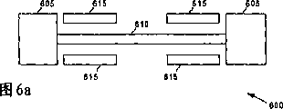
图6a和6b图解了根据本发明的一个优选实施例的爆炸阻挡体的备选形式;Figures 6a and 6b illustrate alternative forms of detonation barriers according to a preferred embodiment of the present invention;
图7a到7c图解了根据本发明的一个优选实施例的可熔断连接的备选实施例。Figures 7a to 7c illustrate an alternative embodiment of a fusible link according to a preferred embodiment of the present invention.
具体实施方式Detailed ways
下面详细描述各种实施例的制造和使用。但是,应当理解,本发明提供了许多可应用的发明概念,它们可以在许多特定的上下文环境中被具体实现。这里所描述的具体实施例只是用于解释制造和使用本发明的个别方式,并不是要限制本发明的范围。The making and using of various embodiments are described in detail below. It should be appreciated, however, that the present invention provides many applicable inventive concepts that can be embodied in many specific contexts. The specific embodiments described herein are intended merely to illustrate individual ways to make and use the invention, and are not intended to limit the scope of the invention.
现在看图1,该图图示了硬电介质层115上的非钝化激光熔丝100的俯视图。该硬电介质层在一个衬底116(图1a未图示,但是存在于后面的剖面图中)的顶部。如前所述,非钝化激光熔丝与钝化激光熔丝的不同之处在于前者缺乏保护其不受环境影响的钝化层。与钝化激光熔丝相比,非钝化激光熔丝的熔断所需的激光能量更少。这是由于在激光能够熔断激光熔丝之前,激光不必首先透过钝化层。进而,当暴露于激光的材料吸收激光能量时,更高能量激光的使用产生更大量的热。对于特定种类的材料,比如特殊的低k(介电常数)材料(例如由有机物质与硅的组合制造的衬底),对热相对来说敏感一些,一般不能承受熔断钝化激光熔丝时的过量热量,所述材料也不能承受与钝化激光熔丝的熔断相关联的机械应力。另外,诸如低k材料之类的材料的机械特性可能不是很适合承受迅速膨胀的蒸发熔丝材料所产生的压强。Turning now to FIG. 1 , this figure illustrates a top view of a
激光熔丝100的俯视图显示了激光熔丝的三个主要部分:允许将激光熔丝100电连接到电路和器件的两个焊盘105,以及可熔断连接110。在图示的实施例中,焊盘105物理上大于可熔断连接110。在备选实施例中,焊盘105和可熔断连接110的宽度可以相同(例如,熔丝看起来是单根线)。注意,尽管图示的可熔断连接110是直线,但是可熔断连接110可以形成为多种形状,比如之字形线、曲线、宽度和厚度变化的线等。焊盘105是线的允许将导电线连接到半导体器件的部分。The top view of the
可熔断连接110是激光熔丝的由激光加热而后断裂的部分。最好,所述两个焊盘105和可熔断连接110由同一种导电材料制成。可熔断连接110实际上可以用任何类型的金属制造,但是铝是优选的材料,这是因为铝的熔点相对较低,并且相对来说活性不高。另外,长久以来铝就是选用来进行半导体制造的金属。其它可以用于可熔断连接110的材料包括金,次一些的有铜和银。也可以使用各种合金,只要它们相对来说不易受腐蚀即可。Fusible link 110 is the portion of the laser fuse that is heated by the laser and then ruptures. Preferably, the two pads 105 and the fusible connection 110 are made of the same conductive material. Fusible link 110 may be fabricated from virtually any type of metal, but aluminum is the preferred material because of its relatively low melting point and is relatively inactive. In addition, aluminum has long been the metal of choice for semiconductor manufacturing. Other materials that may be used for the fusible link 110 include gold, to a lesser extent copper and silver. Various alloys can also be used as long as they are relatively insensitive to corrosion.
现在看图1b,该图图示了在图1a所示的衬底116顶部的硬介电层115上的激光熔丝100的剖视图,剖面沿着标为B-B的虚线。该剖视图图示了两个焊盘105具有穿过硬介电层115向下进入衬底116的导电通道,连接到用于电路和器件的连接点120。Turning now to FIG. 1b, this figure illustrates a cross-sectional view of the
现在看图1c,该图图示了按照线性方式布置的三个激光熔丝的熔丝阵列150。一般将激光熔丝安排为阵列,并安排得尽可能靠近,以使它们在集成电路中占据的表面积最小化。熔丝之间的间隔称为熔丝节距,熔丝节距被定义为熔丝的宽度加上两个相邻熔丝之间的间距。熔丝节距越小,熔丝就靠得越近。图1c中图示的熔丝阵列150具有三个激光熔丝(155、160和165),但是熔丝阵列可以有任意数量的熔丝组合在一起,对熔丝阵列中熔丝数量的约束是半导体表面区域的物理尺寸。Turning now to FIG. 1c, this figure illustrates a fuse array 150 of three laser fuses arranged in a linear fashion. Laser fuses are generally arranged in an array and placed as close together as possible to minimize the surface area they occupy in the integrated circuit. The spacing between fuses is called the fuse pitch, which is defined as the width of the fuse plus the spacing between two adjacent fuses. The smaller the fuse pitch, the closer the fuses are. The fuse array 150 illustrated in Fig. 1c has three laser fuses (155, 160 and 165), but the fuse array can have any number of fuses combined, the constraint on the number of fuses in the fuse array is The physical size of the surface area of a semiconductor.
熔丝可以以多种方式熔断。例如,电流就是熔断熔丝的另一种方式。但是,由于集成电路中多数器件和电路的精密性质,使用电流熔断可熔断连接的熔丝并不常用。也可以通过将熔丝暴露于辐射能而熔断熔丝。不论在什么情况下,本发明都能应用于以不同于使用激光的方式熔断的熔丝。Fuses can be blown in a number of ways. For example, electric current is another way to blow a fuse. However, due to the delicate nature of most devices and circuits in integrated circuits, the use of fuses for galvanically blown fusible links is not commonly used. The fuse can also be blown by exposing the fuse to radiant energy. In any case, the present invention can be applied to fuses that are blown in a manner other than using a laser.
激光熔丝使用激光加热并蒸发其可熔断连接。使用激光熔化然后切断可熔断连接是一样的,无论激光熔丝是钝化类型的还是非钝化类型的。对于钝化激光熔丝,激光在能够蒸发可熔断连接之前必须通过钝化层。这可以使用特定波长的激光实现,钝化层不吸收该波长的激光。例如,通常使用的钝化层SiO2允许特定波长的激光能量通过,而不会显著吸收激光能量。这样就能将激光能量集中用于熔断可熔断连接。Laser fuses use a laser to heat and vaporize their fusible link. Using a laser to melt and then sever the fusible link is the same, whether the laser fuse is a passivated or non-passivated type. For passivated laser fuses, the laser light must pass through the passivation layer before it can vaporize the fusible link. This can be achieved using a specific wavelength of laser light at which the passivation layer does not absorb. For example, the commonly used passivation layer SiO2 allows laser energy of a specific wavelength to pass through without significantly absorbing the laser energy. This allows laser energy to be focused on fusing the fusible link.
现在看图2a,该图图示了一个熔丝阵列200,其中,一个激光斑220被照射到激光熔丝205的可熔断连接上,用以熔断激光熔丝,可以通过将激光斑220的照射位置相对来说靠近可熔断连接的一端来熔断激光熔丝。这有助于在两个位置熔断激光熔丝的可熔断连接,每一个位置靠近可熔断连接的一个端部。Referring now to Fig. 2a, this figure illustrates a fuse array 200, wherein, a laser spot 220 is irradiated on the fusible link of
如前所述,通过激光斑220的加热作用熔断所述可熔断连接。首先,可熔断连接的熔丝材料被熔化,然后蒸发。熔化和蒸发过程的持续时间极其短暂,以防止热量的过度积聚。基本上,在热量弥散到熔丝连接区域之外的区域之前熔断过程就结束了。因此,熔丝材料的熔化和蒸发常常类似于爆炸:被激光斑220照射的熔丝材料实际上爆炸开来。As before, the fusible link is fused by the heating action of the laser spot 220 . First, the fuse material of the fusible link is melted and then evaporated. The duration of the melting and evaporation process is extremely short to prevent excessive build-up of heat. Basically, the fusing process is over before the heat dissipates to areas outside the fuse link area. Thus, the melting and vaporization of the fuse material is often similar to an explosion: the fuse material illuminated by the laser spot 220 actually explodes.
如前所述,如果激光熔丝是钝化激光熔丝类型的,则爆炸产生的碎屑很有可能不导致任何问题,这有两个可能的原因:第一个原因是钝化层提供了有效的保护,因为它覆盖了相邻熔丝的表面;第二个原因是钝化层困住了熔化的熔丝材料,直到其完全蒸发,蒸发的熔丝材料产生的碎屑往往是非导电的,因为其分散到了很大的区域上。但是,对于非钝化激光熔丝,熔化的熔丝材料不受约束,可能在熔化状态下就被射出。如果熔丝材料在熔化状态下被射出,其分散程度不足以使其不导电。因此,碎屑可能导致短路。取决于碎屑落在什么地方,靠近被熔断的熔丝的激光熔丝可能对其自身造成短路(在相邻熔丝此前已被熔断时出现的问题),或者相邻激光熔丝可能相互电短路。As mentioned earlier, if the laser fuse is a passivated laser fuse type, there is a good chance that the debris from the explosion will not cause any problems. There are two possible reasons for this: The first reason is that the passivation layer provides Effective protection because it covers the surface of the adjacent fuse; the second reason is that the passivation layer traps the molten fuse material until it evaporates completely, and the debris produced by the evaporated fuse material tends to be non-conductive , because it spreads over a large area. However, with non-passivated laser fuses, the molten fuse material is unconstrained and may be ejected in the molten state. If the fuse material is ejected in the molten state, it is not dispersed enough to render it non-conductive. Therefore, debris may cause a short circuit. Depending on where the debris lands, a laser fuse close to a blown fuse may short itself (a problem that occurs when adjacent fuses have been previously blown), or adjacent laser fuses may be electrically connected to each other. short circuit.
现在看图2b,该图图示了一个熔丝阵列250,其中第一激光熔丝205已被激光熔断,该熔断操作产生的碎屑(例如熔丝材料255的碎片)使得激光熔丝210与第一激光熔丝205电短路。例如,从第一激光熔丝205的可熔断连接的熔化的熔丝材料射出的熔丝材料碎片255在第一激光熔丝205和相邻激光熔丝210之间形成了一个电桥,将两个激光熔丝短接在一起。由于每一个激光熔丝连接点不同的电路,包含被短接的激光熔丝的集成电路很有可能不能正常工作,因此要被废弃。Referring now to FIG. 2b, this figure illustrates a
现在看图3a,根据本发明的一个优选实施例,该图图示了在衬底321(图3a中不可见,但是在后面的侧视图中进行了图示)的顶部的硬介电层320上的激光熔丝300的俯视图,其中,激光熔丝300具有内置爆炸阻挡体315,帮助防止熔化熔丝材料的溅射产生到相邻激光熔丝的电桥。所述爆炸屏蔽形成在可熔断连接310的每一侧,并且形成在在可熔断连接310的每一端,形成围绕可熔断连接310的将由激光烧灼的区域的水平包围。注意,如前所述,可熔断连接310尽管被图示为直线,但是其可以采用其它形式,比如之字线、曲线、可变宽度的线等。根据本发明的一个优选实施例,爆炸阻挡体315由与激光熔丝本身相同的材料形成。因此,爆炸阻挡体315可以在与激光熔丝相同的制造步骤中建立,从而不需要额外的制造步骤。但是,也可以用与集成电路的制造相容的任何其它类型的材料形成所述爆炸屏蔽315,包括用非导电材料制造。Turning now to FIG. 3a, this figure illustrates a
根据本发明的一个优选实施例,由于爆炸阻挡体315是用与激光熔丝相同的材料或者由任何导电材料制造的,在单个激光熔丝的每一端的爆炸阻挡体315必须不会相互接触。如果它们相互接触,则净效果就是产生了与所述可熔断连接并行的一个导电连接。如果爆炸阻挡体315是用非导电材料形成的,则单激光熔丝的爆炸阻挡体315可以被允许相互接触。另外,由于可以在衬底中在激光熔丝下方形成的通孔、沟道以及其它特征的缘故,可能不能形成沿着可熔断连接的整个长度的爆炸阻挡体。According to a preferred embodiment of the present invention, since the
现在看图3b和3c,它们图示了带有爆炸阻挡体315的激光熔丝300的侧视图(视角在水平面上方约45度),以及有三个激光熔丝355、360和365的熔丝阵列350的俯视图。根据本发明的一个优选实施例,由于爆炸阻挡体在形成激光熔丝的同一制造步骤中形成,爆炸阻挡体的高度会大致等于激光熔丝本身的高度。但是,如果爆炸阻挡体用不同的制造步骤形成,则爆炸阻挡体的高度可以被设置为使其效果最大化的高度。这意味着可以将爆炸阻挡体形成为与激光熔丝一样的高度,或者可以高于激光熔丝。注意,由于爆炸阻挡体的设计,阵列350的熔丝节距没有改变(与图1c显示的熔丝阵列150相比)。因此,可以设置与未受保护的激光熔丝的数量相仿的根据本发明制造的激光熔丝。Turning now to Figures 3b and 3c, they illustrate a side view (viewing angle approximately 45 degrees above horizontal) of
现在看图4a,该图图示了根据本发明的一个优选实施例的一个熔丝阵列400,其由具有爆炸阻挡体的熔丝构成,其中,已经在激光熔丝405的可熔断连接上照射了一个激光斑420,以烧断可熔断连接。紧紧围绕激光熔丝405的可熔断连接的是爆炸阻挡体406。注意,为了使爆炸阻挡体完全有效,爆炸阻挡体406应当延伸超过可熔断连接将被激光斑420蒸发的区域。如果爆炸阻挡体406不延伸超过可熔断连接要被蒸发的区域,则爆炸阻挡体的效果会被减损,未被爆炸阻挡体挡住的蒸发熔丝材料可能与其它激光熔丝形成电短路。Turning now to FIG. 4a, this figure illustrates a fuse array 400 according to a preferred embodiment of the present invention, which consists of fuses with detonation barriers, wherein the fusible links of laser fuses 405 have been irradiated A laser spot 420 is applied to blow the fusible link. Immediately surrounding the fusible link of the
现在看图4b,该图图示了根据本发明的一个优选实施例的熔丝阵列450,其中第一激光熔丝405已被激光熔断,熔断操作产生的碎屑(例如熔丝材料碎片455)被围绕第一激光熔丝405的爆炸阻挡体挡住。激光,例如激光斑420(图4a)对熔丝材料的蒸发形成的碎屑455一般会以不可预测的方式飞溅到不可预测的距离,在本实施例中则被约束到在第一激光熔丝405要被熔断的位置附近形成的爆炸阻挡体406内。爆炸阻挡体406形成围绕爆炸区的封闭,包住在熔丝熔断过程中射出的蒸发熔丝材料。Turning now to FIG. 4b, this figure illustrates a
根据本发明的一个优选实施例,爆炸阻挡体可以在形成激光熔丝的同一制造步骤中形成,并用与熔丝相同的材料形成。或者,爆炸阻挡体可以用与制造集成电路的制造工艺相容的任何材料制成。如果要使用额外的制造步骤来形成所述爆炸阻挡体,则所述爆炸熔丝最好由不导电的材料制成。According to a preferred embodiment of the present invention, the detonation barrier can be formed in the same manufacturing step as the laser fuse and be formed of the same material as the fuse. Alternatively, the explosion barrier may be made of any material compatible with the fabrication process used to manufacture integrated circuits. If an additional manufacturing step is to be used to form the detonation barrier, the detonation fuse is preferably made of a non-conductive material.
现在看图5,该图图示了根据本发明的一个优选实施例,带有L形的爆炸阻挡体的激光熔丝500。所述爆炸阻挡体515被形成为L形,该L形的从焊盘延伸出来的较长部分和较短的垂直部分形成一个对可熔断连接510的要熔断部分的更为完整的封闭。注意,如果爆炸阻挡体515是由导电材料(比如熔丝材料本身)形成的,则不应允许它接触可熔断连接510,除非在一端(比如通过焊盘505)。或者,爆炸阻挡体可以形成为在完全封闭可熔断连接的要熔断部分方面同样有效的其它形状。Turning now to FIG. 5, this figure illustrates a
现在看图6a和6b,其中图示了根据本发明的一个优选实施例的带有爆炸阻挡体的激光熔丝的替换实施例。在图6a中,图示了带有爆炸阻挡体的激光熔丝600,该爆炸阻挡体615不电耦接到焊盘605或者可熔断连接610,爆炸阻挡体615自身也没有电耦接(也就是,爆炸阻挡体的围绕激光熔丝600的一端的部分,以及爆炸阻挡体的围绕另一端的部分,不相耦接)。而在图6b中,图示的激光熔丝650的爆炸阻挡体665不与焊盘655或者可熔断连接660电耦接,但是爆炸阻挡体665形成为单一部件,保护可熔断连接660的整个长度。Turning now to Figures 6a and 6b, there is illustrated an alternative embodiment of a laser fuse with an explosion barrier in accordance with a preferred embodiment of the present invention. In FIG. 6a, a
现在看图7a到7c,图中图示了根据本发明的优选实施例的可熔断连接的备选实施例。在图7a中,图示了之字线形的可熔断连接710,而在图7b中图示了曲线形状的可熔断连接720。最后,在图7c中,图示了宽度变化的线形的可熔断连接730。可熔断连接的结构还可以有其它的实施例,其最终形状受约束条件的支配,所述约束条件比如是所希望的电阻率、承载的最大电流量、下伏衬底的构形等。Referring now to Figures 7a to 7c, there is illustrated an alternative embodiment of a fusible link in accordance with a preferred embodiment of the present invention. In Fig. 7a, a zigzag-shaped
根据本发明的另一种优选实施例,爆炸阻挡体的高度等于激光熔丝的高度。但是,爆炸阻挡体的高度可以变化,使得其高度可以大于或者小于激光熔丝的高度,以便更有效地围住蒸发的爆炸材料。According to another preferred embodiment of the present invention, the height of the explosion barrier is equal to the height of the laser fuse. However, the height of the detonation barrier can be varied such that it can be greater or lesser than the height of the laser fuse in order to more effectively enclose the evaporated detonation material.
尽管上面结合说明性的实施例对本发明进行了描述,但是上述说不应被解释为限制性的。上述说明性的实施例的各种变化和组合,以及本发明的其它实施例,对于阅读本说明书的本领域普通技术人员来所都是显而易见的。因此,所附的权利要求的范围不可任何这样的修改或者实施例。While the invention has been described in conjunction with illustrative embodiments, the foregoing should not be construed as limiting. Various modifications and combinations of the illustrative embodiments described above, as well as other embodiments of the invention, will be apparent to persons of ordinary skill in the art from reading this specification. Accordingly, the scope of the appended claims shall not be subjected to any such modifications or embodiments.
Claims (26)
Applications Claiming Priority (2)
| Application Number | Priority Date | Filing Date | Title |
|---|---|---|---|
| US10/246,999 | 2002-09-19 | ||
| US10/246,999 US6872648B2 (en) | 2002-09-19 | 2002-09-19 | Reduced splattering of unpassivated laser fuses |
Publications (2)
| Publication Number | Publication Date |
|---|---|
| CN1723552A true CN1723552A (en) | 2006-01-18 |
| CN100421232C CN100421232C (en) | 2008-09-24 |
Family
ID=31946432
Family Applications (1)
| Application Number | Title | Priority Date | Filing Date |
|---|---|---|---|
| CNB038222558A Expired - Lifetime CN100421232C (en) | 2002-09-19 | 2003-09-19 | Semiconductor device with reduced splattering of unpassivated laser fuses and method of manufacturing the same |
Country Status (7)
| Country | Link |
|---|---|
| US (1) | US6872648B2 (en) |
| EP (2) | EP1401018A3 (en) |
| JP (1) | JP5132033B2 (en) |
| KR (1) | KR100724510B1 (en) |
| CN (1) | CN100421232C (en) |
| AU (1) | AU2003278847A1 (en) |
| WO (1) | WO2004027801A2 (en) |
Cited By (3)
| Publication number | Priority date | Publication date | Assignee | Title |
|---|---|---|---|---|
| CN105518820A (en) * | 2013-08-28 | 2016-04-20 | 迪睿合株式会社 | Fuse element and fuse unit |
| CN112510118A (en) * | 2020-12-15 | 2021-03-16 | 东方日升新能源股份有限公司 | Photovoltaic cell slice welding method and photovoltaic cell assembly |
| CN114078812A (en) * | 2020-08-18 | 2022-02-22 | 上海华力微电子有限公司 | Electric programmable fuse unit layout structure |
Families Citing this family (18)
| Publication number | Priority date | Publication date | Assignee | Title |
|---|---|---|---|---|
| JP4795631B2 (en) | 2003-08-07 | 2011-10-19 | ルネサスエレクトロニクス株式会社 | Semiconductor device |
| JP4880950B2 (en) * | 2005-09-05 | 2012-02-22 | ルネサスエレクトロニクス株式会社 | Semiconductor device |
| JP2007243075A (en) * | 2006-03-10 | 2007-09-20 | Ricoh Co Ltd | Semiconductor device |
| US7492046B2 (en) * | 2006-04-21 | 2009-02-17 | International Business Machines Corporation | Electric fuses using CNTs (carbon nanotubes) |
| JP4903015B2 (en) * | 2006-06-06 | 2012-03-21 | ルネサスエレクトロニクス株式会社 | Semiconductor device, method for cutting electric fuse, and method for determining electric fuse |
| KR100799737B1 (en) * | 2006-06-16 | 2008-02-01 | 삼성전자주식회사 | Fuse structure and its formation method |
| JP5132162B2 (en) * | 2006-08-11 | 2013-01-30 | ルネサスエレクトロニクス株式会社 | Semiconductor integrated circuit |
| JP4995512B2 (en) * | 2006-08-23 | 2012-08-08 | ルネサスエレクトロニクス株式会社 | Semiconductor device |
| KR100979358B1 (en) | 2008-03-28 | 2010-08-31 | 주식회사 하이닉스반도체 | Fuses Prevent Thermal Deterioration |
| KR101043841B1 (en) * | 2008-10-14 | 2011-06-22 | 주식회사 하이닉스반도체 | Fuses in Semiconductor Memory Devices |
| US20100213569A1 (en) * | 2009-02-20 | 2010-08-26 | Taiwan Semiconductor Manufacturing Company, Ltd. | Integrated circuits having fuses and systems thereof |
| US9892221B2 (en) * | 2009-02-20 | 2018-02-13 | Taiwan Semiconductor Manufacturing Company, Ltd. | Method and system of generating a layout including a fuse layout pattern |
| KR101139485B1 (en) * | 2009-03-09 | 2012-05-02 | 에스케이하이닉스 주식회사 | Fuse of semiconductor device and method for forming the same |
| US8236615B2 (en) * | 2009-11-25 | 2012-08-07 | International Business Machines Corporation | Passivation layer surface topography modifications for improved integrity in packaged assemblies |
| JP2011199063A (en) * | 2010-03-19 | 2011-10-06 | Fujitsu Semiconductor Ltd | Semiconductor device and method of manufacturing the same |
| US20120286390A1 (en) * | 2011-05-11 | 2012-11-15 | Kuei-Sheng Wu | Electrical fuse structure and method for fabricating the same |
| US9070687B2 (en) | 2013-06-28 | 2015-06-30 | Taiwan Semiconductor Manufacturing Co., Ltd. | Semiconductor device with self-protecting fuse |
| US11935844B2 (en) | 2020-12-31 | 2024-03-19 | Texas Instruments Incorporated | Semiconductor device and method of the same |
Family Cites Families (12)
| Publication number | Priority date | Publication date | Assignee | Title |
|---|---|---|---|---|
| JP2728412B2 (en) | 1987-12-25 | 1998-03-18 | 株式会社日立製作所 | Semiconductor device |
| JP3256626B2 (en) * | 1994-05-15 | 2002-02-12 | 株式会社東芝 | Semiconductor device |
| US5567643A (en) * | 1994-05-31 | 1996-10-22 | Taiwan Semiconductor Manufacturing Company | Method of forming contamination guard ring for semiconductor integrated circuit applications |
| JP3224960B2 (en) * | 1994-12-15 | 2001-11-05 | 株式会社東芝 | Semiconductor device |
| US5608257A (en) * | 1995-06-07 | 1997-03-04 | International Business Machines Corporation | Fuse element for effective laser blow in an integrated circuit device |
| US5733806A (en) * | 1995-09-05 | 1998-03-31 | Motorola, Inc. | Method for forming a self-aligned semiconductor device |
| KR100190100B1 (en) * | 1996-10-16 | 1999-06-01 | 윤종용 | Semiconductor device |
| JP3186664B2 (en) * | 1997-09-19 | 2001-07-11 | 日本電気株式会社 | Semiconductor device and method of manufacturing the same |
| US6060398A (en) * | 1998-03-09 | 2000-05-09 | Siemens Aktiengesellschaft | Guard cell for etching |
| JPH11274304A (en) | 1998-03-25 | 1999-10-08 | Nkk Corp | Metal fuse element with dummy wiring |
| US6486526B1 (en) * | 1999-01-04 | 2002-11-26 | International Business Machines Corporation | Crack stop between neighboring fuses for protection from fuse blow damage |
| JP2001230325A (en) * | 2000-02-16 | 2001-08-24 | Oki Electric Ind Co Ltd | Metal fuse, manufacturing method thereof and mask |
-
2002
- 2002-09-19 US US10/246,999 patent/US6872648B2/en not_active Expired - Lifetime
-
2003
- 2003-09-18 EP EP03021103A patent/EP1401018A3/en not_active Withdrawn
- 2003-09-19 WO PCT/US2003/029595 patent/WO2004027801A2/en not_active Ceased
- 2003-09-19 EP EP03770364A patent/EP1547144A4/en not_active Withdrawn
- 2003-09-19 JP JP2004538285A patent/JP5132033B2/en not_active Expired - Fee Related
- 2003-09-19 CN CNB038222558A patent/CN100421232C/en not_active Expired - Lifetime
- 2003-09-19 AU AU2003278847A patent/AU2003278847A1/en not_active Abandoned
- 2003-09-19 KR KR1020057003952A patent/KR100724510B1/en not_active Expired - Fee Related
Cited By (3)
| Publication number | Priority date | Publication date | Assignee | Title |
|---|---|---|---|---|
| CN105518820A (en) * | 2013-08-28 | 2016-04-20 | 迪睿合株式会社 | Fuse element and fuse unit |
| CN114078812A (en) * | 2020-08-18 | 2022-02-22 | 上海华力微电子有限公司 | Electric programmable fuse unit layout structure |
| CN112510118A (en) * | 2020-12-15 | 2021-03-16 | 东方日升新能源股份有限公司 | Photovoltaic cell slice welding method and photovoltaic cell assembly |
Also Published As
| Publication number | Publication date |
|---|---|
| KR20050057262A (en) | 2005-06-16 |
| AU2003278847A1 (en) | 2004-04-08 |
| WO2004027801A2 (en) | 2004-04-01 |
| JP5132033B2 (en) | 2013-01-30 |
| EP1547144A2 (en) | 2005-06-29 |
| JP2006507668A (en) | 2006-03-02 |
| EP1401018A2 (en) | 2004-03-24 |
| US20040056322A1 (en) | 2004-03-25 |
| KR100724510B1 (en) | 2007-06-07 |
| EP1401018A3 (en) | 2004-09-08 |
| WO2004027801A3 (en) | 2005-02-24 |
| AU2003278847A8 (en) | 2004-04-08 |
| EP1547144A4 (en) | 2009-01-07 |
| US6872648B2 (en) | 2005-03-29 |
| CN100421232C (en) | 2008-09-24 |
Similar Documents
| Publication | Publication Date | Title |
|---|---|---|
| CN100421232C (en) | Semiconductor device with reduced splattering of unpassivated laser fuses and method of manufacturing the same | |
| US5523253A (en) | Array protection devices and fabrication method | |
| JP3968045B2 (en) | Fuse structure including cracking between adjacent fuses to protect against fuse blown damage | |
| US7867832B2 (en) | Electrical fuse and method of making | |
| US20040169578A1 (en) | Fuse component | |
| CN1547773A (en) | Optical and Electrically Programmable Siliconized Polysilicon Fuse Devices | |
| CN1139123C (en) | Fuse arrangement for improving technologic window of blowing fuses | |
| JP2010098024A (en) | Circuit protecting component | |
| JP5331408B2 (en) | Semiconductor device | |
| US7537969B2 (en) | Fuse structure having reduced heat dissipation towards the substrate | |
| CN107123635B (en) | Semiconductor device and fuse cutting method | |
| TWI714713B (en) | Semiconductor device | |
| JPH0414246A (en) | Fuse | |
| JP4202077B2 (en) | Fuse cutting method | |
| KR100563513B1 (en) | Protection layer for laser blown fuses | |
| JP2023149347A (en) | Semiconductor device | |
| RU2166812C1 (en) | Film fuse | |
| TW527695B (en) | High reliability fuse structure |
Legal Events
| Date | Code | Title | Description |
|---|---|---|---|
| C06 | Publication | ||
| PB01 | Publication | ||
| C10 | Entry into substantive examination | ||
| SE01 | Entry into force of request for substantive examination | ||
| C14 | Grant of patent or utility model | ||
| GR01 | Patent grant | ||
| CX01 | Expiry of patent term | ||
| CX01 | Expiry of patent term |
Granted publication date: 20080924 |