CN1855352A - Electron beam excited fluorescence emitting device - Google Patents
Electron beam excited fluorescence emitting device Download PDFInfo
- Publication number
- CN1855352A CN1855352A CNA2006100841801A CN200610084180A CN1855352A CN 1855352 A CN1855352 A CN 1855352A CN A2006100841801 A CNA2006100841801 A CN A2006100841801A CN 200610084180 A CN200610084180 A CN 200610084180A CN 1855352 A CN1855352 A CN 1855352A
- Authority
- CN
- China
- Prior art keywords
- electron beam
- phosphor
- emitting device
- beam excited
- ain
- Prior art date
- Legal status (The legal status is an assumption and is not a legal conclusion. Google has not performed a legal analysis and makes no representation as to the accuracy of the status listed.)
- Granted
Links
Images


Classifications
-
- C—CHEMISTRY; METALLURGY
- C09—DYES; PAINTS; POLISHES; NATURAL RESINS; ADHESIVES; COMPOSITIONS NOT OTHERWISE PROVIDED FOR; APPLICATIONS OF MATERIALS NOT OTHERWISE PROVIDED FOR
- C09K—MATERIALS FOR MISCELLANEOUS APPLICATIONS, NOT PROVIDED FOR ELSEWHERE
- C09K11/00—Luminescent materials, e.g. electroluminescent or chemiluminescent
- C09K11/08—Luminescent materials, e.g. electroluminescent or chemiluminescent containing inorganic luminescent materials
- C09K11/0883—Arsenides; Nitrides; Phosphides
-
- C—CHEMISTRY; METALLURGY
- C09—DYES; PAINTS; POLISHES; NATURAL RESINS; ADHESIVES; COMPOSITIONS NOT OTHERWISE PROVIDED FOR; APPLICATIONS OF MATERIALS NOT OTHERWISE PROVIDED FOR
- C09K—MATERIALS FOR MISCELLANEOUS APPLICATIONS, NOT PROVIDED FOR ELSEWHERE
- C09K11/00—Luminescent materials, e.g. electroluminescent or chemiluminescent
- C09K11/08—Luminescent materials, e.g. electroluminescent or chemiluminescent containing inorganic luminescent materials
- C09K11/64—Luminescent materials, e.g. electroluminescent or chemiluminescent containing inorganic luminescent materials containing aluminium
- C09K11/641—Chalcogenides
- C09K11/642—Chalcogenides with zinc or cadmium
-
- C—CHEMISTRY; METALLURGY
- C09—DYES; PAINTS; POLISHES; NATURAL RESINS; ADHESIVES; COMPOSITIONS NOT OTHERWISE PROVIDED FOR; APPLICATIONS OF MATERIALS NOT OTHERWISE PROVIDED FOR
- C09K—MATERIALS FOR MISCELLANEOUS APPLICATIONS, NOT PROVIDED FOR ELSEWHERE
- C09K11/00—Luminescent materials, e.g. electroluminescent or chemiluminescent
- C09K11/08—Luminescent materials, e.g. electroluminescent or chemiluminescent containing inorganic luminescent materials
- C09K11/77—Luminescent materials, e.g. electroluminescent or chemiluminescent containing inorganic luminescent materials containing rare earth metals
- C09K11/7728—Luminescent materials, e.g. electroluminescent or chemiluminescent containing inorganic luminescent materials containing rare earth metals containing europium
- C09K11/77346—Aluminium Nitrides or Aluminium Oxynitrides
-
- C—CHEMISTRY; METALLURGY
- C09—DYES; PAINTS; POLISHES; NATURAL RESINS; ADHESIVES; COMPOSITIONS NOT OTHERWISE PROVIDED FOR; APPLICATIONS OF MATERIALS NOT OTHERWISE PROVIDED FOR
- C09K—MATERIALS FOR MISCELLANEOUS APPLICATIONS, NOT PROVIDED FOR ELSEWHERE
- C09K11/00—Luminescent materials, e.g. electroluminescent or chemiluminescent
- C09K11/08—Luminescent materials, e.g. electroluminescent or chemiluminescent containing inorganic luminescent materials
- C09K11/77—Luminescent materials, e.g. electroluminescent or chemiluminescent containing inorganic luminescent materials containing rare earth metals
- C09K11/7728—Luminescent materials, e.g. electroluminescent or chemiluminescent containing inorganic luminescent materials containing rare earth metals containing europium
- C09K11/77348—Silicon Aluminium Nitrides or Silicon Aluminium Oxynitrides
-
- H—ELECTRICITY
- H01—ELECTRIC ELEMENTS
- H01J—ELECTRIC DISCHARGE TUBES OR DISCHARGE LAMPS
- H01J1/00—Details of electrodes, of magnetic control means, of screens, or of the mounting or spacing thereof, common to two or more basic types of discharge tubes or lamps
- H01J1/54—Screens on or from which an image or pattern is formed, picked-up, converted, or stored; Luminescent coatings on vessels
- H01J1/62—Luminescent screens; Selection of materials for luminescent coatings on vessels
- H01J1/63—Luminescent screens; Selection of materials for luminescent coatings on vessels characterised by the luminescent material
-
- H—ELECTRICITY
- H01—ELECTRIC ELEMENTS
- H01J—ELECTRIC DISCHARGE TUBES OR DISCHARGE LAMPS
- H01J29/00—Details of cathode-ray tubes or of electron-beam tubes of the types covered by group H01J31/00
- H01J29/02—Electrodes; Screens; Mounting, supporting, spacing or insulating thereof
- H01J29/10—Screens on or from which an image or pattern is formed, picked up, converted or stored
- H01J29/18—Luminescent screens
- H01J29/20—Luminescent screens characterised by the luminescent material
Landscapes
- Chemical & Material Sciences (AREA)
- Inorganic Chemistry (AREA)
- Engineering & Computer Science (AREA)
- Materials Engineering (AREA)
- Organic Chemistry (AREA)
- Luminescent Compositions (AREA)
- Cathode-Ray Tubes And Fluorescent Screens For Display (AREA)
Abstract
本发明提供了一种使用通过电子束的轰击发光并具有极佳的发光寿命的荧光体的电子束激励荧光发射装置。该电子束激励荧光体包括由至少形成有铕、硅和氧的AIN晶体或AIN固溶体晶体制备的固溶体,该荧光体用结构式Eua AIb Sic Nd Oe表示,其中a+b+c+d+e=1,且a,b,c,d和e满足以下条件:0.00001≤a≤0.1;0.4≤b≤0.55;0.001≤c≤0.1;0.4≤d≤0.55;0.001≤e≤0.1。
The present invention provides an electron beam excited fluorescence emission device using a phosphor that emits light by bombardment of electron beams and has an excellent luminescence lifetime. The electron beam excited phosphor includes a solid solution prepared by at least europium, silicon and oxygen formed with AlN crystals or AlN solid solution crystals, and the phosphor is represented by the structural formula Eua AIb Sic Nd Oe, wherein a+b+c+d+e= 1, and a, b, c, d and e satisfy the following conditions: 0.00001≤a≤0.1; 0.4≤b≤0.55; 0.001≤c≤0.1; 0.4≤d≤0.55; 0.001≤e≤0.1.
Description
技术领域technical field
本发明通常涉及一种通过电子照射使用荧光体发射光的荧光发射装置,尤其涉及一种具有极佳的发光寿命并在50V和以上的驱动阳极电压下驱动的电子束激励荧光发射装置。The present invention generally relates to a fluorescent emitting device that emits light using a phosphor by electron irradiation, and more particularly, to an electron beam excited fluorescent emitting device that has excellent luminous lifetime and is driven at a driving anode voltage of 50V and above.
背景技术Background technique
通常在使用场发射阴极的场发射显示器(下文称为“FED”)和真空荧光显示器(下文称为“VFD”)领域,已经使用各种各样的荧光体来获得发光色彩。如通过电子束轰击激励的显示器中使用的发射蓝光的荧光体在日本专利公开第2003-55657号和日本专利公开第2004-285363号中是通常已知的。日本专利公开第2003-55657号披露了一种低速率电子束激励的发射蓝光的荧光体(Y,Ce)2O3·SiO2,其具有结构式为[(Y,Ce)2O3·nSiO2(其中0.4≤n<1.0)]。日本专利公开第2004-285363号披露了发射蓝光的ZnS:Ag和Al,ZnS:Ag荧光粉,即使在长时间使用下它也具有较少晶体缺陷并难于劣化。在日本专利公开第2004-285363号中披露的荧光体有效地保持了荧光体的亮度,并提高了冷阴极场发射显示器的可靠性和寿命。Generally in the field of field emission displays (hereinafter referred to as "FED") and vacuum fluorescent displays (hereinafter referred to as "VFD") using field emission cathodes, various phosphors have been used to obtain emission colors. Blue light-emitting phosphors as used in displays excited by electron beam bombardment are generally known in Japanese Patent Laid-Open No. 2003-55657 and Japanese Patent Laid-Open No. 2004-285363. Japanese Patent Publication No. 2003-55657 discloses a low-rate electron beam-excited blue-emitting phosphor (Y, Ce) 2 O 3 ·SiO 2 , which has the structural formula [(Y, Ce) 2 O 3 ·nSiO 2 (where 0.4≤n<1.0)]. Japanese Patent Laid-Open No. 2004-285363 discloses ZnS:Ag and Al, ZnS:Ag phosphors emitting blue light, which have fewer crystal defects and are difficult to deteriorate even under long-term use. The phosphor disclosed in Japanese Patent Laid-Open No. 2004-285363 effectively maintains the brightness of the phosphor and improves the reliability and lifetime of the cold cathode field emission display.
另一方面,用激励源诸如具有高能量的光或电子束照射常规荧光体以发出光。结果存在一个问题,由于高能的激励降低了荧光体的亮度。因此需要能减小亮度降低的荧光体。为了提供满足该需求的荧光体,日本专利公开第2004-277663号披露了发射蓝光的具有通式[(Si,Al)12(O,N)16]的α型塞隆(Sialon)荧光体。日本专利公开第2005-8794号披露了由结构式Ca0.25Ce0.25[(Si,Al)12(O,N)16]表示的α型塞隆荧光体。On the other hand, conventional phosphors are irradiated with an excitation source such as light with high energy or electron beams to emit light. As a result, there is a problem that the luminance of the phosphor is lowered due to high-energy excitation. Phosphors capable of reducing the decrease in luminance are therefore required. In order to provide a phosphor meeting this demand, Japanese Patent Laid-Open No. 2004-277663 discloses an α-type Sialon phosphor having a general formula [(Si,Al) 12 (O,N) 16 ] that emits blue light. Japanese Patent Laid-Open No. 2005-8794 discloses an α-sialon phosphor represented by the structural formula Ca 0.25 Ce 0.25 [(Si,Al) 12 (O,N) 16 ].
应该注意到日本专利公开第2003-55657号中披露的Y2SiO5:Ce荧光体在使用期间极大地降低了发光效率,当将它用在FED时,在RGB(红、绿和蓝)中尤其是蓝的劣化程度存在极大的差异。此外,使用寿命短并且失去色平衡。在大约3kV的驱动电压下激励的FED中,由于电子的贯穿深度,不太可能使用金属。It should be noted that the Y 2 SiO 5 :Ce phosphor disclosed in Japanese Patent Laid-Open No. 2003-55657 greatly reduces luminous efficiency during use, and when it is used in a FED, in RGB (red, green and blue) In particular, there is a huge difference in the degree of deterioration of blue. In addition, the service life is short and the color balance is lost. In a FED driven at a driving voltage of about 3 kV, metals are unlikely to be used due to the penetration depth of electrons.
如在日本专利公开第2004-285363号中披露的包含硫的如ZnS:Ag,Al的ZnS:Ag,Al荧光体在装置的发射性能和寿命方面并不令人满意,因为硫通过电子轰击而发散并污染电子源。ZnS:Ag, Al phosphors containing sulfur such as ZnS:Ag, Al disclosed in Japanese Patent Laid-Open No. 2004-285363 are not satisfactory in terms of emission performance and lifetime of the device because sulfur is destroyed by electron bombardment. Diverge and contaminate the electron source.
在日本专利公开第2004-277663号和第2005-8794号披露的塞隆荧光体中,没有披露如何将塞隆荧光体应用到诸如场发射装置等的荧光发射装置中。In the sialon phosphors disclosed in Japanese Patent Laid-Open Nos. 2004-277663 and 2005-8794, there is no disclosure on how to apply the sialon phosphors to fluorescent emission devices such as field emission devices.
发明内容Contents of the invention
考虑到以上所述的问题,得出本发明。本发明的一个目的是提供一种较少地降低亮度、在使用寿命上性能极佳并且不会损失色平衡的电子束激励荧光发射装置。The present invention has been arrived at in consideration of the problems described above. SUMMARY OF THE INVENTION An object of the present invention is to provide an electron beam excited fluorescent emitting device with less decrease in luminance, excellent performance in service life and no loss of color balance.
附图说明Description of drawings
通过阅读以下详细说明和附图,本发明的这些和其它目的、特征和优点将更加明显,其中:These and other objects, features and advantages of the present invention will become more apparent upon reading the following detailed description and accompanying drawings, in which:
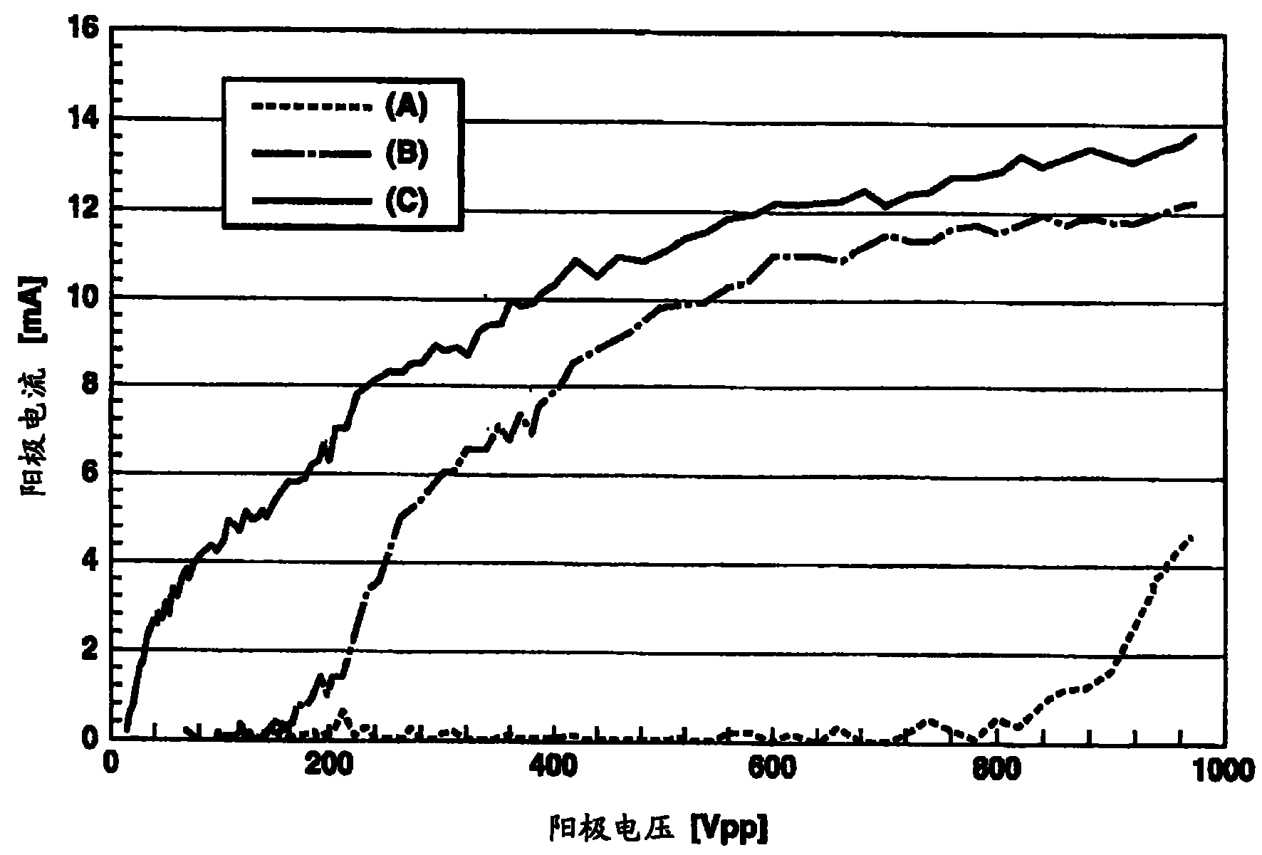
图1示出了在本发明的电子束激励荧光发射装置和现有技术的荧光发射装置之间阳极电流与阳极电压的比较图;Fig. 1 shows the comparison graph of anode current and anode voltage between the electron beam excited fluorescence emission device of the present invention and the prior art fluorescence emission device;
图2示出了在本发明的电子束激励荧光发射装置和现有技术的荧光发射装置之间发光效率的比较图;Fig. 2 shows a comparison diagram of luminous efficiency between the electron beam excited fluorescent emitting device of the present invention and the fluorescent emitting device of the prior art;
图3示出了在本发明的电子束激励荧光发射装置和现有技术的荧光发射装置之间发射性能的比较图;Fig. 3 shows a comparison diagram of the emission performance between the electron beam excited fluorescence emission device of the present invention and the fluorescence emission device of the prior art;
图4示出了在本发明的电子束激励荧光发射装置和现有技术的荧光发射装置之间色度变化率的表;和Fig. 4 shows a table of the chromaticity change rate between the electron beam excited fluorescent emitting device of the present invention and the fluorescent emitting device of the prior art; and
图5是FED的截面图。Fig. 5 is a cross-sectional view of the FED.
具体实施方式Detailed ways
以下将参照附图说明本发明的实施例。Embodiments of the present invention will be described below with reference to the drawings.
为了实现以上目的,本发明提供一种具有由电子束激励的荧光体的电子束激励荧光发射装置。该荧光体包括至少形成有铕、硅和氧的AlN晶体的固溶体或AIN固溶体晶体。将荧光体用电子束照射以发射具有波长为峰值在440nm到500nm之间的荧光。将AIN晶体或AIN固溶体晶体用结构式 Eua AIb Sic Nd Oe表示:In order to achieve the above object, the present invention provides an electron beam excited fluorescence emitting device having a phosphor excited by an electron beam. The phosphor includes a solid solution of AlN crystal or AlN solid solution crystal formed with at least europium, silicon and oxygen. The phosphor is irradiated with an electron beam to emit fluorescence having a peak wavelength between 440 nm and 500 nm. Use the structural formula of AIN crystal or AIN solid solution crystal Eua AIb Sic Nd Oe said:
其中a+b+c+d+e=1,且a,b,c,d和e满足以下条件:Where a+b+c+d+e=1, and a, b, c, d and e satisfy the following conditions:
0.00001≤a≤0.10.00001≤a≤0.1
0.4≤b≤0.550.4≤b≤0.55
0.001≤c≤0.10.001≤c≤0.1
0.4≤d≤0.550.4≤d≤0.55
0.001≤e≤0.10.001≤e≤0.1
AIN晶体或AIN固溶体晶体可以包含导电材料。AlN crystals or AlN solid solution crystals may contain conductive materials.
本发明的电子束激励荧光发射装置包括发射电子束的场发射源。可以将电子束从细丝状热电子发射源发出。The electron beam excited fluorescence emitting device of the present invention includes a field emission source that emits electron beams. An electron beam can be emitted from a filamentous thermionic emission source.
根据本发明的电子束激励荧光发射装置,在50V或以上的驱动电压下可以发射较少降低亮度并且在发光寿命优异的蓝光。当将本发明的电子束激励荧光发射装置用于如FED或VFD的显示器时,对发光寿命可以保持RGB(红、绿和蓝)的平衡并可以抑制RGB平衡的偏移。According to the electron beam excited fluorescence emission device of the present invention, it is possible to emit blue light with less decrease in luminance and excellent in luminous lifetime at a driving voltage of 50 V or more. When the electron beam excited fluorescent emitting device of the present invention is used for a display such as FED or VFD, the balance of RGB (red, green and blue) can be maintained and the shift of RGB balance can be suppressed for the luminescence lifetime.
本发明的电子束激励荧光发射装置包括作为主要成分的由铕活化的AIN晶体或AIN固溶体晶体(下文中称为“AIN:Eu”)。在将阳极电压设置成从几百V到几kV的场发射显示装置中使用多种荧光体的样品的试验结果中,本发明的发明人发现塞隆荧光体作为用于场发射显示装置的蓝光发射荧光体具有前途,因为它在高电压的电子轰击下难于发散。此外,本发明的发明人研究了发射蓝光的荧光体。结果产生了一个新的想法,即作为由铕活化的主晶的AIN晶体或AIN固溶体晶体可以用于荧光体。The electron beam excited fluorescence emitting device of the present invention includes AIN crystal or AIN solid solution crystal activated by europium (hereinafter referred to as "AIN:Eu") as a main component. In the test results of samples using various phosphors in a field emission display device in which the anode voltage was set from several hundred V to several kV, the inventors of the present invention found that the sialon phosphor was used as a blue light for field emission display devices. Emissive phosphors are promising because they are difficult to disperse under high voltage electron bombardment. Furthermore, the inventors of the present invention studied phosphors that emit blue light. As a result, a new idea has arisen that AIN crystals or AIN solid solution crystals as host crystals activated by europium can be used for phosphors.
AIN晶体是具有纤锌矿(wurtzite)型晶体结构的晶体。AIN固溶体晶体是把硅或氧加入AIN中形成的晶体。The AIN crystal is a crystal having a wurtzite type crystal structure. AlN solid solution crystal is a crystal formed by adding silicon or oxygen into AlN.
以下描述了AIN晶体或AIN固溶体晶体结构式的例子:Examples of crystal structural formulas of AlN crystals or AlN solid solutions are described below:
(1)2Hδ:Si2.40AI8.60O0.60N11.40 (1) 2Hδ: Si 2.40 AI 8.60 O 0.60 N 11.40
(2)27R:AI9O3N7:1AI2O3-7AIN(2)27R:AI 9 O 3 N 7 :1AI 2 O 3 -7AIN
(3)21R:AI7O3N5:1AI2O3-5AIN(3) 21R: AI 7 O 3 N 5 : 1AI 2 O 3 -5AIN
(4)12H:SiAI5O2N5:1SiO2-5AIN(4)12H:SiAI 5 O 2 N 5 :1SiO 2 -5AIN
(5)15R:SiAI4O2N4:1SiO2-4AIN(5) 15R: SiAI 4 O 2 N 4 : 1SiO 2 -4AIN
(6)8H:Si0.5AI3.5O2.5N2.5:0.5SiO2-0.5AI2O3-2.5AIN(6)8H: Si 0.5 AI 3.5 O 2.5 N 2.5 : 0.5SiO 2 -0.5AI 2 O 3 -2.5AIN
在本发明中,可以将如上所述的晶体用作主晶。可以用X射线衍射或中子衍射识别AIN晶体或AIN固溶体晶体。除了表现为与纯AIN晶体或AIN固溶体晶体的衍射相同的物质外,通过把组成成分用另一种成分替换来改变其晶格常数的晶体属于本发明的一部分。只要它的基本衍射数据不变,具有缺陷结构、堆垛层错或长周期结构的纯AIN晶体或AIN固溶体晶体也属于本发明的一部分。In the present invention, crystals as described above can be used as host crystals. AIN crystals or AIN solid solution crystals can be identified by X-ray diffraction or neutron diffraction. A crystal whose lattice constant is changed by substituting a constituent component with another is part of the present invention, except for a substance that exhibits the same diffraction as a pure AIN crystal or an AIN solid solution crystal. As long as its basic diffraction data remains unchanged, pure AIN crystals or AIN solid solution crystals with defect structures, stacking faults or long-period structures are also part of the present invention.
本发明里,只要晶体具有塞隆晶体结构并包含铕、硅、铝、氧和氮,并不特别限定晶体成分的类型。然而可以通过结构式Eua AIb Sic Nd Oe得到具有高亮度的发射蓝光的荧光体In the present invention, the type of crystal composition is not particularly limited as long as the crystal has a sialon crystal structure and contains europium, silicon, aluminum, oxygen and nitrogen. However, a blue-emitting phosphor with high brightness can be obtained by the structural formula Eua AIb Sic Nd Oe
其中a+b+c+d+e=1,且a,b,c,d和e满足以下条件:Where a+b+c+d+e=1, and a, b, c, d and e satisfy the following conditions:
(1)0.00001≤a≤0.1(1) 0.00001≤a≤0.1
(2)0.4≤b≤0.55(2) 0.4≤b≤0.55
(3)0.001≤c≤0.1(3) 0.001≤c≤0.1
(4)0.4≤d≤0.55(4) 0.4≤d≤0.55
(5)0.001≤e≤0.1(5) 0.001≤e≤0.1
结构式中“a”表示元素铕的加入量,并优选地将它设置成原子比为0.00001≤a≤0.1。当“a”的值小于0.00001时,因为作为发光中心的Eu的数量少,所以发射亮度降低。但“a”的值大于0.1时,因为由于铕离子的光学干涉而发生密度消光(extinction),也使发光亮度降低。"a" in the formula represents the added amount of element europium, and it is preferably set so that the atomic ratio is 0.00001≤a≤0.1. When the value of "a" is less than 0.00001, since the number of Eu as the luminescent center is small, the emission luminance decreases. However, when the value of "a" is larger than 0.1, the luminance of light emission is also lowered because of density extinction due to optical interference of europium ions.
结构式中“b”表示构成主晶的铝的量,并优选地将它设置成原子比为0.4≤b≤0.5。当“b”的值超过该范围时,晶体内的键变得不稳定,导致除AIN晶体或AIN固溶体晶体之外的晶相的产生率增加,这导致发射强度降低。"b" in the formula represents the amount of aluminum constituting the main crystal, and it is preferably set so that the atomic ratio is 0.4≤b≤0.5. When the value of "b" exceeds this range, bonds within the crystal become unstable, resulting in an increased generation rate of crystal phases other than AIN crystals or AIN solid solution crystals, which leads to a decrease in emission intensity.
结构式中“c”表示硅的量,并优选地将它设置成原子比为0.001≤a≤0.1。当“c”的值小于0.001时,电荷补偿效应变小,包含铕和氧的AIN晶体或AIN固溶体晶体的形成被抑制并且降低发射强度。"c" in the formula represents the amount of silicon, and it is preferably set so that the atomic ratio is 0.001≤a≤0.1. When the value of "c" is less than 0.001, the charge compensation effect becomes small, the formation of AlN crystals or AlN solid solution crystals containing europium and oxygen is suppressed and emission intensity is reduced.
结构式中“d”表示氮的量并优选地将它设置成原子比为0.4≤b≤0.55。当“d”的值超过该范围时,除了AIN晶体或AIN固溶体晶体之外的晶相的产生率增加,这导致发射强度降低。"d" in the formula represents the amount of nitrogen and it is preferably set so that the atomic ratio is 0.4≤b≤0.55. When the value of "d" exceeds this range, the generation rate of crystal phases other than AlN crystals or AlN solid solution crystals increases, which leads to a decrease in emission intensity.
结构式中“e”表示氧的量并优选地将它设置成原子比为0.001≤e≤0.1。当“e”的值小于0.001时,具有M的AIN晶体或AIN固溶体晶体的形成被抑制并且降低发射强度。当“e”的值大于0.1时,除了AIN固溶体晶体之外的晶相的产生率增加,这导致发射强度降低。"e" in the formula represents the amount of oxygen and it is preferably set so that the atomic ratio is 0.001≤e≤0.1. When the value of "e" is less than 0.001, the formation of AlN crystals or AlN solid solution crystals with M is suppressed and the emission intensity is reduced. When the value of "e" is larger than 0.1, the generation rate of crystal phases other than AlN solid solution crystals increases, which leads to a decrease in emission intensity.
下面将说明制备以上AIN:Eu荧光体的方法。应该认识到以下说明制备AIN:Eu荧光体的方法仅为示例而不限于此。A method of preparing the above AIN:Eu phosphor will be described below. It should be recognized that the method for preparing the AIN:Eu phosphor described below is only an example and is not limited thereto.
将具有0.5μm的平均粒径、0.93wt%氧含量和92%的α含量的氮化硅粉、具有3.3m2/g的比表面并且0.79%氧含量的氮化铝粉、以及具有99.9%纯度的氧化铕粉用作原始材料粉末。Silicon nitride powder with an average particle size of 0.5 μm, an oxygen content of 0.93 wt % and an α content of 92 %, an aluminum nitride powder with a specific surface area of 3.3 m 2 /g and an oxygen content of 0.79 %, and an aluminum nitride powder with an oxygen content of 99.9 % Pure europium oxide powder was used as the starting material powder.
为了得到由结构式Eu0.002845Al0.463253Si0.02845N0.501185O0.004267表示的化合物,使用烧结氮化硅制成的罐、烧结氮化铝制成的球和n-己烷(n-hexane),将6.389wt%的氮化硅粉、91.206%的氮化铝粉以及2.405wt%的氧化铕粉湿式球磨两个小时进行混合。In order to obtain the compound represented by the structural formula Eu 0.002845 Al 0.463253 Si 0.02845 N 0.501185 O 0.004267 , using a pot made of sintered silicon nitride, a ball made of sintered aluminum nitride and n-hexane (n-hexane), 6.389wt % silicon nitride powder, 91.206% aluminum nitride powder and 2.405 wt% europium oxide powder were mixed by wet ball milling for two hours.
通过旋转蒸发器去除n-己烷以得到混合粉末的干燥产物。将这样得到的混合粉末的干燥产物通过使用由玛瑙制成的研钵和研杵进行粉碎,并穿过500μm目的筛网以得到流度极佳的粉末集合。将粉末集合放入到氮化硼制成的具有20mm直径和20mm高度的坩埚内以得到30vol%的体积密度。根据填充的粉末集合的重量、坩锅的内部空间和粉末的实际密度(3.1g/cm3)来计算体积密度。n-Hexane was removed by rotary evaporator to obtain a dry product of mixed powder. The dried product of the mixed powder thus obtained was pulverized by using a mortar and pestle made of agate, and passed through a 500 μm-mesh sieve to obtain a powder assembly excellent in fluidity. The powder assembly was put into a crucible made of boron nitride having a diameter of 20 mm and a height of 20 mm to obtain a bulk density of 30 vol%. The bulk density was calculated from the weight of the filled powder assembly, the inner space of the crucible and the actual density of the powder (3.1 g/cm 3 ).
然后将坩锅置入石墨制成的电阻加热电炉。通过扩散泵抽空的用于煅烧的气氛来进行煅烧,将电熔炉以每小时500℃的速度从室温加热到800℃。在800℃温度下,将具有99.999vol%纯度的氮引入该气氛中以将气压设置到1M帕,并以每小时500℃的速度加热到2000℃,在2000℃保持2小时。The crucible was then placed in a resistance heating electric furnace made of graphite. Calcination was performed by an atmosphere for calcination evacuated by a diffusion pump, and the electric melting furnace was heated from room temperature to 800° C. at a rate of 500° C. per hour. At a temperature of 800° C., nitrogen with a purity of 99.999 vol % was introduced into the atmosphere to set the pressure to 1 M Pa, and heated to 2000° C. at a rate of 500° C. per hour, and kept at 2000° C. for 2 hours.
将这样合成的样品通过使用由玛瑙制成的研钵和研杵粉碎,通过使用铜的Kα线来进行粉末X射线衍射(XRD)测试。作为分析结果,确定生成具有纤锌矿型AIN结构的晶体。The sample thus synthesized was pulverized by using a mortar and pestle made of agate, and subjected to a powder X-ray diffraction (XRD) test by using Kα line of copper. As a result of the analysis, it was confirmed that crystals having a wurtzite-type AIN structure were generated.
通过使用如下文所述制备AIN:Eu荧光体来对VFD进行阴极发光亮度(CL)测定。Cathodoluminescence (CL) measurements were performed on VFDs by using AIN:Eu phosphors prepared as described below.
首先,将AIN:Eu荧光体混合到通过将乙基纤维素溶入到二甘醇二乙醚(由UCC制造的商标名为DEG单丁基醚)中制成的有机溶剂中以制备糊剂。然后通过使用该糊剂将荧光体沉积到阳极电极以制备VFD并测试。结果如图1所示,当施加大约800V或以上的阳极电压时,电流流过阳极,确定发射光(图1中线“A”)。为了比较,对Y2SiO5:Ce荧光体进行相同的测试。结果如图1所示,当阳极电压大约为150V时,电流流过阳极,确定发射光(图1中线“B”)。然后,将5wt%的氧化锌作为导电材料加入AIN:Eu荧光体中并测试。结果当阳极电流流动时的电压下降到大约100V,并确定发射光(图1中线“C”)。First, the AIN:Eu phosphor was mixed into an organic solvent prepared by dissolving ethyl cellulose in diethylene glycol diethyl ether (trade name DEG monobutyl ether manufactured by UCC) to prepare a paste. VFDs were then fabricated and tested by using the paste to deposit phosphors onto the anode electrode. As a result, as shown in FIG. 1 , when an anode voltage of about 800 V or more was applied, a current flowed through the anode, and light emission was confirmed (line "A" in FIG. 1 ). For comparison, the same test was performed on the Y 2 SiO 5 :Ce phosphor. As a result, as shown in FIG. 1, when the anode voltage was approximately 150V, the current flowed through the anode, and light was confirmed to be emitted (line "B" in FIG. 1). Then, 5wt% zinc oxide was added to the AIN:Eu phosphor as a conductive material and tested. As a result, the voltage when the anode current was flowing dropped to about 100 V, and it was confirmed that light was emitted (line "C" in Fig. 1).
接着,将5wt%的氧化锌作为导电材料加入AIN:Eu荧光体中以制备混合物。然后,将该混合物与通过将乙基纤维素溶入到二甘醇二乙醚(由UCC制造的商标名为DEG单丁基醚)中制成的有机溶剂混合以制备荧光体糊剂。接着通过使用该糊剂将荧光体沉积到阳极电极上以制备FFD,并在3kV的加速电压、1/240占空(duty)的脉冲驱动和8mA/cm2的电流密度的驱动条件下进行测试。Next, 5 wt% of zinc oxide was added as a conductive material to the AIN:Eu phosphor to prepare a mixture. Then, the mixture was mixed with an organic solvent prepared by dissolving ethyl cellulose into diethylene glycol diethyl ether (trade name DEG monobutyl ether manufactured by UCC) to prepare a phosphor paste. Next, FFD was prepared by using the paste to deposit phosphor onto the anode electrode, and tested under the driving conditions of an accelerating voltage of 3 kV, a pulse driving of 1/240 duty, and a current density of 8 mA/cm 2 .
图2示出了在以上条件下发光效率的半寿命周期的相对值。比较实例1是使用Y2SiO5:Ce荧光体的荧光发射装置。比较实例2中,使用了使用ZnS:Ag,AI荧光体的荧光发射装置,并将Y2SiO5:Ce荧光体用作为1.0的参考值。作为比较的结果,比较实例1是1.0且比较实例2是2.7,而本发明的实例是大约6.7。由这些结果可以确定本发明实例的发光效率寿命与比较实例1相比增长大约6.7倍,与比较实例2相比增长大约2.5倍。FIG. 2 shows relative values of the half-life cycles of luminous efficiency under the above conditions. Comparative Example 1 is a fluorescence emission device using a Y 2 SiO 5 :Ce phosphor. In Comparative Example 2, a fluorescence emission device using ZnS:Ag, AI phosphor was used, and Y 2 SiO 5 :Ce phosphor was used as a reference value of 1.0. As a result of the comparison, Comparative Example 1 was 1.0 and Comparative Example 2 was 2.7, while the Example of the present invention was about 6.7. From these results, it can be confirmed that the luminous efficiency lifetime of the examples of the present invention is increased by about 6.7 times compared with Comparative Example 1, and increased by about 2.5 times compared with Comparative Example 2.
图3示出了在与图2条件相同的条件下发射性能的半寿命周期的相对值。比较实例1是使用Y2SiO5:Ce荧光体的荧光发射装置。比较实例2中,使用了使用ZnS:Cu,AI荧光体的荧光发射装置,而将Y2SiO5:Ce荧光体用作为1.0的参考。作为比较的结果,比较实例1是1.0,比较实例2是0.19,本发明的实例是大约1.21。由这些结果可以确定本发明实例的发射寿命与比较实例1相比增长到大约1.21倍,与比较实例2相比增长大约6.4倍。FIG. 3 shows the relative value of the half-life cycle of emission performance under the same conditions as those in FIG. 2 . Comparative Example 1 is a fluorescence emission device using a Y 2 SiO 5 :Ce phosphor. In Comparative Example 2, a fluorescence emission device using ZnS:Cu, AI phosphor was used, and Y 2 SiO 5 :Ce phosphor was used as a reference of 1.0. As a result of the comparison, Comparative Example 1 was 1.0, Comparative Example 2 was 0.19, and the example of the present invention was about 1.21. From these results, it was confirmed that the emission lifetime of the inventive example was increased by about 1.21 times compared with Comparative Example 1, and increased by about 6.4 times compared with Comparative Example 2.
图4示出了在使用了2000小时后对FED全照明测试的色度量的改变。由图4确定,与使用Y2SiO5:Ce荧光体的比较实例1和与使用ZnS:Ag,AI荧光体的比较实例2相比较,本发明的荧光发射装置在色度上几乎没有变化并且在寿命稳定性上极佳。Figure 4 shows the change in chromaticity for the FED full illumination test after 2000 hours of use. As confirmed from FIG. 4 , compared with Comparative Example 1 using Y 2 SiO 5 :Ce phosphor and Comparative Example 2 using ZnS:Ag,AI phosphor, the fluorescence emitting device of the present invention has little change in chromaticity and Excellent in life stability.
将参照以下实例进一步说明本发明。然而应该认识到本发明并不旨在限制于这些实例,本领域技术人员在不脱离本发明精神和范围下可以进行修改和变动。The invention will be further illustrated with reference to the following examples. However, it should be understood that the present invention is not intended to be limited to these examples, and those skilled in the art may make modifications and changes without departing from the spirit and scope of the present invention.
实例1Example 1
图5示出了包括外壳的FED的结构,其包括彼此相对放置的阳极衬底1和阴极衬底2。将作为电子源的场发射阴极(FEC)3形成在阴极衬底2的内表面上,将发光阳极衬底4形成在与阴极衬底2相对的阳极衬底1的内表面上。FEC 3包括形成在阴极衬底2上的阴极导体5、形成在阴极导体5上的绝缘层6、形成在绝缘层6上的栅极7、形成在绝缘层6和栅极7中的孔8,和形成在孔8内阴极导体上的锥形发射器。阳极4包括透明导电膜10,例如作为阳极衬底1上阳极导体而形成的ITO,和沉积在透明导电膜10上的荧光体层11。从FEC 3发射的电子与荧光体层11碰撞以使它发出光。可以从阳极衬底1的外部通过可透射光的透明导体10和阳极衬底1看到荧光体11发出光。FIG. 5 shows the structure of a FED including a housing, which includes an anode substrate 1 and a
作为上文所述的FED中使用的荧光体,将作为导电介质的具有0.5μm粒径的5wt%氧化锌颗粒与用AIN:Eu荧光体表示的发射蓝光的荧光体混合,并在通过将乙基纤维素溶入到二甘醇二乙醚(由UCC制造的商标名为DEG单丁基醚)制成的有机溶剂中分散以制备糊剂。然后,将这样制备的荧光体糊剂应用到FED并测试其使用寿命性能。为了比较,通过使用Y2SiO5:Ce和ZnS:Ag,AI荧光体分别制备两种FED。将使用AIN:Eu荧光体、Y2SiO5:Ce荧光体和ZnS:Ag,AI荧光体形成的三种类型的FED在相同的条件下验证和测试。结果确定实例1与比较实例1和2相比寿命的稳定性极佳。As the phosphor used in the FED described above, 5 wt% zinc oxide particles having a particle diameter of 0.5 μm as a conductive medium were mixed with a blue light-emitting phosphor represented by an AIN:Eu phosphor, and the Base cellulose was dissolved in an organic solvent made of diethylene glycol diethyl ether (trade name DEG monobutyl ether manufactured by UCC) and dispersed to prepare a paste. Then, the thus-prepared phosphor paste was applied to FEDs and tested for lifetime performance. For comparison, two FEDs were prepared by using Y 2 SiO 5 :Ce and ZnS:Ag, AI phosphors, respectively. Three types of FEDs formed using AIN:Eu phosphor, Y 2 SiO 5 :Ce phosphor, and ZnS:Ag,AI phosphor were verified and tested under the same conditions. As a result, it was confirmed that Example 1 was excellent in stability of lifetime compared with Comparative Examples 1 and 2.
实例2Example 2
将作为导电介质的具有0.5μm粒径的5wt%氧化锌颗粒与用AIN:Eu荧光体表示的发射蓝光的荧光体混合,然后在包含乙基纤维素和丁基的有机溶剂中分散以制备糊剂。类似于实例1,将制备的荧光体糊剂应用到FED并测试其使用寿命性能。结果是与实例1所得到的效果相同。5 wt% zinc oxide particles having a particle diameter of 0.5 μm as a conductive medium were mixed with a blue light-emitting phosphor represented by AIN:Eu phosphor, and then dispersed in an organic solvent containing ethyl cellulose and butyl to prepare a paste agent. Similar to Example 1, the prepared phosphor paste was applied to FED and tested for lifetime performance. The result was the same effect as that obtained in Example 1.
实例3Example 3
将作为导电介质的具有0.5μm粒径的5wt%氧化锌颗粒与用AIN:Eu荧光体表示的发射蓝光的荧光体混合,并且然后在包含乙基纤维素和丁基的有机溶剂中分散以制备糊剂。然后通过使用这样制备的荧光体糊剂来制备VFD。当将50V电压施加到阳极电极时,得到具有实用亮度的蓝光发射。5 wt% zinc oxide particles having a particle diameter of 0.5 μm as a conductive medium were mixed with a blue light-emitting phosphor represented by AIN:Eu phosphor, and then dispersed in an organic solvent containing ethyl cellulose and butyl to prepare paste. A VFD was then prepared by using the phosphor paste thus prepared. When a voltage of 50 V was applied to the anode electrode, blue emission with practical brightness was obtained.
实例4Example 4
将作为导电介质的具有0.5μm粒径的5wt%氧化锌颗粒与用AIN:Eu荧光体表示的发射蓝光的荧光体混合,然后在包含乙基纤维素和丁基的有机溶剂中分散以制备糊剂。然后通过使用制备的荧光体糊剂来制备VFD。当将50V电压施加到阳极电极时,得到类似于实例3的具有实用亮度的蓝光发射。5 wt% zinc oxide particles having a particle diameter of 0.5 μm as a conductive medium were mixed with a blue light-emitting phosphor represented by AIN:Eu phosphor, and then dispersed in an organic solvent containing ethyl cellulose and butyl to prepare a paste agent. A VFD was then prepared by using the prepared phosphor paste. When a voltage of 50 V was applied to the anode electrode, blue light emission with practical brightness similar to Example 3 was obtained.
上述本发明的电子束激励荧光发射装置可以在50V和以上的驱动电压下发射蓝光且发光寿命极佳。当将本发明的电子束激励荧光发射装置用于诸如FED或VFD的显示器时,由于其发光寿命极佳,可以抑制RGB(红、绿和蓝)色平衡的偏移。The above-mentioned electron beam excited fluorescence emission device of the present invention can emit blue light at a driving voltage of 50V and above and has an excellent luminescence lifetime. When the electron beam excited fluorescent emitting device of the present invention is used for a display such as FED or VFD, it can suppress shift of RGB (red, green and blue) color balance due to its excellent luminous lifetime.
尽管已经以本发明具有一定具体性的优选方式进行了说明,但是应该认识到本发明不限于所提及的优选方式和附图。应该认识到本领域技术人员基于该方式作出其它技术的方式、实例和操作,都应该宽泛地解释为落入权利要求中所说明书的精神和范围内。Although the preferred modes of the invention have been described with some particularity, it should be understood that the invention is not limited to the preferred modes mentioned and the drawings. It should be recognized that the means, examples and operations of other technologies made by those skilled in the art based on the means should be broadly interpreted as falling within the spirit and scope of the claims.
Claims (8)
Applications Claiming Priority (2)
| Application Number | Priority Date | Filing Date | Title |
|---|---|---|---|
| JP2005113596A JP2006291035A (en) | 2005-04-11 | 2005-04-11 | Electron beam excited fluorescence device |
| JP113596/05 | 2005-04-11 |
Publications (2)
| Publication Number | Publication Date |
|---|---|
| CN1855352A true CN1855352A (en) | 2006-11-01 |
| CN1855352B CN1855352B (en) | 2010-06-02 |
Family
ID=37082548
Family Applications (1)
| Application Number | Title | Priority Date | Filing Date |
|---|---|---|---|
| CN2006100841801A Expired - Fee Related CN1855352B (en) | 2005-04-11 | 2006-04-11 | Electron beam pumped fluorescence emission device |
Country Status (4)
| Country | Link |
|---|---|
| US (1) | US7525245B2 (en) |
| JP (1) | JP2006291035A (en) |
| KR (1) | KR100787769B1 (en) |
| CN (1) | CN1855352B (en) |
Families Citing this family (12)
| Publication number | Priority date | Publication date | Assignee | Title |
|---|---|---|---|---|
| CN101018841B (en) * | 2004-08-11 | 2011-03-30 | 独立行政法人物质·材料研究机构 | Phosphor, its manufacturing method, and light-emitting device |
| US8114313B2 (en) | 2005-12-08 | 2012-02-14 | National Institute For Materials Science | Phosphor, process for producing the same, and luminescent device |
| JP4956732B2 (en) * | 2006-05-18 | 2012-06-20 | Dowaエレクトロニクス株式会社 | Phosphors and color display devices for electron beam excitation |
| JP5517400B2 (en) * | 2006-07-11 | 2014-06-11 | 日本碍子株式会社 | Blue light emitting aluminum nitride material and manufacturing method thereof |
| JP5322053B2 (en) * | 2007-01-12 | 2013-10-23 | 独立行政法人物質・材料研究機構 | Phosphor, method for producing the same, and light emitting device |
| EP2012343A3 (en) * | 2007-07-03 | 2010-09-08 | Fuji Jukogyo Kabushiki Kaisha | Light-emitting apparatus |
| JP2012519943A (en) * | 2009-03-10 | 2012-08-30 | オーシャンズ キング ライティング サイエンスアンドテクノロジー カンパニー リミテッド | White light emitting method and light emitting device |
| US8933526B2 (en) * | 2009-07-15 | 2015-01-13 | First Solar, Inc. | Nanostructured functional coatings and devices |
| GB2480265B (en) * | 2010-05-10 | 2013-10-02 | Toshiba Res Europ Ltd | A semiconductor device and a method of fabricating a semiconductor device |
| TWI458808B (en) * | 2011-08-26 | 2014-11-01 | Au Optronics Corp | Composition of phosphor, method of synthesizing the same, and electric device using the phosphor |
| CN106221695B (en) * | 2016-07-22 | 2019-05-07 | 成都理工大学 | Preparation method of aluminum nitride-based phosphor |
| US10600604B2 (en) | 2017-06-23 | 2020-03-24 | Current Lighting Solutions, Llc | Phosphor compositions and lighting apparatus thereof |
Family Cites Families (8)
| Publication number | Priority date | Publication date | Assignee | Title |
|---|---|---|---|---|
| NL8400660A (en) * | 1984-03-01 | 1985-10-01 | Philips Nv | LUMINESCENT SCREEN. |
| JP2003055657A (en) * | 2001-06-07 | 2003-02-26 | Nichia Chem Ind Ltd | Phosphor for slow electron beam |
| JP4366920B2 (en) * | 2002-11-07 | 2009-11-18 | ソニー株式会社 | Flat display device and manufacturing method thereof |
| JP2004277663A (en) * | 2003-03-18 | 2004-10-07 | National Institute For Materials Science | Sialon phosphor and manufacturing method thereof |
| JP3914987B2 (en) | 2003-06-20 | 2007-05-16 | 独立行政法人物質・材料研究機構 | Sialon phosphor and method for producing the same |
| JP4834827B2 (en) * | 2003-10-03 | 2011-12-14 | 独立行政法人物質・材料研究機構 | Oxynitride phosphor |
| JP2004285363A (en) | 2004-05-19 | 2004-10-14 | Sony Corp | Phosphor powder, method for producing the same, display panel, and flat display device |
| CN101018841B (en) * | 2004-08-11 | 2011-03-30 | 独立行政法人物质·材料研究机构 | Phosphor, its manufacturing method, and light-emitting device |
-
2005
- 2005-04-11 JP JP2005113596A patent/JP2006291035A/en active Pending
-
2006
- 2006-04-10 KR KR1020060032382A patent/KR100787769B1/en not_active Expired - Fee Related
- 2006-04-10 US US11/402,580 patent/US7525245B2/en not_active Expired - Fee Related
- 2006-04-11 CN CN2006100841801A patent/CN1855352B/en not_active Expired - Fee Related
Also Published As
| Publication number | Publication date |
|---|---|
| US20060226764A1 (en) | 2006-10-12 |
| KR20060107933A (en) | 2006-10-16 |
| US7525245B2 (en) | 2009-04-28 |
| KR100787769B1 (en) | 2007-12-24 |
| CN1855352B (en) | 2010-06-02 |
| JP2006291035A (en) | 2006-10-26 |
Similar Documents
| Publication | Publication Date | Title |
|---|---|---|
| CN101067080B (en) | Phosphor, its manufacturing method, and light-emitting device | |
| JP5586499B2 (en) | Method for manufacturing phosphor | |
| CN100526421C (en) | Phosphor, process for producing the same, lighting fixture and image display unit | |
| JP5322053B2 (en) | Phosphor, method for producing the same, and light emitting device | |
| JP5885174B2 (en) | Phosphor, method for manufacturing the same, light emitting device, and image display device | |
| CN1839192A (en) | Oxynitride phosphors and light emitting devices | |
| CN1249197C (en) | Green phosphorus and device using it | |
| CN1860205A (en) | Fluorescent substance, method for producing fluorescent substance, and light-emitting device using fluorescent substance | |
| CN1855352A (en) | Electron beam excited fluorescence emitting device | |
| JP4836229B2 (en) | Phosphor and light emitting device | |
| CN1497648A (en) | display device | |
| CN101389732A (en) | Phosphor for display device and field emission display device | |
| JP3918051B2 (en) | Mechanoluminescence material and method for producing the same | |
| JP6057231B2 (en) | Phosphor, light emitting device, image display device, pigment and ultraviolet absorber | |
| CN1680513A (en) | Fluorescent material and fluorescent display apparatus | |
| JP4173057B2 (en) | Fluorescent substance and fluorescent display device | |
| CN1550541A (en) | Phosphors for low-speed electron beams and fluorescent display tubes | |
| JP5170640B2 (en) | Phosphor, method for producing the same, and light emitting device | |
| CN1861744A (en) | Phosphor and fluorescent display device | |
| JP2006273929A (en) | Electron beam excitation phosphor and electron beam excitation fluorescent light emitting device | |
| CN1751109A (en) | Green light emitting phosphor for low voltage/high current density and field emissiion type display including the same | |
| WO2006129593A1 (en) | Phosphor for display and field emission display | |
| JP3942766B2 (en) | Phosphor | |
| CN1888012A (en) | Fluorescent RE Y3(Al, Ga)5O12 powder | |
| JP2005089496A (en) | Phosphor composition, method for producing the same and fluorescent display apparatus and method for emitting light using the same |
Legal Events
| Date | Code | Title | Description |
|---|---|---|---|
| C06 | Publication | ||
| PB01 | Publication | ||
| C10 | Entry into substantive examination | ||
| SE01 | Entry into force of request for substantive examination | ||
| C14 | Grant of patent or utility model | ||
| GR01 | Patent grant | ||
| CF01 | Termination of patent right due to non-payment of annual fee |
Granted publication date: 20100602 Termination date: 20180411 |
|
| CF01 | Termination of patent right due to non-payment of annual fee |