CN202004221U - Electric connector - Google Patents
Electric connector Download PDFInfo
- Publication number
- CN202004221U CN202004221U CN2010206333227U CN201020633322U CN202004221U CN 202004221 U CN202004221 U CN 202004221U CN 2010206333227 U CN2010206333227 U CN 2010206333227U CN 201020633322 U CN201020633322 U CN 201020633322U CN 202004221 U CN202004221 U CN 202004221U
- Authority
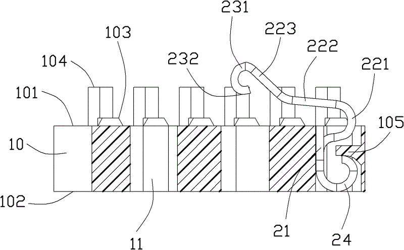
- CN
- China
- Prior art keywords
- contact portion
- contact
- elastic
- insulating body
- conductive terminal
- Prior art date
- Legal status (The legal status is an assumption and is not a legal conclusion. Google has not performed a legal analysis and makes no representation as to the accuracy of the status listed.)
- Expired - Fee Related
Links
Images


Landscapes
- Coupling Device And Connection With Printed Circuit (AREA)
- Connecting Device With Holders (AREA)
Abstract
本实用新型公开了一种电连接器,其包括绝缘本体及若干导电端子。导电端子具有固持在绝缘本体内的本体部、自本体部向上弯折延伸的弹性部、位于弹性部末端的接触部及自主体部向下延伸的安装部。接触部呈桶状,其先朝背离弹性部的方向延伸后再朝向弹性部弯折延伸,接触部的末端靠近弹性部形成有开口。导电端子发生轻微的变形即可使正压力急剧增加,从而保证其与芯片模组间的良好接触,而且同时满足了电连接器低构型的需求。
The utility model discloses an electric connector, which comprises an insulating body and a plurality of conductive terminals. The conductive terminal has a main body held in the insulating body, an elastic part bent upward from the main body, a contact part located at the end of the elastic part, and a mounting part extending downward from the main body. The contact part is in the shape of a barrel, which first extends away from the elastic part and then bends and extends towards the elastic part. An opening is formed at the end of the contact part close to the elastic part. A slight deformation of the conductive terminal can increase the positive pressure sharply, thereby ensuring a good contact between it and the chip module, and at the same time meeting the requirements of a low configuration of the electrical connector.
Description
【技术领域】【Technical field】
本实用新型关于一种电连接器,尤其涉及一种安装在电路板上用来连接芯片模组的电连接器。The utility model relates to an electric connector, in particular to an electric connector installed on a circuit board for connecting chip modules.
【背景技术】【Background technique】
CPU通常通过电连接器与印刷电路板电性连接,该种电连接器具有绝缘本体及安装在绝缘本体上的若干导电端子,导电端子具有与电路板连接的尾部及与CPU连接并可发生弹性变形的对接部。随着技术的不断发展,电连接器上导电端子排布密度不断增加,同时,电连接器的高度也随之降低,以满足小型化及薄型化的需求。The CPU is usually electrically connected to the printed circuit board through an electrical connector. This type of electrical connector has an insulating body and a number of conductive terminals mounted on the insulating body. The conductive terminals have tails connected to the circuit board and connected to the CPU and can be elastic. Deformed butt. With the continuous development of technology, the arrangement density of conductive terminals on the electrical connector is increasing, and at the same time, the height of the electrical connector is also reduced to meet the needs of miniaturization and thinning.
在通常的情形下,导电端子对接部的变形量与其可承受的正压力成正比,即对接部的变形量越大,其所能承受的正压力越大。而且,为实现导电端子与CPU间的良好电性连接,需要二者之间具有稳定的接触阻抗,因此必需相应增加导电端子的正压力。然而,据此设计时,需要使端子的弹性臂拉长,具有较好的弹性,进而具有较大的正压力,这样将无法有效降低导电端子的高度,而无法满足电连接器薄型化的需求。Under normal circumstances, the amount of deformation of the abutting portion of the conductive terminal is proportional to the normal pressure it can withstand, that is, the greater the deformation of the abutting portion, the greater the normal pressure it can withstand. Moreover, in order to achieve a good electrical connection between the conductive terminal and the CPU, it is necessary to have a stable contact resistance between the two, so it is necessary to increase the positive pressure of the conductive terminal accordingly. However, according to this design, the elastic arm of the terminal needs to be elongated to have better elasticity, and thus have a larger positive pressure, which will not be able to effectively reduce the height of the conductive terminal, and cannot meet the needs of thinning electrical connectors .
因此,有必要对前述电连接器进行改进以克服先前技术的缺陷。Therefore, it is necessary to improve the aforementioned electrical connectors to overcome the defects of the prior art.
【实用新型内容】【Content of utility model】
本实用新型的目的在于提供一种端子具有较大正压力的低构型电连接器。The purpose of the utility model is to provide a low-profile electrical connector with relatively large positive pressure on the terminals.
本实用新型的电连接器可通过以下技术方案实现:一种电连接器包括具有若干端子孔的绝缘本体及若干导电端子,导电端子具有卡持在绝缘本体端子孔内的本体部及与本体部一端连接的接触部。接触部具有相对设置的第一接触部及第二接触部,绝缘本体设有若干与导电端子的接触部相对应的挡止凸块,该挡止凸块与第二接触部接触。The electrical connector of the utility model can be realized through the following technical solutions: an electrical connector includes an insulating body with several terminal holes and a plurality of conductive terminals, and the conductive terminal has a body part and a body part that are clamped in the terminal holes of the insulating body. A contact part connected at one end. The contact portion has a first contact portion and a second contact portion oppositely arranged, and the insulating body is provided with a plurality of stop bumps corresponding to the contact portions of the conductive terminals, and the stop bumps are in contact with the second contact portion.
进一步地,导电端子的接触部呈桶状,接触部的末端具有开口。Further, the contact portion of the conductive terminal is barrel-shaped, and the end of the contact portion has an opening.
进一步地,所述挡止凸块自绝缘本体上表面向上延伸,所述第一接触部及第二接触部分别位于接触部的最高点及最低点。Further, the blocking protrusion extends upward from the upper surface of the insulating body, and the first contact portion and the second contact portion are respectively located at the highest point and the lowest point of the contact portion.
进一步地,接触部的末端自所述第二接触部向上延伸并在水平方向上穿过第一接触部。Further, the end of the contact portion extends upward from the second contact portion and passes through the first contact portion in a horizontal direction.
进一步地,导电端子具有位于本体部与接触部间的弹性部,弹性部向上弯折延伸出绝缘本体,接触部的开口靠近弹性部,弹性部包括与本体部相连的第一臂部、自第一臂部折弯并斜向上延伸的第二臂部及自第二臂部折弯并斜向上延伸的第三臂部,接触部与第三臂部相连接。Furthermore, the conductive terminal has an elastic portion located between the main body and the contact portion, the elastic portion is bent upwards and extends out of the insulating body, the opening of the contact portion is close to the elastic portion, the elastic portion includes a first arm connected to the main body, and a first arm connected to the main body. A second arm bent from one arm and extending obliquely upward, and a third arm bent from the second arm and extending obliquely upward, the contact portion is connected to the third arm.
进一步地,所述第一臂部为弯曲状,第二臂部及第三臂部为平直状,弹性部的第一臂部位于本体部的一侧,弹性部的第二臂部越过本体部,弹性部的第三臂部及接触部位于本体部的另一侧,弹性部的第一臂部延伸出绝缘本体,第二臂部、第三臂部及接触部位于绝缘本体外。Further, the first arm part is curved, the second arm part and the third arm part are straight, the first arm part of the elastic part is located on one side of the body part, and the second arm part of the elastic part goes over the body part part, the third arm part and the contact part of the elastic part are located on the other side of the body part, the first arm part of the elastic part extends out of the insulating body, and the second arm part, the third arm part and the contact part are located outside the insulating body.
进一步地,所述导电端子在绝缘本体上排成相互垂直的若干行与若干列,所述弹性部的延伸方向偏离这些行及这些列,一导电端子的接触部是延伸至另一导电端子的弹性部旁侧,所述另一导电端子位于该一导电端子的相邻行及相邻列上。Further, the conductive terminals are arranged in several rows and columns perpendicular to each other on the insulating body, the extending direction of the elastic portion deviates from these rows and these columns, and the contact portion of one conductive terminal extends to the other conductive terminal. Next to the elastic part, the other conductive terminal is located on the adjacent row and adjacent column of the one conductive terminal.
进一步地,在每一导电端子接触部及弹性部的旁侧于绝缘本体上还分别设有分隔凸块,分隔凸块将该导电端子与靠近的导电端子隔开,所述挡止凸块的高度小于分隔凸块的高度。Further, on the sides of each conductive terminal contact portion and the elastic portion, separate bumps are respectively provided on the insulating body, and the partition bumps separate the conductive terminals from the adjacent conductive terminals, and the stop bumps The height is less than the height of the separation bump.
进一步地,同一导电端子的接触部旁侧的分隔凸块与弹性部的旁侧的分隔凸块分别位于该导电端子的两侧。Further, the separation bumps on the side of the contact portion of the same conductive terminal and the separation bumps on the side of the elastic portion are respectively located on two sides of the conductive terminal.
进一步地,所述第一接触部及第二接触部分别位于接触部的最低点及最高点,接触部的末端的开口靠近本体部,所述挡止凸块位于绝缘本体内。Further, the first contact portion and the second contact portion are respectively located at the lowest point and the highest point of the contact portion, the opening at the end of the contact portion is close to the main body, and the stop bump is located in the insulating main body.
相较于先前技术,本实用新型导电端子的接触部与绝缘本体的挡止凸块接触后,导电端子发生轻微的变形即可使正压力急剧增加,从而保证其与芯片模组间的良好接触,降低二者间的接触阻抗,而且无需通过加长端子,同时满足了电连接器低构型的需求。Compared with the prior art, after the contact part of the conductive terminal of the utility model contacts the stop bump of the insulating body, the positive pressure can be sharply increased by a slight deformation of the conductive terminal, thereby ensuring good contact between it and the chip module , reduce the contact resistance between the two, and do not need to extend the terminal, and at the same time meet the requirements of the low configuration of the electrical connector.
【附图说明】【Description of drawings】
图1是本实用新型的电连接器的立体组合图。FIG. 1 is a three-dimensional assembled view of the electrical connector of the present invention.
图2是本实用新型的电连接器的立体分解图。Fig. 2 is a three-dimensional exploded view of the electrical connector of the present invention.
图3是本实用新型的电连接器的俯视图。Fig. 3 is a top view of the electrical connector of the present invention.
图4是本实用新型的电连接器的导电端子的侧视图。Fig. 4 is a side view of the conductive terminal of the electrical connector of the present invention.
图5是本实用新型的电连接器沿图3中A-A线的剖视图,图中仅显示了一个端子。Fig. 5 is a cross-sectional view of the electrical connector of the present invention along line A-A in Fig. 3, and only one terminal is shown in the figure.
图6是本实用新型的电连接器与芯片模组配合时的剖视图。Fig. 6 is a cross-sectional view of the electrical connector of the present invention when mated with the chip module.
【具体实施方式】【Detailed ways】
请参阅图1、图2及图6所示,本实用新型电连接器100用以电性连接芯片模组30及电路板(未图标),其包括绝缘本体10及若干导电端子20。绝缘本体10具有相对的上表面101、下表面102及若干贯穿绝缘本体10的端子孔11。绝缘本体10的上表面101在每一端子孔11旁侧设有挡止凸块103及位于挡止凸块103外侧的分隔凸块104,挡止凸块103低于分隔凸块104。端子孔11内还设有挡止凸块105。Please refer to FIG. 1 , FIG. 2 and FIG. 6 , the
请一并参阅图4所示,导电端子20具有卡持在绝缘本体10的端子孔11内的本体部21、自本体部21向上弯折延伸出绝缘本体10的弹性部22、位于弹性部22末端的接触部23及自本体部21向下延伸的安装部24。接触部23呈桶状,其先朝背离弹性部22的方向延伸后再朝向弹性部22延伸。接触部23在背离弹性部22延伸的同时先向上延伸形成位于最高点的第一接触部231,再进而向下延伸。然后,接触部再弯折向弹性部22,形成位于最低点的第二接触部232,接触部23的末端233自第二接触部232向上延伸并在水平方向上穿过最高点即第一接触部231。接触部23的末端233形成有靠近弹性部22的开口234。Please also refer to FIG. 4, the
请参阅图2及图4所示,弹性部22包括与本体部21相连的第一臂部221、自第一臂部221折弯并斜向上延伸的第二臂部222及自第二臂部222折弯并斜向上延伸的第三臂部223,接触部23与第三臂部223相连接。安装部24与弹性部22的第一臂部221位于本体部21的一侧,弹性部22的第二臂部222越过本体部21,弹性部22的第三臂部223及接触部23位于本体部21的另一侧。第一臂部221为弯曲状,第二臂部222及第三臂部223为平直状。弹性部22的第一臂部221延伸出绝缘本体10,第二臂部222、第三臂部223及接触部23位于绝缘本体10外。安装部24亦呈桶状。2 and 4, the
请参阅图3及图5所示,导电端子20在绝缘本体10上排成相互垂直的若干行与若干列,而导电端子20的弹性部22的延伸方向偏离这些行及这些列。导电端子20的接触部23是延伸至同时位于该导电端子20的相邻行及相邻列上的另一导电端子20的弹性部22旁侧。绝缘本体10的挡止凸块103位于相应的导电端子20的接触部23下方。绝缘本体10的分隔凸块104位于一个导电端子20的接触部23及位于该接触部23旁侧的另一导电端子20的弹性部22之间,以防止所述两个导电端子20的接触部23与弹性部22接触而发生短路。绝缘本体10的端子孔11内的挡止凸块105可与导电端子20的安装部24接触。Please refer to FIG. 3 and FIG. 5 , the
请参阅图1、图5及图6所示,当芯片模组30组装至电连接器100上时,芯片模组30的导电片(未标号)先与导电端子20的第一接触部231对接,并进一步下压导电端子20,从而使得导电端子20的弹性部22发生变形,带动接触部23向下运动直至第二接触部232与绝缘本体10的挡止凸块103接触。由于接触部23呈桶状且其具有一开口234,因此当其与挡止凸块103接触后,可发生轻微的变形,该轻微的变形可使芯片模组30下压的正压力急剧增加,从而保证二者间的良好接触。相较于现有的导电端子,本实用新型无需通过加长端子,导电端子20在发生微量变形的情形下即可产生较大的正压力,不但保证与芯片模组30间的稳定接触,降低二者间的接触阻抗;而且满足了电连接器低构型的需求。Please refer to FIG. 1 , FIG. 5 and FIG. 6 , when the chip module 30 is assembled on the
请参阅图5所示,当电连接器100安装至电路板上时,导电端子20是与电路板电性连接,在图1至图6所示的实施方式中,导电端子20的安装部24是采用面接触的方式与电路板结合,当然,也可以采用焊接的方式结合。由于安装部24呈桶状且与电路板之间采用面接触,其同样具有第一接触部(未标号)及第二接触部(未标号),此时第一接触部为位于最低点与电路板接触的部分,而第二接触部为位于最高点的部分。由于在绝缘本体10内设置有挡止凸块105,故挡止凸块105可与安装部24的第二接触部接触,从而使得安装部24也可以发生微量变形后提供足够的接触力。5, when the
请参阅图1及图3所示,为满足高密度的需求,本实用新型的导电端子20排布紧密,分属于不同导电端子20的接触部23与弹性部22之间距离较近,因此在绝缘本体10的上表面101上于不同导电端子20的接触部23与弹性部22之间设有分隔凸块104以防止二者接触。或者说,每一导电端子20的接触部23与弹性部22旁侧均设有分隔凸块104,且同一导电端子20的接触部23旁侧的分隔凸块104与弹性部22的旁侧的分隔凸块104分别设于该导电端子20的两侧,将该导电端子20与其它导电端子20隔开。通过此,可防止不同的导电端子20间相互接触,避免了短路现象的发生。Please refer to Fig. 1 and Fig. 3, in order to meet the requirement of high density, the
Claims (10)
Priority Applications (1)
| Application Number | Priority Date | Filing Date | Title |
|---|---|---|---|
| CN2010206333227U CN202004221U (en) | 2010-11-30 | 2010-11-30 | Electric connector |
Applications Claiming Priority (1)
| Application Number | Priority Date | Filing Date | Title |
|---|---|---|---|
| CN2010206333227U CN202004221U (en) | 2010-11-30 | 2010-11-30 | Electric connector |
Publications (1)
| Publication Number | Publication Date |
|---|---|
| CN202004221U true CN202004221U (en) | 2011-10-05 |
Family
ID=44706948
Family Applications (1)
| Application Number | Title | Priority Date | Filing Date |
|---|---|---|---|
| CN2010206333227U Expired - Fee Related CN202004221U (en) | 2010-11-30 | 2010-11-30 | Electric connector |
Country Status (1)
| Country | Link |
|---|---|
| CN (1) | CN202004221U (en) |
Cited By (4)
| Publication number | Priority date | Publication date | Assignee | Title |
|---|---|---|---|---|
| CN108336542A (en) * | 2017-06-23 | 2018-07-27 | 番禺得意精密电子工业有限公司 | Electric connector |
| CN108615999A (en) * | 2018-03-20 | 2018-10-02 | 番禺得意精密电子工业有限公司 | Electric connector |
| CN109037988A (en) * | 2017-05-12 | 2018-12-18 | 番禺得意精密电子工业有限公司 | Electric connector |
| CN110943317A (en) * | 2019-12-19 | 2020-03-31 | 富士康(昆山)电脑接插件有限公司 | Electrical connector |
-
2010
- 2010-11-30 CN CN2010206333227U patent/CN202004221U/en not_active Expired - Fee Related
Cited By (6)
| Publication number | Priority date | Publication date | Assignee | Title |
|---|---|---|---|---|
| CN109037988A (en) * | 2017-05-12 | 2018-12-18 | 番禺得意精密电子工业有限公司 | Electric connector |
| CN109037988B (en) * | 2017-05-12 | 2020-08-28 | 番禺得意精密电子工业有限公司 | Electrical connector |
| CN108336542A (en) * | 2017-06-23 | 2018-07-27 | 番禺得意精密电子工业有限公司 | Electric connector |
| CN108615999A (en) * | 2018-03-20 | 2018-10-02 | 番禺得意精密电子工业有限公司 | Electric connector |
| US10547137B2 (en) | 2018-03-20 | 2020-01-28 | Lotes Co., Ltd | Electrical connector |
| CN110943317A (en) * | 2019-12-19 | 2020-03-31 | 富士康(昆山)电脑接插件有限公司 | Electrical connector |
Similar Documents
| Publication | Publication Date | Title |
|---|---|---|
| US8172591B2 (en) | Electrical connector assembly having electrical connector with low profile and processor with cone pins | |
| US7791443B1 (en) | Electrical connector | |
| US7938649B2 (en) | Electrical connector having improved contacts | |
| CN201927733U (en) | Electrical connector | |
| US7780456B2 (en) | Electrical connector having reinforced contacts arrangement | |
| US8202100B2 (en) | Electrical connector connecting two board shaped device | |
| TWI506867B (en) | Electrical connector | |
| CN2757356Y (en) | Electric connector | |
| CN103579812A (en) | Electrical connector | |
| US8366452B2 (en) | Low profile socket connector with improved contacts | |
| CN202004221U (en) | Electric connector | |
| US20120225586A1 (en) | Electrical connector | |
| US8079857B2 (en) | Electrical connector with drainage channels | |
| US9130321B2 (en) | Electrical connector having contact for either BGA or LGA package | |
| CN202308486U (en) | Electric connector | |
| US8690585B2 (en) | Electrical connector for low profile application | |
| CN101154782B (en) | Electric connector and manufacturing method thereof | |
| US20140080330A1 (en) | Electrical contact and electrical connector used thereof | |
| CN103208707A (en) | Electric connector | |
| TWI446634B (en) | Electrical connector | |
| TW202215718A (en) | Electrical connector | |
| CN203445292U (en) | Electric connector and conductive terminal thereof | |
| CN201112663Y (en) | Electric connector | |
| CN201594598U (en) | electrical connector | |
| CN103579799B (en) | Electric connector |
Legal Events
| Date | Code | Title | Description |
|---|---|---|---|
| C14 | Grant of patent or utility model | ||
| GR01 | Patent grant | ||
| CF01 | Termination of patent right due to non-payment of annual fee | ||
| CF01 | Termination of patent right due to non-payment of annual fee |
Granted publication date: 20111005 Termination date: 20191130 |