CN86100902A - magneto-optical storage system - Google Patents
magneto-optical storage system Download PDFInfo
- Publication number
- CN86100902A CN86100902A CN86100902A CN86100902A CN86100902A CN 86100902 A CN86100902 A CN 86100902A CN 86100902 A CN86100902 A CN 86100902A CN 86100902 A CN86100902 A CN 86100902A CN 86100902 A CN86100902 A CN 86100902A
- Authority
- CN
- China
- Prior art keywords
- circuit
- signal
- sector
- header
- data
- Prior art date
- Legal status (The legal status is an assumption and is not a legal conclusion. Google has not performed a legal analysis and makes no representation as to the accuracy of the status listed.)
- Expired - Lifetime
Links
Images


Classifications
-
- G—PHYSICS
- G11—INFORMATION STORAGE
- G11B—INFORMATION STORAGE BASED ON RELATIVE MOVEMENT BETWEEN RECORD CARRIER AND TRANSDUCER
- G11B7/00—Recording or reproducing by optical means, e.g. recording using a thermal beam of optical radiation by modifying optical properties or the physical structure, reproducing using an optical beam at lower power by sensing optical properties; Record carriers therefor
- G11B7/24—Record carriers characterised by shape, structure or physical properties, or by the selection of the material
- G11B7/26—Apparatus or processes specially adapted for the manufacture of record carriers
-
- G—PHYSICS
- G11—INFORMATION STORAGE
- G11B—INFORMATION STORAGE BASED ON RELATIVE MOVEMENT BETWEEN RECORD CARRIER AND TRANSDUCER
- G11B27/00—Editing; Indexing; Addressing; Timing or synchronising; Monitoring; Measuring tape travel
- G11B27/10—Indexing; Addressing; Timing or synchronising; Measuring tape travel
- G11B27/19—Indexing; Addressing; Timing or synchronising; Measuring tape travel by using information detectable on the record carrier
- G11B27/28—Indexing; Addressing; Timing or synchronising; Measuring tape travel by using information detectable on the record carrier by using information signals recorded by the same method as the main recording
- G11B27/30—Indexing; Addressing; Timing or synchronising; Measuring tape travel by using information detectable on the record carrier by using information signals recorded by the same method as the main recording on the same track as the main recording
-
- G—PHYSICS
- G11—INFORMATION STORAGE
- G11B—INFORMATION STORAGE BASED ON RELATIVE MOVEMENT BETWEEN RECORD CARRIER AND TRANSDUCER
- G11B11/00—Recording on or reproducing from the same record carrier wherein for these two operations the methods are covered by different main groups of groups G11B3/00 - G11B7/00 or by different subgroups of group G11B9/00; Record carriers therefor
- G11B11/10—Recording on or reproducing from the same record carrier wherein for these two operations the methods are covered by different main groups of groups G11B3/00 - G11B7/00 or by different subgroups of group G11B9/00; Record carriers therefor using recording by magnetic means or other means for magnetisation or demagnetisation of a record carrier, e.g. light induced spin magnetisation; Demagnetisation by thermal or stress means in the presence or not of an orienting magnetic field
- G11B11/105—Recording on or reproducing from the same record carrier wherein for these two operations the methods are covered by different main groups of groups G11B3/00 - G11B7/00 or by different subgroups of group G11B9/00; Record carriers therefor using recording by magnetic means or other means for magnetisation or demagnetisation of a record carrier, e.g. light induced spin magnetisation; Demagnetisation by thermal or stress means in the presence or not of an orienting magnetic field using a beam of light or a magnetic field for recording by change of magnetisation and a beam of light for reproducing, i.e. magneto-optical, e.g. light-induced thermomagnetic recording, spin magnetisation recording, Kerr or Faraday effect reproducing
- G11B11/10595—Control of operating function
- G11B11/10597—Adaptations for transducing various formats on the same or different carriers
-
- G—PHYSICS
- G11—INFORMATION STORAGE
- G11B—INFORMATION STORAGE BASED ON RELATIVE MOVEMENT BETWEEN RECORD CARRIER AND TRANSDUCER
- G11B13/00—Recording simultaneously or selectively by methods covered by different main groups among G11B3/00, G11B5/00, G11B7/00 and G11B9/00; Record carriers therefor not otherwise provided for; Reproducing therefrom not otherwise provided for
- G11B13/04—Recording simultaneously or selectively by methods covered by different main groups among G11B3/00, G11B5/00, G11B7/00 and G11B9/00; Record carriers therefor not otherwise provided for; Reproducing therefrom not otherwise provided for magnetically or by magnetisation and optically or by radiation, for changing or sensing optical properties
-
- G—PHYSICS
- G11—INFORMATION STORAGE
- G11B—INFORMATION STORAGE BASED ON RELATIVE MOVEMENT BETWEEN RECORD CARRIER AND TRANSDUCER
- G11B27/00—Editing; Indexing; Addressing; Timing or synchronising; Monitoring; Measuring tape travel
- G11B27/10—Indexing; Addressing; Timing or synchronising; Measuring tape travel
- G11B27/102—Programmed access in sequence to addressed parts of tracks of operating record carriers
- G11B27/105—Programmed access in sequence to addressed parts of tracks of operating record carriers of operating discs
-
- G—PHYSICS
- G11—INFORMATION STORAGE
- G11B—INFORMATION STORAGE BASED ON RELATIVE MOVEMENT BETWEEN RECORD CARRIER AND TRANSDUCER
- G11B20/00—Signal processing not specific to the method of recording or reproducing; Circuits therefor
- G11B20/10—Digital recording or reproducing
- G11B2020/1087—Digital recording or reproducing wherein a selection is made among at least two alternative ways of processing
- G11B2020/10888—Digital recording or reproducing wherein a selection is made among at least two alternative ways of processing the kind of data being the selection criterion
-
- G—PHYSICS
- G11—INFORMATION STORAGE
- G11B—INFORMATION STORAGE BASED ON RELATIVE MOVEMENT BETWEEN RECORD CARRIER AND TRANSDUCER
- G11B2220/00—Record carriers by type
- G11B2220/20—Disc-shaped record carriers
- G11B2220/25—Disc-shaped record carriers characterised in that the disc is based on a specific recording technology
- G11B2220/2525—Magneto-optical [MO] discs
Landscapes
- Engineering & Computer Science (AREA)
- Manufacturing & Machinery (AREA)
- Signal Processing For Digital Recording And Reproducing (AREA)
- Optical Recording Or Reproduction (AREA)
Abstract
磁光盘存贮系统中,预先将首标信息诸项(其中包括指示扇区位置的扇区标志,磁道号和扇区号)以压刻凹点的形式写在磁-光盘上,而数据信息诸项则以磁信息的形式写在首标以外的数据区内;设有首标部分检测装置和数据部分检测装置,根据从首标部分检测装置的输出中测到扇区标志的时间地点所生成的时序来控制两个检测装置的输出的开关操作。
In the magneto-optical disk storage system, the header information items (including the sector mark indicating the sector position, the track number and the sector number) are written on the magneto-optical disk in the form of embossed pits in advance, while the data information The item is written in the data area other than the header in the form of magnetic information; a header part detection device and a data part detection device are provided, and it is generated according to the time and place when the sector mark is detected from the output of the header part detection device timing to control the switching operation of the outputs of the two detection devices.
Description
本发明涉及磁-光盘存贮器系统,具体讲,涉及这样的磁-光盘文件系统,它很适用于去稳定一种开关操作,而该操作是当分离的光检测装置检测首标信号和数据信号并且在向扇区单元写入或擦掉数据的情况下对这些信号进行开关处理及合成时被执行的。The present invention relates to magneto-optical disk storage systems and, in particular, to magneto-optical disk file systems which are well suited for destabilizing a switching operation when separate optical detection means detect header signals and data signals and is performed when switching and synthesizing these signals in the case of writing or erasing data in sector units.
日本“电子学和通讯学会技术报告”CPM83-53,PP.13-19一文中已经提出了一个磁-光信息记录和再生系统,其中是通过热磁效应写入或擦去数据,通过磁光效应读出数据。该系统采用一种记录介质,其中以磁信号写入数据,以压刻凹点形式的相位信号写入地址信息。然而对于一种读出信号检测系统而言,它并未提出处理数据和地址信息诸项内容的方法,即对它们进行开关操作的方法。Japan's "Technical Report of the Society of Electronics and Communications" CPM83-53, PP.13-19 has proposed a magneto-optical information recording and reproduction system, in which the data is written or erased through the thermomagnetic effect, and the magneto-optical Effect readout data. This system employs a recording medium in which data is written as a magnetic signal and address information is written as a phase signal in the form of embossed pits. However, it does not propose a method of processing the contents of data and address information, that is, a method of switching them, for a readout signal detection system.
本发明的发明人之一与另一个发明人(非本发明的发明人)一道提出过一种磁光盘存贮器系统,其中分别配置了首标信号检测装置和数据信号检测装置,为了合成这两种信号,还提出了开关装置,以便有选择地使这两个检测装置的输出信号分别通过。公开号为136047的1985年的日本专利申请(申请号242006,1983年)和申请号为685123的美国专利申请文件叙述了这种方案。然而该方案没提出任何有关这两种信号的开关操作的稳定问题。One of the inventors of the present invention together with another inventor (not the inventor of the present invention) proposed a magneto-optical disk storage system in which header signal detection means and data signal detection means are respectively arranged, in order to synthesize the For both signals, switching means are also provided to selectively pass the output signals of the two detection means respectively. Japanese Patent Application Publication No. 136047 (Application No. 242006, 1983) and U.S. Patent Application No. 685123 describe this approach. This solution however does not pose any stability issues with regard to the switching operation of these two signals.
本发明的目的是提供一种在扇区单元中写入或擦去数据的磁-光盘存贮器系统,当分离的检测装置检测磁光盘存贮器系统中的以相位信息给出的首标和以磁信息给出的数据然后对其进行开关操作及合成,以便把它们作为一系列信息项处理的情况下,该系统能够很可靠地进行开关操作处理。The object of the present invention is to provide a magneto-optical disk memory system for writing or erasing data in sector units, when a separate detection device detects the header given with phase information in the magneto-optical disk memory system and data given as magnetic information are then switched and synthesized so that they are processed as a series of information items, the system is capable of very reliable switching processing.
本发明的磁-光盘存贮器系统中,磁-光盘的首标部分具有凸凹不平的表面结构。通过检测反射光数量的变化来进行首标部分的读取。数据部分的读取是利用磁光效应检测垂直磁化方向来实现的。本发明的磁-光盘存贮系统中,分别配置了读首标部分的检测系统和读数据部分的检测系统。一个开关电路相应于首标部分和数据部分,选择分别来自两个检测系统的输出信号,以便对其进行控制,使其形成一系列信息项。开关电路的起动是根据这样一个时间点来进行的,此时,读首标部分的检测系统检测的信号直接加到一个扇区标志检测电路上从而识别出一个扇区标志。In the magneto-optical disk memory system of the present invention, the header portion of the magneto-optical disk has an uneven surface structure. Reading of the header portion is performed by detecting changes in the amount of reflected light. The reading of the data part is realized by using the magneto-optic effect to detect the perpendicular magnetization direction. In the magneto-optical disk storage system of the present invention, the detection system for reading the header part and the detection system for reading the data part are respectively arranged. A switching circuit, corresponding to the header portion and the data portion, selects the output signals from the two detection systems respectively so as to control them to form a series of information items. The start-up of the switching circuit is performed based on the point in time when the signal detected by the detection system for reading the header portion is directly applied to a sector mark detection circuit to recognize a sector mark.
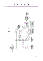
图1表示本发明的磁-光盘存贮器系统的第一实施方案;Fig. 1 shows the first embodiment of the magneto-optical storage system of the present invention;
图2表示一个首标区信息格式的例子;Fig. 2 shows an example of the information format of a header area;
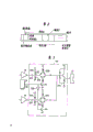
图3是首标部分和数据部分的开关电路布置图;Fig. 3 is a switch circuit layout diagram of a header part and a data part;
图4表示送至开关电路的输入信号和来自开关电路的输出信号及该开关电路的开关操作情况;Fig. 4 shows the input signal sent to the switching circuit and the output signal from the switching circuit and the switching operation of the switching circuit;
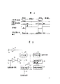
图5表示本发明的第二实施方案;Figure 5 represents a second embodiment of the present invention;
图6是一个时序图,表示根据图5的方案对信号进行开关和合成的操作情况;Fig. 6 is a sequence diagram showing the operation of switching and synthesizing signals according to the scheme of Fig. 5;
图7表示一个开关控制电路的例子;Figure 7 shows an example of a switch control circuit;
图8是一个时序图,表示图7的操作情况。FIG. 8 is a timing chart showing the operation of FIG. 7. FIG.
在磁-光盘之中,为了能在扇区单元中写入、读出或擦去数据,首标部分具有压刻凹点形式的控制信息。首标部分由下列内容构成:用于识别扇区初始位置的扇区标志,指示扇区地址的磁道号和扇区号,时钟同步信号,错误修正信号等等。另外,数据部分则安置在某个首标部分与另一首标部分之间。本发明因为分别包括了一个读首标检测系统和一个读数据检测系统,所以为了调节该两检测系统信号的电平并相应于每个部分选择来自任一检测系统的信号,需采用一定的措施。In magneto-optical discs, in order to enable data to be written, read or erased in sector units, the header portion has control information in the form of embossed pits. The header part is composed of the following contents: a sector mark used to identify the initial position of the sector, a track number and a sector number indicating the sector address, a clock synchronization signal, an error correction signal, and the like. Also, the data portion is placed between a certain header portion and another header portion. Because the present invention respectively includes a read header detection system and a read data detection system, so in order to adjust the level of the signals of the two detection systems and select the signal from any detection system corresponding to each part, certain measures need to be taken. .
在各个检测系统检测诸如相位信号和磁信号之类的各种不同信号,然后将其作为一系列信息项目处理的情况下,用某些方法对这两种信号进行开关操作及合成操作是必不可少的。为了控制开关操作,可考虑下述几种方法。In the case where various detection systems detect various signals such as phase signals and magnetic signals and then process them as a series of information items, it is necessary to switch and combine these two signals in some way Less. In order to control the switching operation, the following methods can be considered.
例如,为了进行旋转控制,盘面上形成了一些编码信号(凸凹图样),工作时对这些编码信号进行检测。当这些编码图形的数目和位置与盘上预备好的各个扇区相一致时,则可以根据编码信号的沿的时间识别首标部分与数据部分并运行一个开关电路,以便对这些来自互相分离的光检测器的检测信号进行开关和合成操作。但是该方法要求严格的条件,例如编码图形要与各个扇区位置精确相应,时序产生器电路要稳定工作而不允许受温度特性的影响等等。考虑到这些条件,该方法则不太适用了。For example, for rotation control, some coded signals (convex and concave patterns) are formed on the disk surface, and these coded signals are detected during operation. When the number and position of these coded patterns are consistent with each sector prepared on the disc, the header part and the data part can be identified according to the time of the edge of the coded signal and a switch circuit can be operated so that these data from separate Detection signals of the photodetectors are switched and synthesized. However, this method requires strict conditions, for example, the coding pattern should correspond to the position of each sector accurately, the timing generator circuit should work stably without being affected by temperature characteristics, and so on. Given these conditions, this approach is less applicable.
还可以考虑采用另一种措施,即:根据用于开关和合成的开关电路输出的信号来检测扇区标志,根据标志检测的时序对首标部分和数据部分进行开关操作。这种方法实际上是根据开关电路自身的信号的时序来进行开关操作。显然,当稳定地读出某些磁道时,这种开关操作可以是正常的。但是,当写入或擦掉状态中射在盘上的光量增加时,或进行从某磁道到另一磁道的存取时,则不能检测到扇区标志与首标信号。因此,当使用上述方法把变换开关掷到没有地址信息的数据一边时,便不能得到再把该变换开关掷回到首标部分一边的信号。所以,产生了一个缺陷,使下一步处理过程不能连续进行。It is also conceivable to adopt another measure, that is, to detect the sector mark according to the signal output by the switching circuit for switching and combining, and to switch the header part and the data part according to the timing of mark detection. This method actually performs the switching operation according to the timing of the signal of the switching circuit itself. Obviously, this switching operation may be normal when certain tracks are read stably. However, when the amount of light irradiated on the disk increases in the writing or erasing state, or when accessing from one track to another is performed, the sector mark and the header signal cannot be detected. Therefore, when the changeover switch is turned to the data side having no address information using the above method, a signal to turn the changeover switch back to the header portion side cannot be obtained. Therefore, a defect occurs so that the next processing cannot be continuously performed.
根据本发明,首标检测一边的光检测信号在进入变换开关之前被直接加到一个扇区标志检测电路上,而变换开关的工作是根据标志检测信号(该信号表示已检测到扇区标志)产生的时序运行的。因此,在对另外磁道的存取结束后,能够可靠地检测到扇区信号,这样便解决了上面提到的那个缺点。In accordance with the present invention, the optical detection signal on the header detection side is applied directly to a sector mark detection circuit before entering the changeover switch, and the changeover switch operates in response to the mark detection signal (which signal indicates that a sector mark has been detected) generated timing runs. Therefore, after the access to another track ends, the sector signal can be reliably detected, thus solving the above-mentioned disadvantage.
根据发明另一个实施方案,当开始进行存取操作时,强迫设置变换开关,使其能把光检测信号传到首标检测边,于是执行存取操作,当到达目的磁道时,重新根据首标部分或数据部分执行开关操作。在这种情况下,扇区信号在开关电路后面的一个装置中被测到,即使变换开关根据标志检测信号的时序进行操作,也可以连续进行正常的处理工作。According to another embodiment of the invention, when the access operation is started, the change switch is forced to be set so that the light detection signal can be passed to the header detection side, so that the access operation is performed, and when the destination track is reached, the header is re-selected according to the header detection signal. section or data section to perform switching operations. In this case, the sector signal is detected in a device behind the switch circuit, and even if the changeover switch is operated in accordance with the timing of the flag detection signal, normal processing can be continued.
下面将说明本发明的实施方案。图1表明了第1个实施方案。该图表示本发明的磁-光盘存贮器的设置,还表示了磁-光盘的磁-光头和信号检测、处理系统的一些部分。一个校准透镜2把来自激光二极管1的一束花转换成校准光束,一个三角棱镜3把该光束变换为一束截面为园形光强度分布的光。在通过一个光束分离器4之后,一个聚焦透镜5将该光束聚为一个小光点,照射在具有记录膜(垂直磁膜)的盘6上。一个电磁线圈7建立起一个磁场以便进行写和擦除。通过检测反射光的Kerr旋转来读出信息。来自盘6的反射光重新穿过聚焦透镜5,然后被光束分离器4反射。该反射光进而被一个光束分离器8反射并经由一个检偏镜9,通过一个透镜,检偏后的光被导至光检测器10,由它检测磁信息和首标信息。工厂制做盘时预先提供具有压刻凹点形式的首标信息,这是很便利的。理由是首标信息表示一些信息项目,如:用于识别各扇区初始位置的扇区标志,时钟信号,磁道号和扇区号,这些都是对数据译码时所需的;而且一般来说,用户不需要改换这些信息项目。Embodiments of the present invention will be described below. Figure 1 shows a first embodiment. This figure shows the arrangement of the magneto-optical disk memory of the present invention, and also shows the magneto-optical head of the magneto-optical disk and some parts of the signal detection and processing system. A collimating
光束分离器11把穿过光束分离器8的光分成两部分,一部分被导至光检测器12以进行自动聚焦控制,另一部分被导至光检测器13以进行跟踪控制。作为一个例子,光束分离器11反射的光通过一个散光光学系统(该系统由一个球面透镜和一个柱面透镜组成)并且部分地被一个刀口所隔离,于是它被导至光检测器口以检测聚焦误差,另一方面,穿过光束分离器11的光通过一个球面透镜被导至分成两段的光检测器13以检测跟踪误差。The beam splitter 11 divides the light passing through the beam splitter 8 into two parts, one part is guided to the
光检测器13收到的光信号是一个被从盘6的反射光量大小所调制的信号。也就是说,不仅光检测器10可以检测到盘6上的压刻凹点形式的首标信息,光检测器13也可检测到它们。光检测器13所接收的信号光尚未穿过偏光镜9,所以优点是它不易受到盘6延迟的影响和磁化分布引起的极化分布的影响。因此,最好是用光检测器13一边的信号去读首标信息。当然必须采用检测器10一边的信号读出磁信息,因为它可以检测到极化平面的旋转。The optical signal received by the
激光发射光学系统,磁信号检测系统,首标信号检测系统和电磁线圈构成一个磁-光头。通过一个步进电机或直线电机带动(图中未示),该磁电-光头可以沿径向移动到盘6的任何希望的位置。The laser emitting optical system, the magnetic signal detection system, the header signal detection system and the electromagnetic coil constitute a magneto-optical head. Driven by a stepping motor or a linear motor (not shown in the figure), the magneto-optical head can move radially to any desired position on the disc 6 .
下面将稍加说明首标信息的格式。图2是首标信息格式的一个例子。虽然在执行本发明结束时首标信息项目不一定总是像图2所示的那样的格式和顺序,但为了方便起见,在一个扇区的起始位置应当提供一个扇区标志。此外,首标信息的每个组成部分的位数可以按需要设置。The format of the header information will be explained a little below. Fig. 2 is an example of the header information format. Although the format and order of the header information items may not always be as shown in FIG. 2 at the end of carrying out the present invention, for convenience, a sector mark should be provided at the beginning of a sector. In addition, the number of bits of each component of header information can be set as desired.
下面将说明扇区标志检测电路系统(它形成了本发明的实质部分)和处理方法,该处理方法涉及了对送给检测电路系统的信号的分路以及在磁信息和首标信息之间进行开关操作和合成。The sector mark detection circuitry (which forms an essential part of the invention) and the processing method involved in the demultiplexing of the signal to the detection circuitry and the switching between the magnetic information and the header information will now be described. Switch manipulation and compositing.
在图1的电路中,放大器14将检测首标信号的光检测器13接收的信号放大到适当的电平,放大后的信号被分路后分别送到扇区标志检测电路15和可变增益放大器16以便将首标信号电平调整为磁信息信号的电平。当扇区标志检测电15已经识别到扇区标志时,时序发动器17产生出信号18,以便进行首标部分和数据部分之间的开关操作,时序发生器17的作用是确定数据部分的界限(从首标部分到下一扇区初始位置的区域)。另一方面,放大器19对磁信号检测光检测器10接收的磁电光信号(数据信号)进行放大然后将其送到用于对首标部分和数据部分进行开关操作的开关电路20。开关电路20根据开关信号18对信号进行开关操作,使来自光检测器13的信号作为首标部分通过。之后,限幅电路21处理开关电路20的输出,最终的数字信号送至下一级的处理系统之中。In the circuit of Fig. 1, the
上述的是本发明第一实施方案,下面将简要说明时序产生器电路17及开关电路20。由于扇区标志检测器15本身是已知电路,在此不需任何特殊的改变,所以将不作说明。The foregoing is the first embodiment of the present invention, and the
图3是开关电路20的一个例子。电容器201和202分别把首标信号一边的放大器16放大的信号和磁信号一边的放大器19放大的信号的直流成分隔掉。之后,电阻器203、204和205、206把这些信号转换为中心值大约在中点电势V/2左右的信号,这些信号分别送到二极管开关207和208。来自时序发生器电路17的开关信号18控制二极管开关的通与断。FIG. 3 is an example of the
当从时序发生器电路17来的信号18为低电平时,反相器209把高电平送到三极管开关210的基极以便开通该三极管开关,因此,二极管开关207被接通。同时,三极管开关211的基极为低电平,因此,二极管开关208被断开。这样,仅仅首标信号被送到下一级。反之,当时序发生器电路17来的信号18为高电平时,二极管开关207断开,208接通。所以,仅仅数据信号被送到下一级。二极管开关所选的信号通过缓冲电路212然后送入限幅器电路21。缓冲电路21用于降低开关电路20的输出阻抗并稳定地送出信号。虽然图中以例子的形式给出了一个射极跟随器电路,但它可以是具有相同功能的其它形式的电路。When the
图3中的时序产生器电路17接收所产生的扇区标志检测信号,并以一个计数器确定数据部分的界限,也就是说它计示固定的时钟数,从而对应首标信号产生低电平数字门信号,对应数据部分产生高电平数字门信号(以上为一个例子)。当然,反之,当对应首标部分输出高电平而对应数据部分输出低电平时,通过把开关电路20的操作及转仍可执行相同的功能。The
图4表示时序产生器电路17产生的开关信号18以及首标部分和数据部分信号之间的开关状况。Figure 4 shows the switching
虽然本实施例中的开关电路20包含了二极管开关207和208,它也可以由高速模拟开关构成。对于这种情况,开关操作需要的时间周期要考虑系统的数据传输速率而加以选择。例如,当传输速率是每秒几百K字节数量级时,开关速度要低于一百毫微秒,开关时间周期由试验确定,最后根据实际信号处理电路的证实来加以调整。Although the
下面将说明本发明的第二实施方案。图5以方框图形式表现了光检测器等装置的工作过程。图1中的光检测器10和13之前的设置仍适用于第二方案,故不再说明。Next, a second embodiment of the present invention will be described. Figure 5 shows the working process of devices such as photodetectors in the form of a block diagram. The arrangement before the
参照图5,放大器19对光检测器10接收的数据部分磁信息放大。另一方向,放大器14对光检测器13接收的首标部分相应信息放大,可变增益放大器16把该放大后的信号电平调整为磁信息的电平。开关电路20对这两个信号进行选择。一方面,开关电路20的输出被限幅电路21处理并数字化,另一方向,该输出还分送到扇区标志检测电路15。当首标部分内的扇区标志被检测到时,时序产生器电路17输出用于对首标部分和数据部分进行开关操作的门信号218。同时,一个上级控制器(控制单元)应当发出存取操作指令。因此,开关控制电路将使得来自光检测器13的信号在存取指令信号23发出到存取操作结束的期间内,通过开关电路20进入后级的限幅器21及扇区标志检测电路15而不出任何错误。当存取指令信号23停止时,开关控制电路22被复位,以便根据时序产生器电路17的门信号218重新运行开关电路20。在此将参照一个时序图,该图涉及第一实施方案内没有包括而在第二实施方案所加入的部分,即存取指令信号23、门信号218、开关信号24和开关电路20的输出/输出信号。Referring to FIG. 5 , the
图6表示与第二实施方案有关的操作时序。在图6中,当不出现存取指令时,信号23呈高电平。当存取指令信号23为高电平时,时序产生器电路17根据扇区标志检测信号25产生的时间发出门信号218,即对应于首标信号的低电平和对应于数据信号的高电平,从而执行正常的开关操作。现在考虑已经给出存取指令的情况。此时,开关指令信号23从高电平变为低电平。同时,开关信号24被强制降到低电平,而与门信号218的状态无关。因此,开关电路20应这样来选择,使得只有读光检测器一边的首标部分信号可以在所有时间内通过。在存取操作结束及存取指令信号23变为高电平后,当检测到第一个扇区标志时,存取之前的正常开关操作被重复执行。Fig. 6 shows an operation sequence related to the second embodiment. In FIG. 6, signal 23 is high when no access command is present. When the
图7表示开关控制电路22的一个例子。图中的数字30表示一个延迟电路,用一个计数器来实现。当接收到扇区标志检测信号25时,延迟电路30送出一个检测信号31,所延迟的时间间隔,正好达到首标信号之后的数据部分的起始位置。由于延迟了检测信号31,通过反相器32被送入触发器33的复位端(R端),触发器33的
Q输出端34保持在高电平。因此,在检测到扇区标志的情况下,与门电路35的一个输入端34为高电平,可使门信号218原样传送过去,作为开关信号24。An example of the
如果已经开始了存取操作,存取操作信号23变为低电平,通过反相器36,把高电平加到触发器33的触发输入端(T端)。在此,触发器33的D输入端和置位端(set)被拉到高电平(VoH)。因此,相应于T端的升高,触发器的
Q端变低。因此,即使门信号218为高电平,开关信号24也被强迫变为低电平,于是开关电路20使首标部分检测一边的信号通过。在存取操作结束后,当检测到扇区标志检测信号25时,开关电路恢复到相应于首标部分和数据部分的正常开关操作状态。虽然本实施例中的触发器33是D触发器,它也可以是不同类型的触发器。此外,是否插入反相32和36,这要考虑所用的触发器的操作情况。If the access operation has started, the
图8表示图7中的开关电路20相应于上面叙述的逻辑操作情况。FIG. 8 shows the operation of the
首标部分以压刻凹点形成出现在盘上,而数据部分是以磁化方向形式写入的,当在一个磁-光盘文件系统中处理这种类型的磁-光盘时(在该文件系统中分别设置了一个读首标部分的光检测器和一个读数据部分的光检测器),本发明的一个实施方案控制这样的时间,即在此时间上,来自两个检测器的信号根据来自读首标部分光检测器直接加入的信号进行开关和合成操作。这时,根据本发明,即使首标信号的读出操作被存取操作中断和系统复位时,开关操作也会立即重新开始。因此数据可以在扇区单元中稳定可靠地进行写入、读出和擦除。此外,根据本发明另一实施方案,开关时序取决于一个扇区标志,该标志从已经通过转换开关电路的信号中检测出来,但该变换开关被强迫设置,使来自首标部分读光检测器的信号仅在存取操作期间内无误地通过,并且在存取结束时,该变换开关被恢复成正常开关操作,从而实现一个同样的效果。The header portion appears on the disc in the form of embossed pits, while the data portion is written in the form of magnetization orientation. When dealing with this type of magneto-optical disc in a magneto-optical file system (in the A photodetector for reading the header part and a photodetector for reading the data part are respectively provided), and one embodiment of the present invention controls the time at which the signals from the two detectors are based on the signals from the read The signals directly added by the photodetectors of the header part are switched and synthesized. At this time, according to the present invention, even when the reading operation of the header signal is interrupted by the access operation and the system is reset, the switching operation is restarted immediately. Therefore, data can be written, read and erased stably and reliably in sector units. Furthermore, according to another embodiment of the present invention, the switching timing depends on a sector flag detected from a signal that has passed through the switch circuit, but the switch is forced to be set so that the read photodetector from the header portion The signal passes without error only during the access operation, and at the end of the access, the changeover switch is restored to normal switching operation, thereby achieving a same effect.
Claims (4)
Applications Claiming Priority (2)
| Application Number | Priority Date | Filing Date | Title |
|---|---|---|---|
| JP60008980A JPH07105081B2 (en) | 1985-01-23 | 1985-01-23 | Magneto-optical disk device and information processing method thereof |
| JP8980/85 | 1985-01-23 |
Publications (2)
| Publication Number | Publication Date |
|---|---|
| CN86100902A true CN86100902A (en) | 1986-08-20 |
| CN86100902B CN86100902B (en) | 1988-12-14 |
Family
ID=11707835
Family Applications (1)
| Application Number | Title | Priority Date | Filing Date |
|---|---|---|---|
| CN86100902A Expired CN86100902B (en) | 1985-01-23 | 1986-01-23 | magneto-optical storage system |
Country Status (6)
| Country | Link |
|---|---|
| US (1) | US4730289A (en) |
| EP (1) | EP0189187B1 (en) |
| JP (1) | JPH07105081B2 (en) |
| KR (1) | KR900000019B1 (en) |
| CN (1) | CN86100902B (en) |
| DE (1) | DE3666891D1 (en) |
Families Citing this family (31)
| Publication number | Priority date | Publication date | Assignee | Title |
|---|---|---|---|---|
| US5189651A (en) * | 1986-05-12 | 1993-02-23 | Pioneer Electronic Corporation | Optical system in magneto-optical recording and reproducing device |
| JP2574765B2 (en) * | 1986-07-09 | 1997-01-22 | 株式会社日立製作所 | Magneto-optical disk device |
| JP2779409B2 (en) * | 1986-08-26 | 1998-07-23 | キヤノン株式会社 | Electron beam irradiation position detecting device and information recording / reproducing device using the same |
| US4967403A (en) * | 1986-08-25 | 1990-10-30 | Sony Corporation | Multi-format optical disk and reading device |
| US5251196A (en) * | 1987-09-30 | 1993-10-05 | Deutsche Thomson-Brandt Gmbh | Optical pick-up selectively reading and writing an optical and magneto-optical recorded medium |
| GB8624444D0 (en) * | 1986-10-11 | 1986-11-12 | London Weekend Television Ltd | Optical disc |
| US4937800A (en) * | 1986-12-22 | 1990-06-26 | International Business Machines Corporation | Method of recording using selective-erasure directions for magnetooptic record members |
| US4916680A (en) * | 1986-12-22 | 1990-04-10 | International Business Machines Corporation | Magnetooptic recording member having selectively-reversed erasure directions in predetermined recording areas of the record member |
| US5051970A (en) * | 1987-05-08 | 1991-09-24 | Nippon Telegraph And Telephone Corporation | Magneto-optic recording system with overwrite capability |
| US5020040A (en) * | 1987-06-24 | 1991-05-28 | Digital Equipment Corporation | Overwriting system for magneto-optical recording with self timing track |
| US5043960A (en) * | 1987-09-25 | 1991-08-27 | Hitachi, Ltd. | Overwritable magneto-optic recording and reproducing apparatus |
| DE3732875A1 (en) * | 1987-09-30 | 1989-04-20 | Thomson Brandt Gmbh | OPTICAL RECORD CARRIER |
| US4931635A (en) * | 1987-12-01 | 1990-06-05 | Teijin Seiki Company Limited | Optical position sensor using Faraday effect element and magnetic scale |
| JP2647875B2 (en) * | 1987-12-25 | 1997-08-27 | 株式会社日立製作所 | Magneto-optical signal recording / reproducing method |
| US4931634A (en) * | 1987-12-28 | 1990-06-05 | Teijin Seiki Company Limited | Optical position sensor using Kerr effect and a magnetic scale |
| US5166913A (en) * | 1988-01-27 | 1992-11-24 | Nec Corporation | Optical disk device for record and reproduction of additional information besides reproducing of basic information |
| US5034934A (en) * | 1988-07-15 | 1991-07-23 | Pioneer Electronic Corp. | Opto-magnetic disk unit with improved dynamic range characteristics and opto-magnetic disk therefor |
| US5111442A (en) * | 1988-09-20 | 1992-05-05 | Sony Corporation | Recordable optical disc storage device with limited storage capacity, and recording apparatus therefor |
| JP2698784B2 (en) * | 1989-07-21 | 1998-01-19 | シャープ株式会社 | Information recording / reproducing device |
| JPH03171453A (en) * | 1989-11-29 | 1991-07-24 | Sony Corp | Magneto-optical signal reproducing method |
| US5050144A (en) * | 1989-12-11 | 1991-09-17 | International Business Machines Corporation | Recording intensity modulated signals and polarization-modulated optical signals in the same area of a storage member |
| US5272692A (en) * | 1989-12-11 | 1993-12-21 | International Business Machines Corporation | Data storage member having areas in which intensity-modulated signals are overlaid with magneto-optically recorded signals |
| US5245598A (en) * | 1990-06-27 | 1993-09-14 | Burroughs Alan C | Method and apparatus for seek operations in an optical recording system including holding a focus error signal at track crossings |
| JP2959588B2 (en) * | 1991-02-14 | 1999-10-06 | ソニー株式会社 | Magneto-optical disk and method of recording and reproducing sector management information thereof |
| DE69318517T2 (en) * | 1992-11-20 | 1998-11-26 | Philips Electronics N.V., Eindhoven | Magneto-optical reading / writing device |
| JP2698303B2 (en) * | 1992-12-07 | 1998-01-19 | 三洋電機株式会社 | Recordable disk and disk recording device |
| JP2738304B2 (en) * | 1994-08-03 | 1998-04-08 | 株式会社日立製作所 | Signal processing method and apparatus |
| US6118753A (en) * | 1996-08-13 | 2000-09-12 | Hewlett-Packard Company | Erasable digital video disk with reference clock track |
| US6118632A (en) * | 1997-02-12 | 2000-09-12 | International Business Machines Corporation | Magnetic disk stack having laser-bump identifiers on magnetic disks |
| JP2000182241A (en) * | 1998-12-16 | 2000-06-30 | Hitachi Ltd | Head amplifier and optical disk device using the same |
| JP4183868B2 (en) * | 1999-12-07 | 2008-11-19 | 富士通株式会社 | Optical storage device |
Family Cites Families (9)
| Publication number | Priority date | Publication date | Assignee | Title |
|---|---|---|---|---|
| US4001883A (en) * | 1974-03-07 | 1977-01-04 | Honeywell Information Systems, Inc. | High density data storage on magnetic disk |
| GB1554641A (en) * | 1975-08-11 | 1979-10-24 | Casio Computer Co Ltd | Data-recording device |
| JPS5841578B2 (en) * | 1978-10-04 | 1983-09-13 | 株式会社日立製作所 | Control method for rotating storage device |
| US4229808A (en) * | 1978-12-21 | 1980-10-21 | Ncr Corporation | Method for recording multiple data segments on a storage disc with eccentricity factor |
| US4367497A (en) * | 1981-01-02 | 1983-01-04 | Sperry Corporation | Digital data formatting system for high density magnetic recording |
| JPS57140086A (en) * | 1981-02-23 | 1982-08-30 | Hitachi Ltd | Recording and reproducing circuit for vtr |
| US4443870A (en) * | 1981-10-15 | 1984-04-17 | Burroughs Corporation | Optical memory system providing track following |
| US4535439A (en) * | 1981-12-01 | 1985-08-13 | Matsushita Electric Industrial Co., Ltd. | Optical having index mark and sector mark |
| JPS6085727U (en) * | 1983-11-18 | 1985-06-13 | 三洋電機株式会社 | information reading device |
-
1985
- 1985-01-23 JP JP60008980A patent/JPH07105081B2/en not_active Expired - Fee Related
- 1985-12-27 KR KR1019850009851A patent/KR900000019B1/en not_active Expired
-
1986
- 1986-01-14 US US06/818,684 patent/US4730289A/en not_active Expired - Lifetime
- 1986-01-22 DE DE8686100813T patent/DE3666891D1/en not_active Expired
- 1986-01-22 EP EP86100813A patent/EP0189187B1/en not_active Expired
- 1986-01-23 CN CN86100902A patent/CN86100902B/en not_active Expired
Also Published As
| Publication number | Publication date |
|---|---|
| EP0189187B1 (en) | 1989-11-08 |
| JPH07105081B2 (en) | 1995-11-13 |
| DE3666891D1 (en) | 1989-12-14 |
| EP0189187A3 (en) | 1988-03-30 |
| CN86100902B (en) | 1988-12-14 |
| KR900000019B1 (en) | 1990-01-18 |
| US4730289A (en) | 1988-03-08 |
| KR860006093A (en) | 1986-08-18 |
| JPS61170938A (en) | 1986-08-01 |
| EP0189187A2 (en) | 1986-07-30 |
Similar Documents
| Publication | Publication Date | Title |
|---|---|---|
| CN86100902A (en) | magneto-optical storage system | |
| US4712203A (en) | Method and apparatus for thermo magnetic recording/erasing information with preselected magnetic field switching | |
| EP0294490B1 (en) | Optical disc discriminating device | |
| US5134607A (en) | Optical memory system for generating a timing control signal for detecting a recorded region through a playback signal | |
| JPH01311440A (en) | Magneto-optical information recording and reproducing device | |
| US4879703A (en) | Magneto-optic memory apparatus with defect detection of recording medium during erasing operation | |
| EP0430811A2 (en) | Magneto-optical signal reproducing apparatus | |
| US4631706A (en) | System for preventing the overwriting of previously optically recorded data and for reading optically recorded data during writing | |
| US5684772A (en) | Magneto-optical disc recording and reproducing system with level clamping | |
| EP0427478A2 (en) | Disk recording and reproducing apparatus using two laser beams | |
| JPH11162038A (en) | Device and method for reading recorded information from magnetooptical recording medium | |
| JP3165216B2 (en) | Mark edge recording method and apparatus | |
| EP0587350B1 (en) | Optical disc apparatus and miserasing preventing circuit and method | |
| KR19980087103A (en) | Disk drive unit | |
| US5420835A (en) | Magneto-optic disk apparatus | |
| JP3287841B2 (en) | Data playback device and disc playback device | |
| JP3438258B2 (en) | Optical disk, optical disk reproducing device and optical disk recording device | |
| US4916680A (en) | Magnetooptic recording member having selectively-reversed erasure directions in predetermined recording areas of the record member | |
| EP0599387B1 (en) | Magneto-optical read/write device | |
| JP3086465B2 (en) | Signal playback method | |
| JP2501914B2 (en) | Information recording / reproducing device | |
| JP2738304B2 (en) | Signal processing method and apparatus | |
| JP2753073B2 (en) | Optical disk drive | |
| JP2002150632A (en) | Magneto-optical recording / reproducing device | |
| JPH08153349A (en) | Digital data recording method, digital data recording device, digital data recording / reproducing device |
Legal Events
| Date | Code | Title | Description |
|---|---|---|---|
| C06 | Publication | ||
| PB01 | Publication | ||
| CI01 | Publication of corrected invention patent application |
Correction item: Agency Correct: Patent Agency of China Council For The Promotion Of International Trade False: China Patent Agent Ltd. Number: 14 Page: 59 Volume: 2 |
|
| C10 | Entry into substantive examination | ||
| SE01 | Entry into force of request for substantive examination | ||
| C13 | Decision | ||
| GR02 | Examined patent application | ||
| C14 | Grant of patent or utility model | ||
| GR01 | Patent grant | ||
| ERR | Gazette correction |
Free format text: CORRECT FROM: CHINA PATENT AGENCY CO., LTD. TO: CHINA INTERNATIONAL TRADE PROMOTING COMMITTEE PATENT AGENCY DEPARTMENT |
|
| C17 | Cessation of patent right | ||
| CX01 | Expiry of patent term |