CN87106903A - Make the method on inclined-plane at the edge of semiconductor wafer - Google Patents
Make the method on inclined-plane at the edge of semiconductor wafer Download PDFInfo
- Publication number
- CN87106903A CN87106903A CN87106903.2A CN87106903A CN87106903A CN 87106903 A CN87106903 A CN 87106903A CN 87106903 A CN87106903 A CN 87106903A CN 87106903 A CN87106903 A CN 87106903A
- Authority
- CN
- China
- Prior art keywords
- wafer
- semiconductor wafer
- grinding wheel
- grinding
- molybdenum
- Prior art date
- Legal status (The legal status is an assumption and is not a legal conclusion. Google has not performed a legal analysis and makes no representation as to the accuracy of the status listed.)
- Pending
Links
Images
Classifications
-
- H—ELECTRICITY
- H10—SEMICONDUCTOR DEVICES; ELECTRIC SOLID-STATE DEVICES NOT OTHERWISE PROVIDED FOR
- H10P—GENERIC PROCESSES OR APPARATUS FOR THE MANUFACTURE OR TREATMENT OF DEVICES COVERED BY CLASS H10
- H10P90/00—Preparation of wafers not covered by a single main group of this subclass, e.g. wafer reinforcement
- H10P90/12—Preparing bulk and homogeneous wafers
- H10P90/128—Preparing bulk and homogeneous wafers by edge treatment, e.g. chamfering
-
- B—PERFORMING OPERATIONS; TRANSPORTING
- B24—GRINDING; POLISHING
- B24B—MACHINES, DEVICES, OR PROCESSES FOR GRINDING OR POLISHING; DRESSING OR CONDITIONING OF ABRADING SURFACES; FEEDING OF GRINDING, POLISHING, OR LAPPING AGENTS
- B24B9/00—Machines or devices designed for grinding edges or bevels on work or for removing burrs; Accessories therefor
- B24B9/02—Machines or devices designed for grinding edges or bevels on work or for removing burrs; Accessories therefor characterised by a special design with respect to properties of materials specific to articles to be ground
- B24B9/06—Machines or devices designed for grinding edges or bevels on work or for removing burrs; Accessories therefor characterised by a special design with respect to properties of materials specific to articles to be ground of non-metallic inorganic material, e.g. stone, ceramics, porcelain
- B24B9/065—Machines or devices designed for grinding edges or bevels on work or for removing burrs; Accessories therefor characterised by a special design with respect to properties of materials specific to articles to be ground of non-metallic inorganic material, e.g. stone, ceramics, porcelain of thin, brittle parts, e.g. semiconductors, wafers
Landscapes
- Engineering & Computer Science (AREA)
- Chemical & Material Sciences (AREA)
- Ceramic Engineering (AREA)
- Inorganic Chemistry (AREA)
- Mechanical Engineering (AREA)
- Mechanical Treatment Of Semiconductor (AREA)
- Grinding And Polishing Of Tertiary Curved Surfaces And Surfaces With Complex Shapes (AREA)
- Grinding Of Cylindrical And Plane Surfaces (AREA)
- Thyristors (AREA)
Abstract
一种用于让半导体圆片(1)的边缘成型为斜边的方法,这边缘由一个倾斜安放的砂轮圆盘磨削而成。处在由压紧机构(3,6)组成的压紧装置中的半导体圆片(1)的对中可借助于一与之成合金接触的钼质圆片(2)完成,钼质圆片紧贴着仿形圆盘(9)转动。
采用具有适当颗粒度和粘结剂的金刚石砂轮圆盘是特别有利的。
A method for bevelling the edge of a semiconductor wafer (1), which is ground by a grinding wheel disc placed at an angle. The centering of the semiconductor wafer (1) in the pressing device consisting of the pressing mechanism (3, 6) can be done by means of a molybdenum wafer (2) in alloy contact with it, the molybdenum wafer Cling to the profiling disc (9) to rotate.
It is particularly advantageous to use diamond wheel discs with suitable grit size and bond.
Description
The invention relates to the technical field of high-power semiconductor devices. It is specifically discussed a method of producing a bevel at the edge of a semiconductor wafer, in particular for medium and high voltage diodes.
It has long been known that for power semiconductor devices with high barrier layers, in particular for medium-and high-voltage alloy junction diodes, by providing the semiconductor wafer of its base component with appropriately inclined edges (so-called "positive bevel") the electric field strength at the surface is reduced and the dielectric breakdown characteristics determined by the bulk characteristics are approximately achieved.
The current technology allows such a beveled edge shape to be formed in a variety of ways. For example, it is proposed in DE-PS 1589421 to bevel a semiconductor wafer with an ultrasonic tool, such as an ultrasonic drill.
Another method described in US-PS 3, 262, 234 is to use sand blasting for shaping.
Finally, AS mentioned in DE-AS 1539101, the edge of the semiconductor component can be beveled by a sand blasting process or a grinding process, but this document does not give any details about the method which can be used in practice.
Among semiconductor processing methods, the ultrasonic drill method described above is a relatively old one and is replaced by a sand blast method, because this method often causes damage to crystal lattices of semiconductor wafers and breakage of edges.
However, the use of sandblasting in mass production has the following disadvantages:
1. tolerances in the blasting process are difficult to repeat.
2. The abrasive blasting equipment, and particularly the nozzles, are extremely abrasive and very expensive to maintain.
3. The processing time is proportional to the wafer thickness, and thus the throughput of a production line is strongly dependent on the thickness of the semiconductor wafer.
Despite the disadvantages mentioned above, sand blasting has hitherto been widely used, since there is no good, practically proven forming method.
The object of the invention is to provide a method for producing a bevelled edge shape which is simple and easy to implement, provides reproducible results and requires only relatively low technical conditions.
The object of the invention is achieved by pressing the semiconductor wafer against the pad, the wafer being rotatable, the edge of the wafer being ground by the front face of a rotating grinding wheel, the axis of rotation of the grinding wheel intersecting the axis of rotation of the pressed semiconductor wafer at a suitable angle.
The core of the invention is the grinding of the semiconductor wafer with a grinding wheel, the bevel edge being formed purely by machining, so that the completely defined geometry of the grinding apparatus is maintained.
In a preferred embodiment, the wafer is alloyed with a molybdenum sheet prior to compaction, and the semiconductor wafer and molybdenum sheet combination is then compacted and then ground. Thus, the mechanical load on the semiconductor wafer during polishing can be significantly reduced.
In a further preferred embodiment, a diamond grinding wheel is selected, having the specifications: the diamond particles had an average diameter of 25 microns and a density of about 3.3 carats/cm3Embedded in a metal binder. With such a grinding wheel a very uniform and precise bevel edge shape can be achieved, while at the same time having a sufficient life.
The invention is further elucidated below with the aid of the drawing in combination with an embodiment.
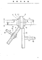
The only figure herein shows a geometric layout of a grinding apparatus that can be used to implement the machining method defined according to a preferred embodiment of the invention.
The drawing shows schematically a grinding device whereby the edges of a semiconductor wafer can be beveled.
For this purpose, the semiconductor wafer 1 is preferably first alloyed to the molybdenum wafer 2, and the molybdenum wafer can then be used as an alloy contact for the finished component.
The sheet-like structure composed of the semiconductor wafer 1 and the molybdenum wafer 2 is then pressed between two pressing devices 3 and 6 with corresponding clamping jaws 4 and 5. The pressing mechanisms 3 and 6 are rotatable, so that the semiconductor wafers to be pressed can also be rotated during grinding.
The pressing device consisting of the pressing mechanisms 3 and 6 has a rotating shaft, and the grinding wheel 7 is mounted on a grinding wheel shaft 8, which are suitably arranged at an angle to each other so that the desired bevel edge can be ground on the semiconductor wafer 1 with the front side of the grinding wheel. The angle of the bevel is thus determined by the angle between the axis of rotation of the pressing device and the axis of rotation 8 of the grinding wheel.
In order to obtain the same edge shape around the entire periphery of the semiconductor wafer, it is necessary to use a pressing device with a fixed axis of rotation. While the semiconductor wafer needs to be centered carefully during the pressing, if a pressing device is used which is movable perpendicular to the axis of rotation (as indicated by the double arrow in the figure), this time consuming and still error-free centering process can be avoided.
This allows the edge of the compacted molybdenum disc 2 to be in contact with a rotatable profiling disc 9, the axis of rotation 10 of which is fixed.
During the grinding process, when the molybdenum wafer 2 rolls along the profiling disk 9, the molybdenum wafer 2 and the semiconductor wafer are still rotated axially in a tangential manner with respect to the grinding wheel 7, even if the semiconductor wafer is not perfectly centered in the holding-down device. An inaccurate pairing during pressing will be represented by an oscillating movement of the pressing means 3 and 6 in the direction of the double arrow.
The grinding wheel 7 will move toward the semiconductor wafer 1 by the feed amount V during grinding (in the direction of the single arrow in the figure). For diamond grinding wheels, which will be described in more detail below, the feed V is preferably chosen to be 4 mm/min in order to reduce the machining time while at the same time obtaining a good surface structure.
For silicon diodes with a cut-off voltage of 300 to 6000 volts, the silicon thickness is 200 to 1000 microns, and diamond grinding wheels with the following specifications are preferably selected for batch production:
1. the diameter of the grinding wheel is about 150 mm.
2. The grinding wheel contained diamond particles having an average diameter of 25 microns.
3. The diamond grains had a density of about 3.3 carats/cm3(C75)。
4. Diamond particles are embedded in a metal binder in a grinding wheel.
Working with such a grinding wheel it is preferred to grind at a cutting speed of 22 meters per second, which has proven to be even more effective if the semiconductor wafer 1 is rotated against the grinding wheel 7 at a speed of 30 revolutions per minute during grinding.
Simple water is preferably used as the cooling liquid, and some rust inhibitor may be added to protect the grinding equipment.
In summary, the present invention provides a processing method, which can:
1. ensuring a very repeatable shape and tolerance of the bevel ("positive bevel").
2. The throughput of the apparatus is independent of the thickness of the semiconductor wafer.
3. The failure rate of the equipment is low, and the maintenance cost is low.
Drawing notes:
1. semiconductor wafer
2. Molybdenum disk
3.6 pressing mechanism
4.5. Chuck jaw
7. Grinding wheel
8. Grinding wheel spindle
9. Profiling disk
10. Profiling disc shaft
11. Edge of disc
V direction of feed
Claims (10)
Applications Claiming Priority (3)
| Application Number | Priority Date | Filing Date | Title |
|---|---|---|---|
| CH4070/86 | 1986-10-13 | ||
| CH4070/86A CH671116A5 (en) | 1986-10-13 | 1986-10-13 | |
| CH4070/86-0 | 1986-10-13 |
Publications (2)
| Publication Number | Publication Date |
|---|---|
| CN87106903A true CN87106903A (en) | 1988-04-20 |
| CN1005943B CN1005943B (en) | 1989-11-29 |
Family
ID=4269257
Family Applications (1)
| Application Number | Title | Priority Date | Filing Date |
|---|---|---|---|
| CN87106903.2A Expired CN1005943B (en) | 1986-10-13 | 1987-10-13 | Method for producing bevels on the edge of semiconductor wafer |
Country Status (6)
| Country | Link |
|---|---|
| US (1) | US4793102A (en) |
| EP (1) | EP0264679B1 (en) |
| JP (1) | JPS63102859A (en) |
| CN (1) | CN1005943B (en) |
| CH (1) | CH671116A5 (en) |
| DE (1) | DE3777528D1 (en) |
Cited By (2)
| Publication number | Priority date | Publication date | Assignee | Title |
|---|---|---|---|---|
| CN101851488A (en) * | 2009-03-31 | 2010-10-06 | 三河市科大博德粉末有限公司 | Ceramic bond diamond grinding block and manufacturing method thereof |
| CN104526493A (en) * | 2014-11-18 | 2015-04-22 | 天津中环领先材料技术有限公司 | Monocrystalline silicon wafer edge polishing technology |
Families Citing this family (9)
| Publication number | Priority date | Publication date | Assignee | Title |
|---|---|---|---|---|
| US5128281A (en) * | 1991-06-05 | 1992-07-07 | Texas Instruments Incorporated | Method for polishing semiconductor wafer edges |
| JPH0715897B2 (en) * | 1991-11-20 | 1995-02-22 | 株式会社エンヤシステム | Wafer end face etching method and apparatus |
| KR0185234B1 (en) * | 1991-11-28 | 1999-04-15 | 가부시키 가이샤 토쿄 세이미쯔 | Method of chamfering semiconductor wafer |
| US5595522A (en) * | 1994-01-04 | 1997-01-21 | Texas Instruments Incorporated | Semiconductor wafer edge polishing system and method |
| US5674110A (en) * | 1995-05-08 | 1997-10-07 | Onix S.R.L. | Machine and a process for sizing and squaring slabs of materials such as a glass, stone and marble, ceramic tile and the like |
| RU2163408C1 (en) * | 2000-02-08 | 2001-02-20 | Воронежская государственная технологическая академия | Chamfering device for finishing semiconductor plates |
| RU2168796C1 (en) * | 2000-07-10 | 2001-06-10 | Воронежская государственная технологическая академия | Gear to take off chamfer in process of finishing treatment of semiconductor plate |
| JP4852806B2 (en) * | 2000-07-27 | 2012-01-11 | 日立金属株式会社 | Chamfering method and apparatus for rare earth magnet |
| JP7549322B2 (en) * | 2020-04-01 | 2024-09-11 | 株式会社ノベルクリスタルテクノロジー | Semiconductor substrate and manufacturing method thereof |
Family Cites Families (13)
| Publication number | Priority date | Publication date | Assignee | Title |
|---|---|---|---|---|
| US2782565A (en) * | 1954-03-25 | 1957-02-26 | Landis Tool Co | Valve grinder |
| US3262234A (en) * | 1963-10-04 | 1966-07-26 | Int Rectifier Corp | Method of forming a semiconductor rim by sandblasting |
| GB1048740A (en) * | 1964-11-30 | 1966-11-16 | Westinghouse Brake & Signal | Semi-conductor elements |
| SU435926A1 (en) * | 1972-11-09 | 1974-07-15 | Н. В. Фокин | DEVICE FOR PROCESSING OF PROTECTIONS LENSES |
| US4031667A (en) * | 1976-03-29 | 1977-06-28 | Macronetics, Inc. | Apparatus for contouring edge of semiconductor wafers |
| DE2807268C3 (en) * | 1978-02-21 | 1981-02-12 | Prontor-Werk Alfred Gauthier Gmbh, 7547 Wildbad | Machine for centering optical lenses |
| US4227347A (en) * | 1978-09-14 | 1980-10-14 | Silicon Valley Group, Inc. | Two motor drive for a wafer processing machine |
| FR2437271A1 (en) * | 1978-09-26 | 1980-04-25 | Crouzet Sa | Silicon slice shaping machine - has rocker arms with rotary suction cups and self-centring grinding wheels |
| US4344260A (en) * | 1979-07-13 | 1982-08-17 | Nagano Electronics Industrial Co., Ltd. | Method for precision shaping of wafer materials |
| JPS5726439A (en) * | 1980-07-24 | 1982-02-12 | Nec Corp | Manufacture of semiconductor device |
| JPS58202758A (en) * | 1982-05-21 | 1983-11-26 | Hitachi Ltd | Grinding apparatus |
| US4580368A (en) * | 1982-11-30 | 1986-04-08 | Energy Adaptive Grinding, Inc. | Centerless and center-type grinding systems |
| JPS59224250A (en) * | 1983-06-03 | 1984-12-17 | Toshiba Corp | Grinding method |
-
1986
- 1986-10-13 CH CH4070/86A patent/CH671116A5/de not_active IP Right Cessation
-
1987
- 1987-10-01 DE DE8787114331T patent/DE3777528D1/en not_active Expired - Lifetime
- 1987-10-01 EP EP87114331A patent/EP0264679B1/en not_active Expired - Lifetime
- 1987-10-05 US US07/104,224 patent/US4793102A/en not_active Expired - Fee Related
- 1987-10-13 JP JP62258180A patent/JPS63102859A/en active Pending
- 1987-10-13 CN CN87106903.2A patent/CN1005943B/en not_active Expired
Cited By (2)
| Publication number | Priority date | Publication date | Assignee | Title |
|---|---|---|---|---|
| CN101851488A (en) * | 2009-03-31 | 2010-10-06 | 三河市科大博德粉末有限公司 | Ceramic bond diamond grinding block and manufacturing method thereof |
| CN104526493A (en) * | 2014-11-18 | 2015-04-22 | 天津中环领先材料技术有限公司 | Monocrystalline silicon wafer edge polishing technology |
Also Published As
| Publication number | Publication date |
|---|---|
| CH671116A5 (en) | 1989-07-31 |
| EP0264679B1 (en) | 1992-03-18 |
| EP0264679A1 (en) | 1988-04-27 |
| DE3777528D1 (en) | 1992-04-23 |
| JPS63102859A (en) | 1988-05-07 |
| US4793102A (en) | 1988-12-27 |
| CN1005943B (en) | 1989-11-29 |
Similar Documents
| Publication | Publication Date | Title |
|---|---|---|
| US4663890A (en) | Method for machining workpieces of brittle hard material into wafers | |
| CN103561908B (en) | Hard and brittle material grinding, grinding processing system and grinding, grinding method | |
| JP3534115B1 (en) | Edge-polished nitride semiconductor substrate, edge-polished GaN free-standing substrate, and edge processing method for nitride semiconductor substrate | |
| CN102350666B (en) | Diamond grinding wheel of elliptical working face and mutual wear forming and trimming method thereof | |
| GB2302830A (en) | Conditioning polishing pads | |
| CN87107167A (en) | Method for making annular groove on edge of semiconductor wafer of semiconductor power element | |
| JP7803688B2 (en) | Chamfer grinding method and chamfer grinding device | |
| CN87106903A (en) | Make the method on inclined-plane at the edge of semiconductor wafer | |
| WO2019146336A1 (en) | Seed crystal for 4h-sic single-crystal growth, and method for processing said seed crystal | |
| JP2004096112A (en) | Semiconductor wafer processing | |
| US20210086323A1 (en) | Polishing device | |
| CN1103511A (en) | Process for smoothing the edge of semiconductor wafers | |
| US6537139B2 (en) | Apparatus and method for ELID grinding a large-diameter workpiece to produce a mirror surface finish | |
| US5108561A (en) | Method of dressing, dressing system and dressing electrode for conductive grindstone | |
| CN1833815A (en) | Method for removing material from a semiconductor wafer | |
| JP3648239B2 (en) | Silicon wafer manufacturing method | |
| CN107900792B (en) | Cluster dynamic pressure magnetorheological polishing equipment and method | |
| JP2001007064A (en) | Grinding method of semiconductor wafer | |
| JP2534951B2 (en) | Truing material for cBN wheels | |
| JP3479848B2 (en) | Adjustment method of super abrasive wheel | |
| JPH0222219Y2 (en) | ||
| JP2003117800A (en) | Surface treatment method for polycrystalline Si ingot | |
| CN1394730A (en) | Production process of ceramic gauge block and its equipment | |
| JPH07164327A (en) | Cutting blade and electrolytic dressing, grinding and cutting device | |
| RU2108225C1 (en) | Method for cutting semiconducting ingots into plates |
Legal Events
| Date | Code | Title | Description |
|---|---|---|---|
| C10 | Entry into substantive examination | ||
| SE01 | Entry into force of request for substantive examination | ||
| C06 | Publication | ||
| PB01 | Publication | ||
| C13 | Decision | ||
| GR02 | Examined patent application | ||
| AD01 | Patent right deemed abandoned | ||
| C20 | Patent right or utility model deemed to be abandoned or is abandoned |