DE102019211971B4 - Semiconductor module - Google Patents
Semiconductor module Download PDFInfo
- Publication number
- DE102019211971B4 DE102019211971B4 DE102019211971.9A DE102019211971A DE102019211971B4 DE 102019211971 B4 DE102019211971 B4 DE 102019211971B4 DE 102019211971 A DE102019211971 A DE 102019211971A DE 102019211971 B4 DE102019211971 B4 DE 102019211971B4
- Authority
- DE
- Germany
- Prior art keywords
- semiconductor
- light
- voltage
- semiconductor module
- module according
- Prior art date
- Legal status (The legal status is an assumption and is not a legal conclusion. Google has not performed a legal analysis and makes no representation as to the accuracy of the status listed.)
- Active
Links
Images

Classifications
-
- H—ELECTRICITY
- H10—SEMICONDUCTOR DEVICES; ELECTRIC SOLID-STATE DEVICES NOT OTHERWISE PROVIDED FOR
- H10W—GENERIC PACKAGES, INTERCONNECTIONS, CONNECTORS OR OTHER CONSTRUCTIONAL DETAILS OF DEVICES COVERED BY CLASS H10
- H10W90/00—Package configurations
-
- H—ELECTRICITY
- H10—SEMICONDUCTOR DEVICES; ELECTRIC SOLID-STATE DEVICES NOT OTHERWISE PROVIDED FOR
- H10D—INORGANIC ELECTRIC SEMICONDUCTOR DEVICES
- H10D1/00—Resistors, capacitors or inductors
- H10D1/40—Resistors
- H10D1/47—Resistors having no potential barriers
-
- H—ELECTRICITY
- H10—SEMICONDUCTOR DEVICES; ELECTRIC SOLID-STATE DEVICES NOT OTHERWISE PROVIDED FOR
- H10D—INORGANIC ELECTRIC SEMICONDUCTOR DEVICES
- H10D1/00—Resistors, capacitors or inductors
- H10D1/60—Capacitors
- H10D1/68—Capacitors having no potential barriers
Landscapes
- Led Device Packages (AREA)
- Power Conversion In General (AREA)
- Engineering & Computer Science (AREA)
- Power Engineering (AREA)
- Inverter Devices (AREA)
- Semiconductor Integrated Circuits (AREA)
- Led Devices (AREA)
Abstract
Halbleitermodul, umfassend:ein Halbleitergehäuse (1), in welchem eine Halbleitervorrichtung (10, 11) eingebaut ist;eine Löschschaltung (13) mit einem Löschkondensator (4) und einem Löschwiderstand (5, 6), welche mit der Halbleitervorrichtung (10, 11) parallel verbunden sind;eine erste lichtemittierende Vorrichtung (7), die Licht emittiert, wenn eine Restspannung zwischen einer Anode und einer Kathode der Halbleitervorrichtung (10, 11) gleich einer ersten Spannung oder höher wird; undeine zweite lichtemittierende Vorrichtung (8), die Licht emittiert, wenn die Restspannung gleich einer zweiten Spannung oder höher wird,wobei die ersten und zweiten Spannungen voneinander verschieden sind.A semiconductor module comprising:a semiconductor package (1) in which a semiconductor device (10, 11) is installed;an erase circuit (13) having an erase capacitor (4) and an erase resistor (5, 6) connected in parallel to the semiconductor device (10, 11);a first light emitting device (7) that emits light when a residual voltage between an anode and a cathode of the semiconductor device (10, 11) becomes equal to a first voltage or higher; anda second light emitting device (8) that emits light when the residual voltage becomes equal to a second voltage or higher,the first and second voltages being different from each other.
Description
Hintergrund der ErfindungBackground of the invention
GebietArea
Die vorliegende Erfindung bezieht sich auf ein Halbleitermodul, das eine lichtemittierende Vorrichtung zum Emittieren von Licht entsprechend einer Restspannung enthält.The present invention relates to a semiconductor module including a light emitting device for emitting light according to a residual voltage.
Hintergrundbackground
Elektrizität nutzende Geräte arbeiten, indem eine Spannung angelegt wird, um einen Halbleiterschalter zu erregen. Wenn es notwendig ist, eine elektrische Schaltung zur Wartung, zum Austausch eines Halbleitermoduls oder dergleichen direkt zu adjustieren bzw. anzupassen, ist es aus Sicherheitsgründen wie etwa der Vermeidung eines Stromschlags wesentlich, das Vorhandensein oder Nichtvorhandensein einer Restspannung des Halbleitermoduls zu überprüfen. Herkömmlicherweise wurde das Vorhandensein oder Nichtvorhandensein der Restspannung über ein externes Messgerät wie etwa ein Oszilloskop überprüft. Wenn jedoch aufgrund eines Stromausfalls oder dergleichen die Stromversorgung unterbrochen ist und somit kein externes Messgerät verwendet werden kann, war es unmöglich, das Vorhandensein oder Nichtvorhandensein der Restspannung zu überprüfen. Auf der anderen Seite wurde eine Technik vorgeschlagen, die imstande ist, das Vorhandensein oder Nichtvorhandensein einer Restspannung basierend auf einer Lichtemission einer lichtemittierenden Vorrichtung, die mit einem Snubber- bzw. Löschkondensator parallel verbunden ist, zu überprüfen, wenn die Spannung des Löschkondensators nicht entladen wurde (zum Beispiel siehe
ZusammenfassungSummary
Im Stand der Technik war es jedoch nur möglich zu überprüfen, ob die Restspannung gleich einem vorbestimmten Wert oder geringer ist, und somit war es unmöglich, den Pegel der Restspannung zu überprüfen.However, in the prior art, it was only possible to check whether the residual voltage was equal to or less than a predetermined value, and thus it was impossible to check the level of the residual voltage.
Überdies wird im Stand der Technik die lichtemittierende Vorrichtung an einem Kondensator einer Hauptschaltung angebracht. Die lichtemittierende Vorrichtung wird jedoch nicht an jedes Halbleitergehäuse angebracht, in welchem eine Schaltvorrichtung und eine Diode eingebaut sind. Daher war es unmöglich, das Vorhandensein oder Nichtvorhandensein einer Restspannung in jedem Halbleitergehäuse zu überprüfen.Moreover, in the prior art, the light-emitting device is attached to a capacitor of a main circuit. However, the light-emitting device is not attached to each semiconductor package in which a switching device and a diode are incorporated. Therefore, it was impossible to check the presence or absence of a residual voltage in each semiconductor package.
Die
Die vorliegende Erfindung wurde gemacht, um die vorstehenden Probleme zu lösen, und hat eine erste Aufgabe, ein Halbleitermodul vorzusehen, das imstande ist, nicht nur das Vorhandensein oder Nichtvorhandensein einer Restspannung, sondern auch den Pegel der Restspannung zu überprüfen. Darüber hinaus hat die vorliegende Erfindung eine zweite Aufgabe, ein Halbleitermodul vorzusehen, das imstande ist, das Vorhandensein oder Nichtvorhandensein einer Restspannung für jedes Halbleitergehäuse zu überprüfen, in welchem eine Schaltvorrichtung und eine Diode eingebaut sind.The present invention has been made to solve the above problems, and has a first object to provide a semiconductor module capable of checking not only the presence or absence of a residual voltage but also the level of the residual voltage. Moreover, the present invention has a second object to provide a semiconductor module capable of checking the presence or absence of a residual voltage for each semiconductor package in which a switching device and a diode are installed.
Ein Halbleitermodul gemäß dem ersten Aspekt umfasst: ein Halbleitergehäuse, in welchem eine Halbleitervorrichtung eingebaut ist; eine Snubber- bzw. Löschschaltung mit einem Löschkondensator und einem Löschwiderstand, welche mit der Halbleitervorrichtung parallel verbunden sind; eine erste lichtemittierende Vorrichtung, die Licht emittiert, wenn eine Restspannung zwischen einer Anode und einer Kathode der Halbleitervorrichtung gleich einer ersten Spannung oder höher wird; und eine zweite lichtemittierende Vorrichtung, die Licht emittiert, wenn die Restspannung gleich einer zweiten Spannung oder höher wird, wobei die ersten und zweiten Spannungen voneinander verschieden sind.A semiconductor module according to the first aspect comprises: a semiconductor package in which a semiconductor device is installed; a snubber circuit having a snubber capacitor and a snubber resistor connected in parallel to the semiconductor device; a first light-emitting device that emits light when a residual voltage between an anode and a cathode of the semiconductor device becomes equal to a first voltage or higher; and a second light-emitting device that emits light when the residual voltage becomes equal to a second voltage or higher, the first and second voltages being different from each other.
Ein Halbleitermodul gemäß dem zweiten Aspekt umfasst: ein Halbleitergehäuse, in welchem eine Halbleitervorrichtung eingebaut ist; eine Löschschaltung mit einem Löschkondensator und einem Löschwiderstand, welche mit der Halbleitervorrichtung parallel verbunden sind; und eine lichtemittierende Vorrichtung, die aus dem Halbleitergehäuse freigelegt ist und Licht gemäß einer Restspannung zwischen einer Anode und einer Kathode der Halbleitervorrichtung emittiert, wobei die im Halbleitergehäuse eingebaute Halbleitervorrichtung nur eine Schaltvorrichtung und eine mit der Schaltvorrichtung antiparallel verbundene Diode enthält.A semiconductor module according to the second aspect comprises: a semiconductor package in which a semiconductor device is installed; an erase circuit having an erase capacitor and an erase resistor connected in parallel to the semiconductor device; and a light-emitting device exposed from the semiconductor package and emitting light according to a residual voltage between an anode and a cathode of the semiconductor device, wherein the semiconductor device installed in the semiconductor package has only one switching device and a diode connected anti-parallel to the switching device.
In dem ersten Aspekt sind zwei lichtemittierende Vorrichtungen mit verschiedenen Spannungswerten der Restspannung, die eine Lichtemission hervorruft, vorgesehen. Als Folge ist es möglich, nicht nur das Vorhandensein oder Nichtvorhandensein der Restspannung, sondern auch den Pegel der Restspannung zu überprüfen.In the first aspect, two light emitting devices having different voltage values of the residual voltage causing light emission are provided. As a result, it is possible to check not only the presence or absence of the residual voltage but also the level of the residual voltage.
In dem zweiten Aspekt wird die lichtemittierende Vorrichtung an jedes Halbleitergehäuse angebracht, in welchem eine Schaltvorrichtung und eine Diode eingebaut sind, und somit ist es möglich, das Vorhandensein oder Nichtvorhandensein einer Restspannung für jedes Halbleitergehäuse zu überprüfen.In the second aspect, the light emitting device is attached to each semiconductor package in which a switching device and a diode are installed, and thus it is possible to check the presence or absence of a residual voltage for each semiconductor package.
Andere und weitere Aufgaben, Merkmale und Vorteile der Erfindung werden aus der folgenden Beschreibung vollständiger ersichtlich werden.Other and further objects, features and advantages of the invention will become more fully apparent from the following description.
Kurze Beschreibung der ZeichnungenShort description of the drawings
-
1 ist eine Draufsicht, die ein Halbleitermodul gemäß einer ersten Ausführungsform zeigt.1 is a plan view showing a semiconductor module according to a first embodiment. -
2 ist eine Seitenansicht, die das Halbleitermodul gemäß der ersten Ausführungsform zeigt.2 is a side view showing the semiconductor module according to the first embodiment. -
3 ist ein Schaltungsdiagramm, das das Halbleitermodul gemäß der ersten Ausführungsform zeigt.3 is a circuit diagram showing the semiconductor module according to the first embodiment. -
4 zeigt eine Draufsicht, die ein Halbleitergehäuse darstellt, an dem ein Substrat nicht befestigt ist.4 shows a plan view illustrating a semiconductor package to which a substrate is not attached. -
5 ist eine Ansicht, die die Unterseite des Substrats darstellt.5 is a view showing the underside of the substrate. -
6 ist eine Seitenansicht, die ein Halbleitermodul gemäß einer zweiten Ausführungsform darstellt.6 is a side view illustrating a semiconductor module according to a second embodiment. -
7 ist eine Seitenansicht, die ein Halbleitermodul gemäß einer dritten Ausführungsform darstellt.7 is a side view illustrating a semiconductor module according to a third embodiment. -
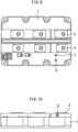
8 ist eine Seitenansicht, die ein Halbleitermodul gemäß einer vierten Ausführungsform darstellt.8th is a side view illustrating a semiconductor module according to a fourth embodiment. -
9 ist eine Draufsicht, die ein Halbleitermodul gemäß einer fünften Ausführungsform darstellt.9 is a plan view illustrating a semiconductor module according to a fifth embodiment. -
10 ist eine Seitenansicht, die das Halbleitermodul gemäß der fünften Ausführungsform darstellt.10 is a side view illustrating the semiconductor module according to the fifth embodiment. -
11 ist eine Draufsicht, die ein Halbleitermodul gemäß einer sechsten Ausführungsform darstellt.11 is a plan view illustrating a semiconductor module according to a sixth embodiment.
Beschreibung von AusführungsformenDescription of embodiments
Unter Bezugnahme auf die Zeichnungen wird ein Halbleitermodul gemäß den Ausführungsformen der vorliegenden Erfindung beschrieben. Die gleichen Komponenten werden durch die gleichen Symbole bezeichnet, und deren wiederholte Beschreibung kann weggelassen werden.A semiconductor module according to embodiments of the present invention will be described with reference to the drawings. The same components are denoted by the same symbols, and repeated descriptions thereof may be omitted.
Erste AusführungsformFirst embodiment
Der Löschkondensator 4 und die Löschwiderstände 5 und 6 sind mit der Schaltvorrichtung 10 und der Diode 11 parallel verbunden. Eine Löschschaltung 13 weist den Löschkondensator 4 und die Löschwiderstände 5, 6 auf. Der Löschwiderstand 5 hat einen Widerstandswert von etwa 150 kS2, und der Löschwiderstand 6 hat einen Widerstandswert von etwa 300 kΩ. Der Löschkondensator 4 hat einen Kapazitätswert auf dem nF-Niveau. Die erste lichtemittierende Vorrichtung 7 ist mit den Löschwiderständen 5 und 6 in Reihe verbunden. Die zweite lichtemittierende Vorrichtung 8 ist mit dem Löschwiderstand 5 in Reihe verbunden.The quenching capacitor 4 and the
Wenn zwischen der Anode und der Kathode der Schaltvorrichtung 10 eine Restspannung vorhanden ist, wird eine Spannung im Löschkondensator 4 geladen, und die ersten und zweiten lichtemittierenden Vorrichtungen 7 und 8 werden gemäß dem Spannungswert der geladenen Spannung erregt, um Licht zu emittieren. Die ersten und zweiten lichtemittierenden Vorrichtungen 7 und 8 emittieren Licht, wenn die Restspannung gleich einer ersten bzw. zweiten Spannung oder höher wird. Die ersten und zweiten Spannungen sind voneinander verschieden. Die erste lichtemittierende Vorrichtung 7 ist eine rote LED für eine hohe Spannung, und die zweite lichtemittierende Vorrichtung 8 ist eine blaue LED für eine Zwischenspannung.When a residual voltage exists between the anode and the cathode of the
Wenn die Restspannung eine hohe Spannung gleich der ersten Spannung oder höher ist, emittieren sowohl die erste als auch die zweite lichtemittierende Vorrichtung 7 und 8 Licht. Wenn die Restspannung eine Zwischenspannung ist, die gleich der zweiten Spannung oder höher und ebenfalls gleich der ersten Spannung oder niedriger ist, emittiert nur die zweite lichtemittierende Vorrichtung 8 Licht. Wenn die Restspannung niedriger als die zweite Spannung ist oder wenn keine Restspannung vorhanden ist, emittieren die beiden lichtemittierenden Vorrichtungen 7 und 8 kein Licht. Das Halbleitermodul gemäß der vorliegenden Ausführungsform weist eine Zustands-Anzeigefunktion auf, die imstande ist, diese drei Zustände basierend auf Lichtemissionsmustern der ersten und zweiten lichtemittierenden Vorrichtungen 7 und 8 zu überprüfen.When the residual voltage is a high voltage equal to or higher than the first voltage, both the first and second light-
Die erste Spannung wird in Anbetracht des oberen Grenzpegels von Schaltspannungen aktueller Halbleitermodule in einem Bereich von nicht weniger als 1000 V bis weniger als 4500 V eingestellt. Die zweite Spannung wird in einem Bereich von nicht weniger als 100 V bis weniger als 1000 V eingestellt. Wenn der Spannungswert der Restspannung eine niedrige Spannung geringer als 100 V ist, ist es unwahrscheinlich, dass die im Löschkondensator geladene Spannung ein Problem hervorruft, und somit ist es unnötig, den Pegel der Restspannung genau zu überprüfen.The first voltage is set in a range of not less than 1000 V to less than 4500 V in consideration of the upper limit level of switching voltages of current semiconductor modules. The second voltage is set in a range of not less than 100 V to less than 1000 V. If the voltage value of the residual voltage is a low voltage less than 100 V, the voltage charged in the quenching capacitor is unlikely to cause a problem, and thus it is unnecessary to check the level of the residual voltage precisely.
Wie oben beschrieben wurde, sind in der vorliegenden Ausführungsform zwei lichtemittierende Vorrichtungen mit unterschiedlichen Spannungswerten der Restspannung, die eine Lichtemission hervorruft, vorgesehen. Als Folge ist es möglich, nicht nur das Vorhandensein oder Nichtvorhandensein der Restspannung, sondern auch den Pegel der Restspannung zu überprüfen.As described above, in the present embodiment, two light emitting devices having different voltage values of the residual voltage causing light emission are provided. As a result, it is possible to check not only the presence or absence of the residual voltage but also the level of the residual voltage.
Zweite AusführungsformSecond embodiment
Dritte AusführungsformThird embodiment
Vierte AusführungsformFourth embodiment
Fünfte AusführungsformFifth embodiment
Sechste AusführungsformSixth embodiment
Die Schaltvorrichtung 10 und die Diode 11 sind nicht auf aus Silizium bestehende Halbleitervorrichtungen beschränkt, sondern können stattdessen aus einem Halbleiter mit breiter Bandlücke bestehen, der eine breitere Bandlücke als diejenige von Silizium aufweist. Der Halbleiter mit breiter Bandlücke ist beispielsweise ein Siliziumcarbid, ein Material auf Galliumnitrid-Basis oder Diamant. Eine Halbleitervorrichtung, die aus solch einem Halbleiter mit breiter Bandlücke besteht, weist eine hohe Spannungsfestigkeit und eine hohe zulässige Stromdichte auf und kann folglich miniaturisiert werden. Die Verwendung solch einer miniaturisierten Halbleitervorrichtung ermöglicht die Miniaturisierung und hohe Integration des Halbleitermoduls, in welchem die Halbleitervorrichtung eingebaut ist. Da die Halbleitervorrichtung eine hohe Wärmebeständigkeit aufweist, kann ferner eine Abstrahllamelle eines Kühlkörpers miniaturisiert werden, und ein wassergekühlter Teil kann luftgekühlt werden, was zu einer weiteren Miniaturisierung des Halbleitermoduls führt. Da die Halbleitervorrichtung ferner einen niedrigen Leistungsverlust und eine hohe Effizienz aufweist, kann ein hocheffizientes Halbleitermodul erreicht werden. Sowohl die Schaltvorrichtung 10 als auch die Diode 11 bestehen wünschenswerterweise aus einem Halbleiter mit breiter Bandlücke. Jedoch kann nur eine von ihnen aus einem Halbleiter mit breiter Bandlücke bestehen. Somit ist es möglich, die in dieser Ausführungsform beschriebenen Effekte zu erzielen.The switching
Claims (8)
Applications Claiming Priority (2)
| Application Number | Priority Date | Filing Date | Title |
|---|---|---|---|
| JP2018-157719 | 2018-08-24 | ||
| JP2018157719A JP6939740B2 (en) | 2018-08-24 | 2018-08-24 | Semiconductor module |
Publications (2)
| Publication Number | Publication Date |
|---|---|
| DE102019211971A1 DE102019211971A1 (en) | 2020-02-27 |
| DE102019211971B4 true DE102019211971B4 (en) | 2024-06-06 |
Family
ID=69412448
Family Applications (1)
| Application Number | Title | Priority Date | Filing Date |
|---|---|---|---|
| DE102019211971.9A Active DE102019211971B4 (en) | 2018-08-24 | 2019-08-09 | Semiconductor module |
Country Status (4)
| Country | Link |
|---|---|
| US (1) | US10818648B2 (en) |
| JP (1) | JP6939740B2 (en) |
| CN (1) | CN110858585B (en) |
| DE (1) | DE102019211971B4 (en) |
Families Citing this family (3)
| Publication number | Priority date | Publication date | Assignee | Title |
|---|---|---|---|---|
| DE112018007125T5 (en) * | 2018-02-20 | 2020-11-05 | Mitsubishi Electric Corporation | POWER SEMI-CONDUCTOR MODULE AND POWER CONVERTER WITH THE SAME |
| EP3761492B1 (en) * | 2019-07-05 | 2023-01-04 | Infineon Technologies AG | Snubber circuit and power semiconductor module with snubber circuit |
| JP7697253B2 (en) * | 2021-04-14 | 2025-06-24 | 富士フイルムビジネスイノベーション株式会社 | Light emitting device and measuring device |
Citations (2)
| Publication number | Priority date | Publication date | Assignee | Title |
|---|---|---|---|---|
| JP2013110821A (en) | 2011-11-18 | 2013-06-06 | Hitachi Automotive Systems Ltd | Power converter |
| JP2013179747A (en) | 2012-02-28 | 2013-09-09 | Denso Corp | Snubber circuit, power supply device including the same, and power supply device mounting vehicle |
Family Cites Families (15)
| Publication number | Priority date | Publication date | Assignee | Title |
|---|---|---|---|---|
| JPS5656657U (en) * | 1979-10-04 | 1981-05-16 | ||
| JPH0274162A (en) * | 1988-09-08 | 1990-03-14 | Toshiba Corp | Power converter |
| JPH0417562A (en) * | 1990-05-10 | 1992-01-22 | Toshiba Corp | Method of protecting thyristor converter |
| JPH0741473U (en) * | 1993-12-27 | 1995-07-21 | 財団法人関東電気保安協会 | Discharge rod with discharge level display function |
| JP3507911B2 (en) * | 1996-07-19 | 2004-03-15 | 株式会社日立製作所 | Power converter snubber circuit |
| JPH1169775A (en) * | 1997-08-06 | 1999-03-09 | Nissin Electric Co Ltd | Gto snubber voltage detection and detection circuit |
| JP4195398B2 (en) * | 2004-01-29 | 2008-12-10 | 関西電力株式会社 | Semiconductor device and power device using the same |
| JP2005354545A (en) * | 2004-06-14 | 2005-12-22 | Agilent Technol Inc | Socket |
| JP4882357B2 (en) | 2005-12-02 | 2012-02-22 | 富士電機株式会社 | Semiconductor device drive circuit |
| JP2008039741A (en) * | 2006-08-10 | 2008-02-21 | Chuden Kogyo Kk | Single-phase two-wire type surge suppression system |
| KR20090021811A (en) * | 2007-08-28 | 2009-03-04 | 삼성전자주식회사 | Semiconductor Module Mount Test Device |
| JP5244653B2 (en) * | 2009-03-03 | 2013-07-24 | 日立オートモティブシステムズ株式会社 | Power converter |
| JP6227480B2 (en) * | 2014-05-23 | 2017-11-08 | 三菱電機株式会社 | Semiconductor device |
| CN204065222U (en) * | 2014-08-07 | 2014-12-31 | 成都熊谷加世电器有限公司 | Electrochemical capacitor residual voltage indicating device |
| US20190207380A1 (en) * | 2018-01-02 | 2019-07-04 | Kenneth Matthew Michaels | Rejection of Capacitive Coupling with RDC Snubber circuit and LED indicators |
-
2018
- 2018-08-24 JP JP2018157719A patent/JP6939740B2/en active Active
-
2019
- 2019-05-07 US US16/405,019 patent/US10818648B2/en active Active
- 2019-08-09 DE DE102019211971.9A patent/DE102019211971B4/en active Active
- 2019-08-19 CN CN201910762832.XA patent/CN110858585B/en active Active
Patent Citations (3)
| Publication number | Priority date | Publication date | Assignee | Title |
|---|---|---|---|---|
| JP2013110821A (en) | 2011-11-18 | 2013-06-06 | Hitachi Automotive Systems Ltd | Power converter |
| US20140239870A1 (en) | 2011-11-18 | 2014-08-28 | Hitachi Automotive Systems, Ltd. | Power Conversion Apparatus |
| JP2013179747A (en) | 2012-02-28 | 2013-09-09 | Denso Corp | Snubber circuit, power supply device including the same, and power supply device mounting vehicle |
Also Published As
| Publication number | Publication date |
|---|---|
| US20200066697A1 (en) | 2020-02-27 |
| JP2020031526A (en) | 2020-02-27 |
| DE102019211971A1 (en) | 2020-02-27 |
| JP6939740B2 (en) | 2021-09-22 |
| CN110858585A (en) | 2020-03-03 |
| US10818648B2 (en) | 2020-10-27 |
| CN110858585B (en) | 2024-04-16 |
Similar Documents
| Publication | Publication Date | Title |
|---|---|---|
| DE102019211971B4 (en) | Semiconductor module | |
| WO2003075423A1 (en) | Diode laser array comprising a plurality of electrically series- connected diode lasers | |
| DE19919944A1 (en) | Arrangement with light emitting diodes with integrated protection against electrostatic discharge | |
| DE19600807A1 (en) | Intelligent, separated, half-bridge power module, e.g. inverter | |
| DE112019006063T5 (en) | SEMICONDUCTOR LASER COMPONENTS | |
| DE102020133680A1 (en) | Semiconductor device and method of manufacturing a semiconductor device | |
| DE102012105630B4 (en) | Lighting arrangement with lighting device and method for operating a lighting device | |
| DE102016103087A1 (en) | Module with light-emitting solid-state element and illumination arrangement | |
| DE102014205441A1 (en) | Backlight module and method for detecting its electrostatic damage | |
| AT396536B (en) | PROTECTIVE CIRCUIT FOR A INVERTER CIRCUIT FOR THE OPERATION OF GAS DISCHARGE LAMPS | |
| DE102014115226A1 (en) | ESD protection circuit | |
| DE3137079A1 (en) | SUPPLY DEVICE FOR A CURRENT MONITORING LIGHT INDICATOR | |
| DE112021004775T5 (en) | discharge circuit module | |
| WO2008000209A1 (en) | Illumination device | |
| DE3311426A1 (en) | Overvoltage protection device for an electrical valve, having feedback of a protective triggering in the event of overvoltage | |
| DE202015102462U1 (en) | Overvoltage and polarity reversal protection for LED modules in the vehicle | |
| DE102010060437B4 (en) | Device for operating a lighting module with overvoltage protection | |
| DE1538376B2 (en) | CIRCUIT ARRANGEMENT FOR THE PROTECTION OF A CONSUMER | |
| DE3707973C2 (en) | ||
| DE3134647C2 (en) | Overvoltage-limited control of light-ignited power semiconductors | |
| DE112016006919B4 (en) | Semiconductor device, ignition device for internal combustion engine and internal combustion engine system | |
| DE102022101272A1 (en) | light emitting module | |
| DE112020003807T5 (en) | SEMICONDUCTOR DEVICE | |
| DE9218434U1 (en) | Lighting device | |
| DE3878945T2 (en) | DEVICE FOR SUPPLYING ELECTRICAL ENERGY FOR A CABLE AND ITS APPLICATION. |
Legal Events
| Date | Code | Title | Description |
|---|---|---|---|
| R012 | Request for examination validly filed | ||
| R084 | Declaration of willingness to licence | ||
| R016 | Response to examination communication | ||
| R018 | Grant decision by examination section/examining division | ||
| R020 | Patent grant now final | ||
| R079 | Amendment of ipc main class |
Free format text: PREVIOUS MAIN CLASS: H01L0025160000 Ipc: H10W0090000000 |