DE10232425B4 - Semiconductor element - Google Patents
Semiconductor element Download PDFInfo
- Publication number
- DE10232425B4 DE10232425B4 DE10232425A DE10232425A DE10232425B4 DE 10232425 B4 DE10232425 B4 DE 10232425B4 DE 10232425 A DE10232425 A DE 10232425A DE 10232425 A DE10232425 A DE 10232425A DE 10232425 B4 DE10232425 B4 DE 10232425B4
- Authority
- DE
- Germany
- Prior art keywords
- layer
- semiconductor layer
- schottky metal
- main surface
- junction
- Prior art date
- Legal status (The legal status is an assumption and is not a legal conclusion. Google has not performed a legal analysis and makes no representation as to the accuracy of the status listed.)
- Expired - Fee Related
Links
Classifications
-
- H—ELECTRICITY
- H10—SEMICONDUCTOR DEVICES; ELECTRIC SOLID-STATE DEVICES NOT OTHERWISE PROVIDED FOR
- H10D—INORGANIC ELECTRIC SEMICONDUCTOR DEVICES
- H10D8/00—Diodes
- H10D8/80—PNPN diodes, e.g. Shockley diodes or break-over diodes
-
- H—ELECTRICITY
- H10—SEMICONDUCTOR DEVICES; ELECTRIC SOLID-STATE DEVICES NOT OTHERWISE PROVIDED FOR
- H10D—INORGANIC ELECTRIC SEMICONDUCTOR DEVICES
- H10D62/00—Semiconductor bodies, or regions thereof, of devices having potential barriers
- H10D62/10—Shapes, relative sizes or dispositions of the regions of the semiconductor bodies; Shapes of the semiconductor bodies
- H10D62/102—Constructional design considerations for preventing surface leakage or controlling electric field concentration
- H10D62/103—Constructional design considerations for preventing surface leakage or controlling electric field concentration for increasing or controlling the breakdown voltage of reverse-biased devices
- H10D62/105—Constructional design considerations for preventing surface leakage or controlling electric field concentration for increasing or controlling the breakdown voltage of reverse-biased devices by having particular doping profiles, shapes or arrangements of PN junctions; by having supplementary regions, e.g. junction termination extension [JTE]
- H10D62/106—Constructional design considerations for preventing surface leakage or controlling electric field concentration for increasing or controlling the breakdown voltage of reverse-biased devices by having particular doping profiles, shapes or arrangements of PN junctions; by having supplementary regions, e.g. junction termination extension [JTE] having supplementary regions doped oppositely to or in rectifying contact with regions of the semiconductor bodies, e.g. guard rings with PN or Schottky junctions
-
- H—ELECTRICITY
- H10—SEMICONDUCTOR DEVICES; ELECTRIC SOLID-STATE DEVICES NOT OTHERWISE PROVIDED FOR
- H10D—INORGANIC ELECTRIC SEMICONDUCTOR DEVICES
- H10D8/00—Diodes
-
- H—ELECTRICITY
- H10—SEMICONDUCTOR DEVICES; ELECTRIC SOLID-STATE DEVICES NOT OTHERWISE PROVIDED FOR
- H10D—INORGANIC ELECTRIC SEMICONDUCTOR DEVICES
- H10D84/00—Integrated devices formed in or on semiconductor substrates that comprise only semiconducting layers, e.g. on Si wafers or on GaAs-on-Si wafers
- H10D84/80—Integrated devices formed in or on semiconductor substrates that comprise only semiconducting layers, e.g. on Si wafers or on GaAs-on-Si wafers characterised by the integration of at least one component covered by groups H10D12/00 or H10D30/00, e.g. integration of IGFETs
- H10D84/86—Integrated devices formed in or on semiconductor substrates that comprise only semiconducting layers, e.g. on Si wafers or on GaAs-on-Si wafers characterised by the integration of at least one component covered by groups H10D12/00 or H10D30/00, e.g. integration of IGFETs of Schottky-barrier gate FETs
Landscapes
- Electrodes Of Semiconductors (AREA)
Abstract
Halbleiterelement
enthaltend:
eine zu Grunde liegende Halbleiterschicht mit einem
Gebiet, in welchem ein pn-Übergang
ausgebildet wird, wobei ein Ende des pn-Übergangs eine Hauptoberfläche der
zu Grunde liegenden Halbleiterschicht erreicht; und
mindestens
eine Schottky-Metallschicht (106), die wie ein Ring um die Hauptoberfläche der
zu Grunde liegenden Halbleiterschicht in einem Schottky-Kontakt
mit der zu Grunde liegenden Halbleiterschicht ausgeführt ist,
und um dieses Gebiet einzuschließen,
dadurch gekennzeichnet,
dass
die mindestens eine Schottky-Metallschicht (106) mit der Halbleiterschicht
zur Ausbildung einer Verarmungsregion (108) in Kontakt tritt, wobei
die Verarmungsregion (108) eine Tiefe aufweist, die gleich oder
größer einer
Tiefe eines Hauptübergangs
des pn-Übergangs
in der Hauptoberfläche
ist.Semiconductor element comprising:
an underlying semiconductor layer having a region in which a pn junction is formed, wherein an end of the pn junction reaches a main surface of the underlying semiconductor layer; and
at least one Schottky metal layer (106) formed around the main surface of the underlying semiconductor layer in a Schottky contact with the underlying semiconductor layer like a ring, and to enclose this region,
characterized in that
the at least one Schottky metal layer (106) contacts the semiconductor layer to form a depletion region (108), the depletion region (108) having a depth equal to or greater than a depth of a major junction of the pn junction in the major surface.
Description
Die Erfindung betrifft ein Halbleiterelement, insbesondere ein Halbleiterelement, das eine hohe Durchbruchspannung erfordert.The The invention relates to a semiconductor element, in particular a semiconductor element, which requires a high breakdown voltage.
Beschreibung eines herkömmlichen Ausführungsbeispiels nach dem Stand der Technik.description a conventional one embodiment According to the state of the art.
Es ist wichtig, dass ein Halbleiterelement, das eine hohe Spannung mittels eines pn-Übergangs absperrt, eine elektrische Feldstärke an einer Übergangsoberfläche, die sich in Kontakt mit einer Substanz, die eine verschiedene Dielektrizitätskonstante aufweist, unterstützen, und damit eine Durchbruchspannung in vergleichbarer Höhe mit einer Feldstärke im Übergang innerhalb des Siliziumsubstrates realisieren muss.It It is important that a semiconductor element that has a high voltage shut off by means of a pn junction, an electric field strength at a transitional surface, the in contact with a substance having a different dielectric constant, support, and thus a breakdown voltage at a comparable level with a field strength in transition must realize within the silicon substrate.
Aus diesem Grund wird eine Feldbegrenzungsringstruktur, eine SIPOS (Semi-Insulating Polycrystalline Silicon) Struktur und eine vergleichbare Struktur üblicherweise als eine Übergangsbeendigungsprozessstruktur verwendet.Out For this reason, a field limiting ring structure, a SIPOS (Semi-Insulating Polycrystalline Silicon) structure and a comparable structure usually as a transition completion process structure used.
SIPOS StrukturSIPOS structure
Wie
in
Eine
maximale Tiefe der p-Typ-Dotierungsschicht
Eine
Anodenelektrode
Der
SIPOS Film
Eine
n-Typ Dotierungsschicht
In
dem Fall, in welchem eine Rückspannung an
die Siliziumdiode
Weiterhin
fungiert der Siliziumnitritfilm
Im
folgenden wird eine Methode zum Aufbau der p-Typ Dotierungsschicht
Die
Fotolackmaske RM besitzt solch eine Schablonenform, dass eine Öffnung OP1
ein großes Gebiet,
welches einem Gebiet der tiefsten Diffusionsschicht in der dreistufigen
p-Typ Dotierungsschicht
Bei
Verwendung einer Photolackmaske RM, die solch eine Struktur aufweist,
als eine Ionenimplantationsmaske kann eine effektive Implantationsmenge
für jede
Diffusionsschicht geändert
werden und die p-Typ-Dotierungsschicht
FeldbegrenzungsringstrukturField limiting ring structure
Im
folgenden wird eine Schnittstruktur einer Siliziumcarbiddiode
Weil Siliziumcarbid eine größere Energielücke zwischen Bändern als diejenige von Silizium aufweist, weist dieses eine größere thermische Stabilität auf, sodass ein Siliziumcarbidelement bei einer hohen Temperatur von 1000 K (Kelvin) oder weniger betrieben werden kann. Zusätzlich dazu weist Siliziumcarbid eine hohe thermische Leitfähigkeit auf. Damit kann ein Siliziumcarbidelement bei einer hohen Dichte bereitgestellt werden.Because Silicon carbide has a larger energy gap between bands As that of silicon, this has a larger thermal Stability up, a silicon carbide element at a high temperature of 1000 K (Kelvin) or less can be operated. Additionally For example, silicon carbide has a high thermal conductivity. This can be a Silicon carbide element are provided at a high density.
Weiterhin weist Siliziumcarbid eine Durchbruchsfeldstärke auf, welche annähernd zehn mal größer als die von Silizium ist. In einem Störzustand ist daher Siliziumcarbid für ein Gerät verwendbar, das unter einer Bedingung betrieben wird, dass möglicherweise eine hohe Spannung erzeugt wird.Farther For example, silicon carbide has a breakdown field strength that is approximately ten sometimes bigger than which is of silicon. In a fault state is therefore silicon carbide for a Device usable, that is operated under a condition that may have a high voltage is produced.
Andererseits weist die SIPOS-Struktur eine hohe Temperaturabhängigkeit auf. In der Siliziumcarbiddiode, die einen großen Arbeitstemperaturbereich umfasst, besteht daher die Möglichkeit, dass sich ein Spannungssperrvermögen bei niedrigen und hohen Temperaturen extrem ändert. Deswegen, ist es nicht vorteilhaft, die SIPOS Struktur auf eine Siliziumcarbiddiode anzuwenden. Aus diesem Grund wird die Feldbegrenzungsringstruktur im allgemeinen an einer Siliziumcarbiddiode angewandt.on the other hand the SIPOS structure has a high temperature dependence. In the silicon carbide diode, the one big Operating temperature range, it is therefore possible to that is a voltage blocking capability Extreme changes at low and high temperatures. That's why, it's not beneficial apply the SIPOS structure to a silicon carbide diode. Out For this reason, the field boundary ring structure becomes general applied to a silicon carbide diode.
Wie
in
Die
epitaktische n-Typ Schicht
Eine
Seitenoberfläche
des Vorsprungs PP ist so ausgeführt,
dass eine Seitenoberfläche
der epitaktischen n-Typ Schicht
Ein
Siliziumoxidfilm
Darüber hinaus
ist der untere Basisabsatzteil BP selektiv mit einer p-Typ Dotierungsschicht
Eine
Anodenelektrode
Weil
der Feldbegrenzungsring
Ein
Verfahren zum Herstellen einer der Siliziumcarbiddiode
Bei
einem in
An
einem in gezeigten
In
einem in
Der
Vorsprung PP hat eine Schrägstruktur,
in welcher eine Seitenoberfläche
von dieser mit einem Neigungswinkel ausgebildet ist und eine Seitenoberfläche der
epitaktischen n-Typ Schicht
In
einem in
Nachdem
die Widerstandsfotolackmaske RM1 entfernt wurde, wird ein Siliziumoxidfilm
In
einem Schritt, der in
Bei
einem in
Obwohl
die p-Typ Dotierungsschicht
Während die SIPOS Struktur oder die Feldbegrenzungsringstruktur für die Übergangsbeendigungsprozessstruktur in dem konventionellen Halbleiterelement wie oben erwähnt angewandt wird, bestehen die folgenden Probleme.While the SIPOS structure or field boundary ring structure for the transition completion process structure in the conventional semiconductor element as mentioned above will, the following problems exist.
Im einzelnen weist die Leitfähigkeit des SIPOS Films eine große Temperaturabhängigkeit auf und nimmt zu, wenn die Temperatur erhöht wird. Die Leitfähigkeit verändert sich annähernd zweistellig zwischen Raumtemperatur und einer Temperatur von 125°C. Damit verändert sich die Spannungssperrwirkung bei Raumtemperatur und der Temperatur von 125°C, und ein Leckstrom nimmt bei der Temperatur von 125°C zu. Demnach erhöht sich die Temperatur weiterhin, und ein Leckstrom nimmt weiterhin zu, mit einem Spannungsabfall [im Original current loss], der durch einen Leckstrom bei einer hohen Temperaturen bewirkt wird. Durch die positive Rückwirkungsfunktion ergibt sich somit die Möglichkeit, dass der Betrieb des Halbleiterelementes unkontrollierbar wird.in the individual has the conductivity of the SIPOS movie a big one temperature dependence and increases as the temperature is raised. The conductivity changed approximate two-digit between room temperature and a temperature of 125 ° C. In order to changed the voltage blocking effect at room temperature and temperature of 125 ° C, and a leakage current increases at the temperature of 125 ° C. Therefore elevated the temperature continues, and leakage continues to increase to, with a voltage drop [in the original current loss] by a leakage current at high temperatures is effected. By the positive feedback function there is thus the possibility the operation of the semiconductor element becomes uncontrollable.
Weiterhin wird die Leitfähigkeit des SIPOS Films durch eine Konzentration von enthaltenem Sauerstoff beeinflusst. Es ist jedoch nicht einfach, die Sauerstoffkonzentration in einer hohen Präzision innerhalb des Herstelllungsprozesses zu einzustellen und zu überwachen.Farther becomes the conductivity of the SIPOS film by a concentration of contained oxygen affected. It is not easy, however, the oxygen concentration in a high precision within the manufacturing process to adjust and monitor.
Andererseits sind die Dotierungskonzentrationen und die Diffusionstiefe des feldbegrenzenden Rings für gewöhnlich von denen des Hauptübergangs in dem Operationsgebiet verschieden. Der Feldbegrenzungsring wird in einem getrennten Herstellungsschritt in Bezug auf die Herstellung des Hauptüberganges erzeugt, sodass ein optimaler Zustand benötigt wird. Dadurch wird der Herstellungsprozess kompliziert und eine Reduzierung der Herstellungskosten kann somit nicht erreicht werden.on the other hand are the doping concentrations and the diffusion depth of the field-limiting ring usually from those of the main transition different in the operating area. The field boundary ring is in a separate production step with respect to the production the main passage generated, so that an optimal state is needed. This will be the Manufacturing process complicated and a reduction in manufacturing costs can not be achieved.
Aus
der
Zusammenfassung der Erfindung.Summary of the invention.
Ausgabe der Erfindung ist es, ein Halbleiterelement anzugeben, dessen Betrieb von einem Unkontrollierbarwerden bewahrt werden kann, um eine hohe Verlässlichkeit zu erreichen, einen Herstellungsprozess in einfacher Weise auszuführen und Herstellungskosten zu reduzieren.output The invention is to provide a semiconductor element whose operation can be preserved from being uncontrollable to a high level reliability to achieve a manufacturing process in a simple manner and manufacturing costs to reduce.
Die vorliegende Erfindung betrifft ein Halbleiterelement, welches eine zugrunde liegenden Halbleiterschicht aufweist, die eine Region beinhaltet, in welcher ein PN Übergang ausgebildet wird, der eine Hauptoberfläche der zugrundeliegenden Halbleiterschicht erreicht, und mindestens eine Schottky-Metallschicht, die wie einen Ring um die Hauptoberfläche der zugrundeliegenden Halbleiterschicht ausgebildet ist, aufweist, die in einem Schottky-Kontakt mit der zugrunde liegenden Halbleiterschicht steht, um das Gebiet zu umgeben.The The present invention relates to a semiconductor element which comprises a underlying semiconductor layer that includes a region, in which a PN transition is formed, which is a main surface of the underlying semiconductor layer achieved, and at least one Schottky metal layer, like a Ring around the main surface the underlying semiconductor layer is formed, in a Schottky contact with the underlying semiconductor layer stands to surround the area.
Die Schottky-Metallschicht ist wie ein Ring auf der Hauptoberfläche der zugrunde liegenden Halbleiterschicht in einem Schottky-Kontakt mit der zugrunde liegenden Halbleiterschicht ausgebildet, um ein Gebiet zu umgeben, in welchem der PN Übergang ausgebildet ist. Damit wird eine Verarmungsregion, die eine sehr niedrige Störstellenkonzentration aufweist, in der Hauptoberfläche der zugrundeliegenden Halbleiterschicht ausgebildet, um solch eine Tiefe aufzuweisen, die meist gleich oder größer als eine Tiefe des Hauptüberganges ist, der einem Teil entspricht, in welchem die Schottky-Metallschicht angeordnet wird. Wenn eine Rückseitenspannung an das Halbleiterelement angelegt wird, wird eine Verarmungsschicht zunächst um den Hauptübergang herum ausgebildet. Wird die Rückseitenspannung erhöht, dehnt sich die Verarmungsschicht zur äußeren peripheren Seite aus und der Hauptübergang und die Verarmungsschicht greifen durch, bevor ein Lawinendurchbruch des Hauptüberganges verursacht wird. Daraus folgend ist die Verarmungsschicht so ausgedehnt, um solch eine Tiefe aufzuweisen, die meist gleich oder größer als die Tiefe des Hauptübergangs ist, sich zur äußeren peripheren Seiten erstreckt und ein maximales elektrisches Feld eines bogenförmigen Teils des Hauptüberganges unterdrückt und eine hohe Durchbruchspannung angelegt werden kann. Im Unterschied zu dem Fall, in welchem ein feldbegrenzender Ring als eine Übergangsbeendigungsprozessstruktur verwendet wird, ist es darüber hinaus nicht notwendig, einen extra dafür vorgesehenen pn-Übergang in der Oberfläche des halbleitenden Substrates auszubilden. Damit können ein Herstellungsverfahren vereinfacht und die Herstellungskosten reduziert werden. Im Unterschied zu dem Fall, in welchem ein SIPOS Film als die Übergangsbeendigungsprozessstruktur verwendet wird, wird weiterhin eine Komponente, die eine große Temperaturabhängigkeit aufweist, nicht benötigt. Damit kann auch dann, wenn eine Zunahme einer Temperatur eintritt, eine Operation davor bewahrt werden, unkontrollierbar zu werden. Somit ist es möglich, ein Halbleiterelement bereitzustellen, das eine hohe Verlässlichkeit aufweist.The Schottky metal layer is like a ring on the main surface of the underlying semiconductor layer in a Schottky contact with the underlying semiconductor layer is formed around a region to surround, in which the PN transition is trained. This becomes a depletion region that is a very has low impurity concentration, in the main surface the underlying semiconductor layer is formed to such a Have depths that are usually equal to or greater than a depth of the main transition which corresponds to a part in which the Schottky metal layer is arranged. If a back tension is applied to the semiconductor element becomes a depletion layer first around the main crossing trained around. Will the back tension elevated, The depletion layer expands to the outer peripheral side and the main transition and the depletion layer seize before an avalanche breakthrough the main passage is caused. As a result, the depletion layer is so extensive to have such a depth, usually equal to or greater than the depth of the main crossing is to the outer peripheral Side extends and a maximum electric field of an arcuate part the main passage suppressed and a high breakdown voltage can be applied. In difference to the case where a field-limiting ring as a transition completion process structure is used, it is about it addition, not necessary, a specially provided pn junction in the surface of the semiconducting substrate form. This can be a manufacturing process simplified and the production costs are reduced. In difference to the case where a SIPOS movie is the transition completion process structure is used, will continue to be a component that has a large temperature dependence not needed. Thus, even if an increase in temperature occurs, an operation is prevented from becoming uncontrollable. Thus, it is possible to provide a semiconductor element having a high reliability having.
Diese und andere Objekte, Ausgestaltung Aspekte und Vorteile der hier dargestellten Erfindung sind aus der folgenden detaillierten Beschreibung der Erfindung ersichtlich, wobei diese sich auf die nachfolgenden Figuren beziehen.These and other objects, design aspects and benefits of here The illustrated invention will be apparent from the following detailed description The invention can be seen, these being based on the following Figures relate.
Kurzbeschreibung der Figuren.Brief description of the figures.
BESCHREIBUNG BEVORZUGTER AUSFÜHRUNGSFORMENDESCRIPTION PREFERRED EMBODIMENTS
A. Struktur des ElementesA. Structure of the element
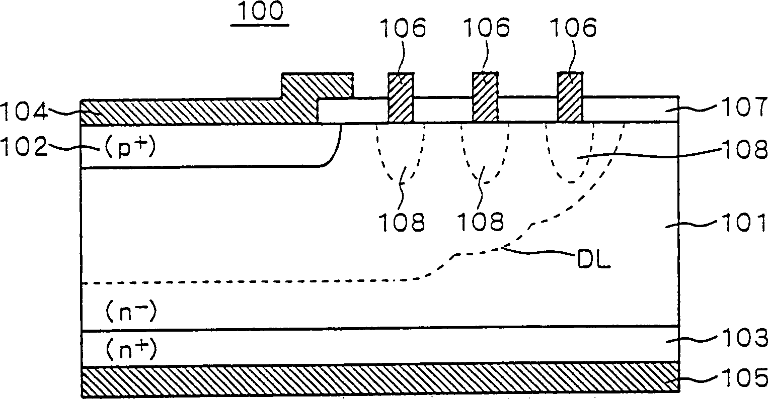
Wie
in
Ein
Siliziumoxidfilm
Weiterhin
ist eine n-dotierte Schicht
Bei
einer solchen Struktur tritt die Schottky-Metallschicht
Wenn
eine Rückwärtsvorspannung
an die Diode
B. HerstellungsverfahrenB. Manufacturing process
Ein
Verfahren zur Herstellung der Siliziumdiode
Zunächst wird
ein Siliziumsubstrat
Als
ein in
Nachdem
die Fotolackmaske RM11 entfernt wurde, wird eine n-Typ Dotierungs-Ionenart auf die andere
Hauptoberfläche
des Siliziumsubstrates
Als
ein in
Als
ein nächster
in
An
einem in
An
einem in
In
einem in
Wie
in
Jede
der ringförmigen
Schottky-Metallschichten
Zusätzlich dazu
sind die Anodenelektroden
Weiterhin
sind die Schottky-Metallschichten
Anstatt
den Siliziumoxidfilm
C Funktionsweise und EffektC operation and effect
Wie
oben beschrieben wurde, wird in dem erfindungsgemäßen Halbleiterelement
die Verarmungsregion
In Übereinstimmung damit ist es nicht notwendig, einen besonderen pn-Übergang in der Oberfläche des Halbleitersubstrates auszubilden, im Unterschied zu dem Fall, in welchem ein feldbegrenzender Ring als die Übergangsbeendigungsprozeßstruktur verwendet wird. Dadurch kann ein Herstellungsverfahren vereinfacht und die Herstellungskosten reduziert werden.In accordance so it is not necessary to make a special PN transition in the surface of the semiconductor substrate, unlike the case, in which a field-limiting ring as the transition completion process structure is used. This can simplify a manufacturing process and the manufacturing costs are reduced.
Im Unterschied zu dem Fall, in welchem ein SIPOS Film als die Übergangsbeendigungsprozeßstruktur verwendet wird, wird darüber hinaus eine Komponente, die eine große Temperaturabhängigkeit aufweist, nicht verwendet. Deswegen kann, selbst dann wenn eine Temperaturerhöhung erzeugt wird, ein Betrieb davor bewahrt werden, unkontrollierbar zu werden. Somit wird ein Halbleiterelement bereitgestellt, das eine hohe Verlässlichkeit aufweist.in the Difference to the case in which a SIPOS movie as the transition completion process structure is used is about it In addition, a component that has a large temperature dependence has not used. That's why, even if one temperature increase is generated, an operation to be prevented from being uncontrollable to become. Thus, a semiconductor element is provided which a high degree of reliability having.
D. VarianteD. variant
Während die
Siliziumdiode
Um ein Spannungssperrvermögen mit der Siliziumcarbiddiode zu erreichen, wird der feldbegrenzende Ring für die Übergangs- und Beendigungsprozessstruktur wie bereits beschrieben verwendet. Um den feldbegrenzenden Ring auf dem Siliziumcarbidsubstrat zu erzeugen, werden auch hier Ionen in das Siliziumcarbidsubstrat implantiert, das im Unterschied zum Siliziumsubstrat in einem hohen Temperaturzustand gehalten wird, und Aktivierung und thermische Diffusion werden bei Temperaturen von 1000 und mehreren 100 Grad ausgeführt. Wenn die erfin dungsgemäße Struktur aufgetragen wird, wird die Schottky Metallschicht wie ein Ring über die Hauptoberfläche des Siliziumcarbidsubstrates bereitgestellt. Damit kann die Herstellungsmethode vereinfacht werden, und eine Siliziumcarbiddiode, die ein Hochspannungssperrvermögen aufweist, wird in einer einfachen Weise zur Verfügung gestellt.In order to achieve voltage blocking capability with the silicon carbide diode, the field-limiting ring is used for the transition and termination process structure as previously described. Also, in order to produce the field-limiting ring on the silicon carbide substrate, ions are implanted in the silicon carbide substrate, which is kept in a high temperature state unlike the silicon substrate, and activation and thermal diffusion are carried out at temperatures of 1000 and several hundreds of degrees. When the structure of the present invention is applied, the Schottky metal layer is provided like a ring over the main surface of the silicon carbide substrate. Thus, the manufacturing method can unite become fuzzy, and a Siliziumcarbiddiode having a high voltage blocking capability is provided in a simple manner.
Während die Diode als ein Beispiel für ein Halbleiterelement in der oberen Beschreibung verwendet wurde, ist die hier dargestellte Erfindung nicht auf die Diode beschränkt, sondern kann für alle Halbleiterelemente, beispielsweise einen MOS-Transistor oder einen IGBT (insulated gate bipolar transistor) verwendet werden. Kurz gesagt, in dem Fall, in welchem eine Basisschicht eine Emitterschicht, eine Kollektorschicht und eine Quelle-Senke-Schicht oder derartiges in einer Hauptoberfläche einer zugrundeliegenden Halbleiterschicht ausgebildet wird, wird eine Verarmungsschicht, die von einem Hauptübergang gebildet wird, zur äußeren peripheren Seite ausgedehnt, ein maximales elektrisches Feld eines gekrümmten Teils des Hauptübergangs kann unterdrückt werden und eine Durchbruchsspannung kann gesteigert werden, wenn eine ringförmige Schottky-Metallschicht auf der Hauptoberfläche der zugrundeliegenden Halbleiterschicht um ein Gebiet herum angeordnet ist, in welchem die Schichten ausgebildet sind.While the Diode as an example of a semiconductor element was used in the above description, the invention presented here is not limited to the diode, but can for all semiconductor elements, such as a MOS transistor or an IGBT (insulated gate bipolar transistor) can be used. In short, in the case where a base layer has an emitter layer, a collector layer and a source-drain layer or the like in a main surface an underlying semiconductor layer is formed, is a Depletion layer formed by a main junction to the outer peripheral Extended side, a maximum electric field of a curved part the main transition can be suppressed and a breakdown voltage can be increased if an annular Schottky metal layer on the main surface the underlying semiconductor layer arranged around an area is, in which the layers are formed.
Obwohl die Erfindung in Einzelheiten dargestellt und beschrieben wurde, ist die hier dargestellte Beschreibung in allen Aspekten illustrativ und nicht beschränkend. Es ist verständlich, dass verschiedene Modifizierungen und Variationen ausgeführt werden können, ohne vom Blickwinkel der Erfindung hinwegzuführen.Even though the invention has been illustrated and described in detail, the description presented here is illustrative in all aspects and not restrictive. It is understandable, that various modifications and variations are made can, without departing from the scope of the invention.
Claims (6)
Applications Claiming Priority (2)
| Application Number | Priority Date | Filing Date | Title |
|---|---|---|---|
| JP2001251367A JP2003069045A (en) | 2001-08-22 | 2001-08-22 | Semiconductor device |
| JPP2001-251367 | 2001-08-22 |
Publications (2)
| Publication Number | Publication Date |
|---|---|
| DE10232425A1 DE10232425A1 (en) | 2003-03-13 |
| DE10232425B4 true DE10232425B4 (en) | 2007-03-29 |
Family
ID=19080024
Family Applications (1)
| Application Number | Title | Priority Date | Filing Date |
|---|---|---|---|
| DE10232425A Expired - Fee Related DE10232425B4 (en) | 2001-08-22 | 2002-07-17 | Semiconductor element |
Country Status (5)
| Country | Link |
|---|---|
| US (1) | US6670688B2 (en) |
| JP (1) | JP2003069045A (en) |
| KR (1) | KR100503936B1 (en) |
| CH (1) | CH696225A5 (en) |
| DE (1) | DE10232425B4 (en) |
Families Citing this family (13)
| Publication number | Priority date | Publication date | Assignee | Title |
|---|---|---|---|---|
| EP1619715A4 (en) * | 2003-04-25 | 2009-01-07 | Sumitomo Electric Industries | METHOD FOR PRODUCING SEMICONDUCTOR DEVICE |
| US7061021B2 (en) * | 2003-05-01 | 2006-06-13 | The University Of South Carolina | System and method for fabricating diodes |
| JP2006210667A (en) * | 2005-01-28 | 2006-08-10 | Mitsubishi Electric Corp | Semiconductor device |
| US7768092B2 (en) * | 2005-07-20 | 2010-08-03 | Cree Sweden Ab | Semiconductor device comprising a junction having a plurality of rings |
| JP4586775B2 (en) * | 2006-07-24 | 2010-11-24 | 日産自動車株式会社 | Silicon carbide semiconductor device |
| JP5090043B2 (en) * | 2007-03-30 | 2012-12-05 | オンセミコンダクター・トレーディング・リミテッド | diode |
| JP5195186B2 (en) * | 2008-09-05 | 2013-05-08 | 三菱電機株式会社 | Manufacturing method of semiconductor device |
| JP6026418B2 (en) * | 2010-09-27 | 2016-11-16 | アーベーベー・テヒノロギー・アーゲー | Bipolar non-punch-through power semiconductor device |
| US10283595B2 (en) * | 2015-04-10 | 2019-05-07 | Panasonic Corporation | Silicon carbide semiconductor substrate used to form semiconductor epitaxial layer thereon |
| JP6030806B1 (en) * | 2015-08-27 | 2016-11-24 | 新電元工業株式会社 | Wide gap type semiconductor device and method for manufacturing wide gap type semiconductor device |
| JP6519455B2 (en) * | 2015-11-26 | 2019-05-29 | 三菱電機株式会社 | Semiconductor device |
| JP2018018903A (en) * | 2016-07-26 | 2018-02-01 | トヨタ自動車株式会社 | Semiconductor device |
| EP3564995A1 (en) * | 2018-05-02 | 2019-11-06 | Université catholique de Louvain | Integrated circuit device and method of manufacturing thereof |
Citations (5)
| Publication number | Priority date | Publication date | Assignee | Title |
|---|---|---|---|---|
| US3760241A (en) * | 1969-06-21 | 1973-09-18 | Licentia Gmbh | Semiconductor device having a rectifying junction surrounded by a schottky contact |
| US4024564A (en) * | 1974-08-19 | 1977-05-17 | Sony Corporation | Semiconductor device having at least one PN junction and channel stopper surrounder by a protecture conducting layer |
| US4827324A (en) * | 1986-11-06 | 1989-05-02 | Siliconix Incorporated | Implantation of ions into an insulating layer to increase planar pn junction breakdown voltage |
| US4901120A (en) * | 1987-06-10 | 1990-02-13 | Unitrode Corporation | Structure for fast-recovery bipolar devices |
| DE19723176C1 (en) * | 1997-06-03 | 1998-08-27 | Daimler Benz Ag | Semiconductor device with alternate p-n and Schottky junctions |
Family Cites Families (10)
| Publication number | Priority date | Publication date | Assignee | Title |
|---|---|---|---|---|
| JPS556875A (en) | 1978-06-29 | 1980-01-18 | Nec Corp | Semiconductor device |
| JPS55120173A (en) * | 1979-03-12 | 1980-09-16 | Clarion Co Ltd | Schottky type variable capacitance diode with plural electrode structures |
| JPS5834944B2 (en) * | 1980-04-24 | 1983-07-29 | 日本電気株式会社 | semiconductor storage device |
| JPS6057945A (en) * | 1983-09-09 | 1985-04-03 | Fujitsu Ltd | Semiconductor device |
| JPS60241250A (en) * | 1984-05-15 | 1985-11-30 | Mitsubishi Electric Corp | Semiconductor device |
| JPH03185870A (en) * | 1989-12-15 | 1991-08-13 | Toshiba Corp | Semiconductor device |
| US5859465A (en) * | 1996-10-15 | 1999-01-12 | International Rectifier Corporation | High voltage power schottky with aluminum barrier metal spaced from first diffused ring |
| JPH11297994A (en) * | 1998-04-07 | 1999-10-29 | Hitachi Ltd | Semiconductor device |
| JP3185870B2 (en) | 1998-04-30 | 2001-07-11 | 日本電気株式会社 | High-speed, high-drive signal transmission circuit |
| JP3616258B2 (en) * | 1998-08-28 | 2005-02-02 | 株式会社ルネサステクノロジ | Schottky diode and power converter using the same |
-
2001
- 2001-08-22 JP JP2001251367A patent/JP2003069045A/en active Pending
-
2002
- 2002-06-07 US US10/163,996 patent/US6670688B2/en not_active Expired - Lifetime
- 2002-06-21 KR KR10-2002-0034867A patent/KR100503936B1/en not_active Expired - Fee Related
- 2002-07-15 CH CH01241/02A patent/CH696225A5/en not_active IP Right Cessation
- 2002-07-17 DE DE10232425A patent/DE10232425B4/en not_active Expired - Fee Related
Patent Citations (5)
| Publication number | Priority date | Publication date | Assignee | Title |
|---|---|---|---|---|
| US3760241A (en) * | 1969-06-21 | 1973-09-18 | Licentia Gmbh | Semiconductor device having a rectifying junction surrounded by a schottky contact |
| US4024564A (en) * | 1974-08-19 | 1977-05-17 | Sony Corporation | Semiconductor device having at least one PN junction and channel stopper surrounder by a protecture conducting layer |
| US4827324A (en) * | 1986-11-06 | 1989-05-02 | Siliconix Incorporated | Implantation of ions into an insulating layer to increase planar pn junction breakdown voltage |
| US4901120A (en) * | 1987-06-10 | 1990-02-13 | Unitrode Corporation | Structure for fast-recovery bipolar devices |
| DE19723176C1 (en) * | 1997-06-03 | 1998-08-27 | Daimler Benz Ag | Semiconductor device with alternate p-n and Schottky junctions |
Non-Patent Citations (1)
| Title |
|---|
| US 6501145 B1 (vorveröffentlicht als DE 197 23 176 C1) |
Also Published As
| Publication number | Publication date |
|---|---|
| KR20030017317A (en) | 2003-03-03 |
| DE10232425A1 (en) | 2003-03-13 |
| US20030038333A1 (en) | 2003-02-27 |
| US6670688B2 (en) | 2003-12-30 |
| CH696225A5 (en) | 2007-02-15 |
| JP2003069045A (en) | 2003-03-07 |
| KR100503936B1 (en) | 2005-07-27 |
Similar Documents
| Publication | Publication Date | Title |
|---|---|---|
| DE69602114T2 (en) | Trench field effect transistor with PN depletion layer barrier | |
| DE10214150B4 (en) | Silicon carbide semiconductor device and method of manufacturing the same | |
| EP1604404B1 (en) | Semiconductor structure comprising a highly doped conductive channel region and method for producing a semiconductor structure | |
| DE19701189B4 (en) | Semiconductor device | |
| DE19824514B4 (en) | diode | |
| DE10117350B4 (en) | Semiconductor arrangement and method for its production | |
| DE3878037T2 (en) | VERTICAL MOSFET WITH A VOLTAGE REGULATOR DIODE THAT IS NOT DEEP UNDER THE SURFACE. | |
| DE102018103973A1 (en) | SILICON CARBIDE SEMICONDUCTOR COMPONENT | |
| DE10203479A1 (en) | Semiconductor device | |
| DE102014101130B4 (en) | Reverse lock semiconductor device, semiconductor device with local emitter efficiency modification, and method of manufacturing a reverse lock semiconductor device | |
| DE19811297A1 (en) | Avalanche breakdown resistant MOS devices | |
| DE19900171B4 (en) | Silicon carbide semiconductor device and method for its production | |
| DE19913375A1 (en) | MOS transistor structure with a trench gate electrode and a reduced on-resistance and method for producing a MOS transistor structure | |
| DE2711562B2 (en) | Semiconductor component and method for its manufacture | |
| DE69629017T2 (en) | LATERAL THIN FILM SOI ARRANGEMENTS WITH A GRADED FIELD OXIDE AND LINEAR DOPING PROFILE | |
| DE102005018378B4 (en) | Semiconductor device of dielectric isolation type | |
| DE102014101859B4 (en) | Superjunction semiconductor device with overcompensation zones and method for their production | |
| EP0748520B1 (en) | Silicon carbide-based mis structure with high latch-up resistance | |
| DE19908477A1 (en) | Semiconductor component, e.g. free wheel diode (FWD), used as intelligent power module or component with doped substrate | |
| DE10232425A1 (en) | Semiconductor element | |
| DE69933645T2 (en) | LATERAL THIN-LAYER SOI ARRANGEMENT | |
| DE60028727T2 (en) | Manufacturing process for graded top oxide and drift area devices | |
| DE19818518C2 (en) | Semiconductor device and method for its production | |
| DE19641838A1 (en) | Termination structure for semiconductor components and method for producing such termination structures | |
| DE60030059T2 (en) | BREAKTHROUGH DIODE AND METHOD OF MANUFACTURE |
Legal Events
| Date | Code | Title | Description |
|---|---|---|---|
| OP8 | Request for examination as to paragraph 44 patent law | ||
| 8364 | No opposition during term of opposition | ||
| 8320 | Willingness to grant licences declared (paragraph 23) | ||
| R119 | Application deemed withdrawn, or ip right lapsed, due to non-payment of renewal fee |