EP0000070A1 - Druckkopf für Bildaufzeichnung - Google Patents
Druckkopf für Bildaufzeichnung Download PDFInfo
- Publication number
- EP0000070A1 EP0000070A1 EP78100129A EP78100129A EP0000070A1 EP 0000070 A1 EP0000070 A1 EP 0000070A1 EP 78100129 A EP78100129 A EP 78100129A EP 78100129 A EP78100129 A EP 78100129A EP 0000070 A1 EP0000070 A1 EP 0000070A1
- Authority
- EP
- European Patent Office
- Prior art keywords
- conductive
- network
- printing
- tapes
- ribbons
- Prior art date
- Legal status (The legal status is an assumption and is not a legal conclusion. Google has not performed a legal analysis and makes no representation as to the accuracy of the status listed.)
- Granted
Links
- 239000011159 matrix material Substances 0.000 claims description 20
- 239000000463 material Substances 0.000 claims description 17
- 239000004065 semiconductor Substances 0.000 claims description 17
- 239000004020 conductor Substances 0.000 claims description 6
- 229910052751 metal Inorganic materials 0.000 claims description 4
- 239000002184 metal Substances 0.000 claims description 4
- 230000003197 catalytic effect Effects 0.000 claims 2
- 230000005540 biological transmission Effects 0.000 abstract description 3
- 239000010410 layer Substances 0.000 description 9
- 235000012431 wafers Nutrition 0.000 description 8
- 241001422033 Thestylus Species 0.000 description 7
- 229910052709 silver Inorganic materials 0.000 description 6
- 239000004332 silver Substances 0.000 description 6
- 239000000853 adhesive Substances 0.000 description 4
- 230000001070 adhesive effect Effects 0.000 description 4
- 238000004040 coloring Methods 0.000 description 3
- 238000009434 installation Methods 0.000 description 3
- 239000008188 pellet Substances 0.000 description 3
- 238000004026 adhesive bonding Methods 0.000 description 2
- 238000010586 diagram Methods 0.000 description 2
- 238000009413 insulation Methods 0.000 description 2
- 238000000034 method Methods 0.000 description 2
- 230000004048 modification Effects 0.000 description 2
- 238000012986 modification Methods 0.000 description 2
- 230000003068 static effect Effects 0.000 description 2
- 229920002799 BoPET Polymers 0.000 description 1
- OKTJSMMVPCPJKN-UHFFFAOYSA-N Carbon Chemical compound [C] OKTJSMMVPCPJKN-UHFFFAOYSA-N 0.000 description 1
- RYGMFSIKBFXOCR-UHFFFAOYSA-N Copper Chemical compound [Cu] RYGMFSIKBFXOCR-UHFFFAOYSA-N 0.000 description 1
- 239000005041 Mylar™ Substances 0.000 description 1
- 230000009471 action Effects 0.000 description 1
- 230000001154 acute effect Effects 0.000 description 1
- 230000015572 biosynthetic process Effects 0.000 description 1
- 229910052799 carbon Inorganic materials 0.000 description 1
- 239000003054 catalyst Substances 0.000 description 1
- 238000006555 catalytic reaction Methods 0.000 description 1
- 230000008859 change Effects 0.000 description 1
- 238000006243 chemical reaction Methods 0.000 description 1
- 239000000470 constituent Substances 0.000 description 1
- 229910052802 copper Inorganic materials 0.000 description 1
- 239000010949 copper Substances 0.000 description 1
- 238000001514 detection method Methods 0.000 description 1
- 230000000694 effects Effects 0.000 description 1
- 238000005530 etching Methods 0.000 description 1
- 239000011521 glass Substances 0.000 description 1
- 239000011810 insulating material Substances 0.000 description 1
- 239000011229 interlayer Substances 0.000 description 1
- 238000012423 maintenance Methods 0.000 description 1
- 230000000873 masking effect Effects 0.000 description 1
- 238000001465 metallisation Methods 0.000 description 1
- 230000003287 optical effect Effects 0.000 description 1
- 230000008520 organization Effects 0.000 description 1
- 230000036961 partial effect Effects 0.000 description 1
- 235000010603 pastilles Nutrition 0.000 description 1
- 239000004033 plastic Substances 0.000 description 1
- 230000002829 reductive effect Effects 0.000 description 1
- 230000000717 retained effect Effects 0.000 description 1
- 230000035945 sensitivity Effects 0.000 description 1
- 238000010408 sweeping Methods 0.000 description 1
- 230000001360 synchronised effect Effects 0.000 description 1
- 239000002966 varnish Substances 0.000 description 1
- 238000003466 welding Methods 0.000 description 1
Images



Classifications
-
- H—ELECTRICITY
- H04—ELECTRIC COMMUNICATION TECHNIQUE
- H04N—PICTORIAL COMMUNICATION, e.g. TELEVISION
- H04N1/00—Scanning, transmission or reproduction of documents or the like, e.g. facsimile transmission; Details thereof
- H04N1/024—Details of scanning heads ; Means for illuminating the original
- H04N1/032—Details of scanning heads ; Means for illuminating the original for picture information reproduction
-
- B—PERFORMING OPERATIONS; TRANSPORTING
- B41—PRINTING; LINING MACHINES; TYPEWRITERS; STAMPS
- B41J—TYPEWRITERS; SELECTIVE PRINTING MECHANISMS, i.e. MECHANISMS PRINTING OTHERWISE THAN FROM A FORME; CORRECTION OF TYPOGRAPHICAL ERRORS
- B41J2/00—Typewriters or selective printing mechanisms characterised by the printing or marking process for which they are designed
- B41J2/385—Typewriters or selective printing mechanisms characterised by the printing or marking process for which they are designed characterised by selective supply of electric current or selective application of magnetism to a printing or impression-transfer material
- B41J2/425—Typewriters or selective printing mechanisms characterised by the printing or marking process for which they are designed characterised by selective supply of electric current or selective application of magnetism to a printing or impression-transfer material for removing surface layer selectively from electro-sensitive material, e.g. metal coated paper
-
- G—PHYSICS
- G01—MEASURING; TESTING
- G01D—MEASURING NOT SPECIALLY ADAPTED FOR A SPECIFIC VARIABLE; ARRANGEMENTS FOR MEASURING TWO OR MORE VARIABLES NOT COVERED IN A SINGLE OTHER SUBCLASS; TARIFF METERING APPARATUS; MEASURING OR TESTING NOT OTHERWISE PROVIDED FOR
- G01D15/00—Component parts of recorders for measuring arrangements not specially adapted for a specific variable
- G01D15/06—Electric recording elements, e.g. electrolytic
Definitions
- the present invention relates to a bar for printing an image on a sensitive paper.
- the printing bar is, in particular, used in a document reproduction station, belonging to a facsimile transmission installation.
- the reproduction of an analyzed document is ensured by a print head or bar, sweeping over sensitive paper chosen along successive lines.
- the head or strip is excited by the information signal received by the reproduction station and defining the content of the line scanned for printing the successive image points, along the scan line considered.
- the formation on the paper of image points, therefore of points of variable density, consists in triggering, by reaction, a localized modification of the paper used, so as to obtain a variation in its optical appearance, for example a coloring.
- the paper used at the receiving station can therefore be, for example, electro-sensitive, electro-catalytic or heat-sensitive.
- the paper used being, for example, electro-catalytic, the impression of a poirt of image is obtained by localized application on the paper of a stylus made of catalyst material chosen according to the paper and by passing a electric current between the stylus and the paper; this causes catalysis accompanied by a change in the coloring of the paper.
- the paper may consist of an outer layer of sensitive material, a conductive undercoat and a base paper supporting them.
- the stylus can for example be made of silver or covered with silver; it comes to bear on the outer layer.
- Printing of a full line of image can be accomplished by moving the single pen print head along the paper scan line.
- the printing of a complete scan line can also be obtained by a printing bar having as many printing pens as dots picture in line.
- the bar is static relative to the scan line considered, only a relative step-by-step movement of the paper and the bar will remain.
- Such a printing strip may comprise a first network of conductive ribbons insulated from each other and one end of each of which is linked to one of the styli and a second network of conductive ribbons, also isolated from each other. , connected to the first network to form several matrices.
- the object of the present invention is to constitute a multistylet printing bar equipped with matrices of elements allowing control of each of the styli and easy to carry out industrially.
- the addressing matrices of the styli are therefore integrated in the impression strip, at the level of the plates carrying or including the styli.
- the printing bar which will be described with reference to the appended drawing is intended for developing an image on sensitive paper, the printing of the image being obtained by scanning the paper along successive lines and printing successive image points along each line.
- the print bar fits into a facsimile reproduction unit, it is mechanically static, the paper sensitive on which is formed the image scrolling step by step, under the action of known drive means, facing the bar for printing successive scanning lines of the paper.
- the printing bar fits into a set of reproduction of documents belonging to a facsimile transmission installation. It allows an image definition of 1728 image points per scan line of 216 mm paper.
- the paper chosen is of the electro-catalytic type generally having a very high sensitivity, that is to say requiring only a low energy for its printing. This paper will, for example, have a clear initial appearance and the dark impression will be obtained by coloring.
- FIG. 1 an arrangement of the constituent elements of the printing bar has been illustrated.
- the bar is formed by a first network of conductive tapes 1, parallel and isolated from others.
- a first end 10 of each ribbon 1 is covered with a layer of material chosen according to the type of paper used, for example is covered with silver.
- This end 10 is the thermal part of the ribbon 1 or an intermediate part at the level of a folding of the ribbon'1.
- the end 10 forms a printing stylet designated below with the same reference 10.
- the conductive ribbons 1 will be 1728 in number; the 1,728 styli 10 extend regularly over 216 mm.
- the conductive tapes 1 are carried by a support 2, by means of an insulating plate 3.
- the support 2 is insulating and rigid; it will for example be made of glass or injected plastic.
- This support, at least 216 mm in length, is appropriately shaped: it has a section substantially in the shape of a rectangular trapezoid whose acute angle between the large base and the adjacent side has been rounded.
- the support 2 with a rounded tip is partly covered by the flexible and insulating plate 3.
- This plate 3 is secured to the support, for example by gluing. It extends over the length of the support, covering the large base of its section and projecting beyond the rounded tip.
- the support 2 has in section the shape of a rectangular trapezoid, with non-rounded point. It is, in part, covered by a rigid and insulating plate 4. This plate is secured to the support, for example by gluing. It extends over its entire length, on the edge forming the large base of its section, and projects beyond the tip of the support.
- FIGS. 1 and 2 and FIG. 3 the support and the plate which carry the conductive tapes (not illustrated in FIGS. 2 and 3) must make it possible, by their shape, to produce, between all of the styli (at the level of the rounded tip or at the free end of the rigid plate) and the surface of the paper, contacts located along a line.
- the first network of conductive ribbons 1 is produced on the wafer 3 (4) according to a technique close to that used for the constitution of printed circuits.
- this first network will be produced using masking and photoengraving techniques.
- the tapes 1 carried by the wafer are partly, at level of their end 10, covered with silver to constitute, after assembly of the wafer on the support, the respective styluses.
- the ribbons 1 may initially contain a percentage of silver to avoid this additional supply of silver at the ends forming the styli
- the print bar has a stylus addressing circuit. This addressing circuit is integrated in the bar.
- the bar includes a second support 5, made of material similar to that of the support 2.
- This second support 5 is of rectangular section. One of its large faces is covered with an insulating and flexible plate 6.
- This plate 6 is secured to the support 5, for example by bonding.
- This plate 6 carries a second network of conductive tapes 7 visible in the only FIG. 1.
- This second network of conductive tapes 7 is produced in a similar manner to the first network of conductive tapes 1.
- the conductive strips 7 of the second network are sixteen in number. They are parallel to each other and electrically isolated from each other. They extend over the length of the second support and its plate, that is to say at least 216 mm.
- the two networks of conductive strips 1 and 7 are orthogonal.
- the supports 2 and 5 being assembled to each other, the conductive tapes being interior, the conductors 1 and 7 constitute a matrix with lines formed by the ribbons 7 and columns formed by the ribbons 1.
- the lines designated by the same reference 7 and the columns designated by the same reference 1 are isolated from each other by a layer of insulating adhesive 8 deposited at least at each of the intersections between the rows and columns, except for certain intersections as will be seen below. This insulating adhesive 8 also ensures the assembly of the two supports 2 and 5 equipped.
- the preceding insulation at the intersections can, of course, be obtained by a layer of insulating varnish or an interlayer sheet of insulating material, for example of material known under the name Mylar, the sheet being suitably perforated to keep the intersections free of insulation. desired.
- the assembly of the fitted supports 2 and 5 can then be ensured by means of an insulating adhesive, for example inserted between the rows and / or the columns, or by a purely mechanical means.
- each conductive tape 1 carries a semiconductor part 11.
- These semiconductor parts 11 are stepped in height on the bar: sixteen semi parts successive conductors 11 are staged regularly substantially over the height of the bar and are arranged respectively opposite the sixteen conductive strips 7 with which they are in electrical contact. This same arrangement is retained for the following semiconductor parts taken in sets of sixteen; these semiconductor parts are carried respectively by the conductive tapes 1 divided into sets of sixteen. A diode D is thus formed between each strip 1 and a strip 7.
- Each conductive tape 1 is also in contact electric with a layer of resistive material 12, for example a carbon deposit.
- This resistive material 12 covers the second end of each ribbon 1 and extends over the wafer 3, extending the ribbon 1 considered.
- a resistor R is thus formed and connected in series on each ribbon 1.
- a conductive strip 13 covers the free ends of the resistive deposits 12 electrically connected to the ribbons 1 of the same assembly (sixteen ribbons 1). This conductive strip 13 will be connected to a first supply terminal (not illustrated in this FIG. 1) of the styli 10.
- the electrical circuit thus formed is shown in dashed lines: a ribbon 1, therefore the stylus 10, is supplied from the first supply terminal and from the strip 13, through the associated electrical resistance R.
- each set of 16 conductive tapes 1 has its own first supply terminal or its own hanger 13, and that, from a set of sixteen tapes 1 to another set, the first supply terminals, or the strips such as 13, are independent.
- the electrical circuit formed also includes the diode D connecting the conductive tape 1 considered to a conductive tape 7 whose free end is advantageously gilded and constitutes a second power supply terminal 14. This diode D allows or not to short-circuit the stylus 10 end of the ribbon 1 considered from the second supply terminal.
- a given ribbon 1 (column) is connected to a given ribbon 7 (line) through a diode, this ribbon 1 being isolated from the other ribbons 7 by the deposits 8.
- the conductive ribbons 1, 1728 in number will be produced in steps of 125 ⁇ .
- Each ribbon has a width of the order of 90 ⁇ ; note, however, that this dimension is not critical: it can be reduced to 30 ⁇ . approximately or increase it to 110 ⁇ .
- the conductive tapes 7, sixteen in number will for example have a pitch of 2 mm.
- the thickness of the layer of resistant material is hardly critical, its width will be close to that of the conductive tapes 1.
- the pieces of semiconductor material, in the form of a pellet have a diameter of a few tenths of a millimeter, for example of the order of 0.25 mm.
- FIG 4 there is illustrated, on a greatly enlarged scale, the mounting of the pieces of semiconductor material on the conductive tapes 1.
- the piece of semiconductor material 11 has the form of a pellet.
- the semiconductor patch is mounted on the ribbon 1 corresponding via a metal tip 15, ', for example copper.
- the strip 1 is widened as shown in 16 and if necessary has additional metallization for the proper fixing of the tip 15.
- the tip 15 is fixed at 16 to the tape 1 by welding, or by bonding using a conductive adhesive, and / or is held by pressure in the bar formed.
- the large diameter of the conductive patch relative to the small spacing between conductive tapes 1 requires, in fact, a transfer of the patch to the side of the conductive tapes 7 whose pitch is sufficient to avoid any contact between the semiconductor patch considered and the two strips 7 adjacent to the one which is electrically connected to it.
- the semiconductor pads 11 can be fixed to the tapes 7 at suitable locations, the electrical junction with the respective tapes 1 being provided by the metal pins 15 held by pressure or fixed on the tapes 1.
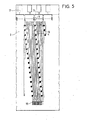
- the strips 1 a configuration such as that shown in FIG. 5.
- the locations of the diodes on the ribbons 1 are shown diagrammatically by small blackened circles designated by the aforementioned reference 16.
- the ribbons 1 carried by the plate 3 are compressed in gradation on either side of these locations 16.
- Each ribbon has a width of 50 to 80 ⁇ ; they are spaced from each other by 60 to 30 ⁇ .
- Sixteen successive ribbons 1 are thus formed. 2 mm wide, providing on each strip 1 the maximum dimension location 16 for a diode. This location can have 0.3 millimeter in diameter and can directly receive a semiconductor pellet. trice.
- FIG. 6 there is shown the electrical diagram of the printing bar including the stylus addressing circuit 10.
- the total bar is designated by 20.
- the addressing circuit which is integrated therein constitutes 108 diagonal dies 21, with diodes D each shown diagrammatically by a point on each of the sixteen junctions between sixteen columns and sixteen rows.
- the sixteen columns consist of the conductive tapes 1 of the same assembly and the sixteen rows by the sixteen conductive tapes 7.
- the sixteen columns, designated by the reference 1 are supplied respectively through the sixteen resistors R, from the supply terminal 17 connected to the resistors by the conductive strip 13.
- the supply terminals such as 17 are independent from one matrix to another.
- the sixteen lines are common to the 108 matrices 21. Each of the sixteen lines connects the diodes carried by the columns of the same rank belonging respectively to the 108 matrices. They are supplied from the supply terminals 14, these terminals 14 are independent of each other and each assigned to a line.
- the voltage applied to one of the terminals 17 will be 0 or 5 volts, that applied to one of the terminals 14 will be 0 or 5 volts;
- the first stylus of the first matrix 21 to be ordered for printing a black point we will put the terminal 17 of this first matrix under 5 volts, as well as the terminal 14 connected to the first line.
- the other terminals such as 17 supplying the columns of the other matrices, as well as the other terminals 14 connected to the other fifteen lines; will be set to 0 volts.
- the sixteen columns are under 5 volts by terminal 17.
- the diode D put under 5 volts will be blocked and will prevent the passage of current through the diode: the first stylus is therefore supplied and the current in this stylus causes a black dot to appear.
- the fifteen other diodes of this first matrix set to 0 volts are on: the residual current in these fifteen styli, due to the saturation voltage of the diodes, is very insufficient to cause an impression.
- all the diodes arranged on the first line considered are under 5 volts, this remains without effect since the columns of the other matrices are brought to 0 volt: the styli of the other matrices are not supplied.
- the diodes allow or not to short-circuit the styli of the same matrix, independently of each other. The diodes also make it possible to select a single matrix among the 108 existing matrices.
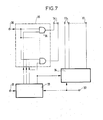
- This control circuit is shown having two control inputs.
- One of the inputs 30 receives the information signal for printing a line, composed of pulses of logic level 0 (0 volts) for printing a white point (stylus addressed but not controlled), or logic level 1 (5 volts) for printing a black dot (addressed and controlled stylus, that is to say crossed by a current).
- the input 31 receives clock pulses at the rate of printing of the dots along a scanning line of the paper.
- the information signal and the clock signal are synchronous.
- a third input of circuit 32 receives the synchronization signal at the start of the scanning line.
- the control circuit of the 108 matrices 21 includes a counter by 16, 33, connected to the input 31 receiving the clock signal.
- a counter by 108, 34 is connected to the row output 16 of the counter 33. It has 108 outputs connected respectively to the first 108 supply terminals 17 of the 108 matrices to allow their supply successively.
- the sixteen outputs of the counter 33 are connected to a combinational logic circuit 35 receiving the information signal from the input 30.
- This logic circuit 35 comprises sixteen AND gates such as 36, receiving on the one hand in parallel the information signal from the input 30 and connected on the other hand respectively to the sixteen outputs of the counter 33.
- the outputs of the sixteen AND gates 36 are respectively connected to the sixteen second supply terminals 14 of the 108 addressing matrices of the styluses.
- the line start synchronization signal ensures that the counter is forced by 108, 34, to state 1 for example on the detection of the end of this signal.
- the first matrix 21 has its sixteen columns placed under 5 volts. This same signal from terminal 32 ensures a forced reset of the counter by 16, 33.
- the clock pulses, which follow this line synchronization signal, advance the state of the counter by 16 for controlling the doors. AND 36 which are therefore successively passing for the information signal.
- state 1 of counter 33 the corresponding pulse of the information signal being at level 1 (black point), the first line of the 108 matrices will be put under 5 volts, the other lines being at 0 volt.
- the first stylus inscribes a black dot.
Landscapes
- Engineering & Computer Science (AREA)
- Multimedia (AREA)
- Signal Processing (AREA)
- Physics & Mathematics (AREA)
- General Physics & Mathematics (AREA)
- Dot-Matrix Printers And Others (AREA)
- Facsimile Heads (AREA)
- Electronic Switches (AREA)
- Printers Or Recording Devices Using Electromagnetic And Radiation Means (AREA)
- Electrophotography Using Other Than Carlson'S Method (AREA)
- Printing Plates And Materials Therefor (AREA)
Applications Claiming Priority (2)
| Application Number | Priority Date | Filing Date | Title |
|---|---|---|---|
| FR7718012A FR2394399A1 (fr) | 1977-06-13 | 1977-06-13 | Barrette d'impression d'une image |
| FR7718012 | 1977-06-13 |
Publications (2)
| Publication Number | Publication Date |
|---|---|
| EP0000070A1 true EP0000070A1 (de) | 1978-12-20 |
| EP0000070B1 EP0000070B1 (de) | 1981-02-18 |
Family
ID=9192020
Family Applications (1)
| Application Number | Title | Priority Date | Filing Date |
|---|---|---|---|
| EP78100129A Expired EP0000070B1 (de) | 1977-06-13 | 1978-06-08 | Druckkopf für Bildaufzeichnung |
Country Status (10)
| Country | Link |
|---|---|
| US (1) | US4180824A (de) |
| EP (1) | EP0000070B1 (de) |
| JP (1) | JPS5931938B2 (de) |
| BR (1) | BR7803769A (de) |
| CA (1) | CA1094145A (de) |
| DE (1) | DE2860532D1 (de) |
| DK (1) | DK145768C (de) |
| FR (1) | FR2394399A1 (de) |
| IE (1) | IE47086B1 (de) |
| IT (1) | IT1095162B (de) |
Cited By (2)
| Publication number | Priority date | Publication date | Assignee | Title |
|---|---|---|---|---|
| FR2501443A1 (fr) * | 1981-03-06 | 1982-09-10 | Cit Alcatel | Tete d'impression d'image |
| EP0124856A1 (de) * | 1983-05-09 | 1984-11-14 | Telic Alcatel | Elektrostatischer Druckkopf |
Families Citing this family (15)
| Publication number | Priority date | Publication date | Assignee | Title |
|---|---|---|---|---|
| JPS55109684A (en) * | 1979-02-16 | 1980-08-23 | Ricoh Co Ltd | Recorder |
| JPS5639675A (en) * | 1979-09-06 | 1981-04-15 | Ricoh Co Ltd | Facsimile equipment and its head |
| US4356501A (en) * | 1979-11-19 | 1982-10-26 | Xerox Corporation | Integrated silicon nib for an electrostatic printer |
| DE3143135C2 (de) * | 1981-10-28 | 1984-04-05 | Ingenieurbüro Dipl.-Ing. Hermann Künst, 1000 Berlin | Vielfachelektroden-Schreibkopf zum Aufzeichnen von Informationen auf einen Aufzeichnungsträger und Verfahren zur Herstellung eines Schreibkammes |
| FR2524389A1 (fr) * | 1982-04-02 | 1983-10-07 | Cit Alcatel | Tete d'impression electrostatique |
| JPS60155334U (ja) * | 1984-03-27 | 1985-10-16 | 有限会社 プラス歯材 | 歯間清掃具 |
| IL77906A (en) * | 1985-02-21 | 1989-09-28 | Butler John O Co | Interdental toothbrush |
| JPS61180014U (de) * | 1985-03-07 | 1986-11-10 | ||
| JPS61174427U (de) * | 1985-04-19 | 1986-10-30 | ||
| JPS6357944U (de) * | 1986-10-02 | 1988-04-18 | ||
| JPS6368822U (de) * | 1986-10-24 | 1988-05-09 | ||
| JPS6379731U (de) * | 1986-11-14 | 1988-05-26 | ||
| JPH01179526U (de) * | 1988-06-09 | 1989-12-22 | ||
| US5150134A (en) * | 1991-05-29 | 1992-09-22 | Xerox Corporation | Counter electrode for an electrostatic recorder |
| DE10040580A1 (de) | 2000-08-15 | 2002-02-28 | Heidelberger Druckmasch Ag | Vorrichtung zum Führen von Signaturen, insbesondere im Bereich eines Auslauf-Zwickels einer Schneidzylinderanordnung in einem Falzapparat einer Rotationsdruckmaschine |
Citations (5)
| Publication number | Priority date | Publication date | Assignee | Title |
|---|---|---|---|---|
| US2063992A (en) * | 1932-06-10 | 1936-12-15 | Westinghouse Electric & Mfg Co | Facsimile reception |
| FR1500533A (fr) * | 1965-10-24 | 1967-11-03 | Texas Instruments Inc | Dispositif d'affichage d'information |
| FR2110322A1 (de) * | 1970-10-09 | 1972-06-02 | Displaytek Corp | |
| US3903594A (en) * | 1974-05-28 | 1975-09-09 | Gould Inc | Method of making electrographic recording heads employing printed circuit techniques |
| GB1468258A (en) * | 1973-06-13 | 1977-03-23 | Tokyo Shibaura Electric Co | Electrostatic recorder |
Family Cites Families (8)
| Publication number | Priority date | Publication date | Assignee | Title |
|---|---|---|---|---|
| US2967083A (en) * | 1956-11-26 | 1961-01-03 | Radiation Inc | Fixed styli recording head |
| US3453647A (en) * | 1965-03-24 | 1969-07-01 | American Standard Inc | Thermographic recording apparatus |
| JPS5249310Y2 (de) * | 1972-01-19 | 1977-11-09 | ||
| US3827056A (en) * | 1972-10-04 | 1974-07-30 | Alden Res Found | Graphic electric recorder scanning device with printed recording strips |
| US4030107A (en) * | 1974-09-12 | 1977-06-14 | Sharp Kabushiki Kaisha | Electrographic recording devices employing electrostatic induction electrodes |
| US3984844A (en) * | 1974-11-20 | 1976-10-05 | Hitachi, Ltd. | Thermal recording apparatus |
| US4023184A (en) * | 1975-10-06 | 1977-05-10 | Mfe Corporation | Thermal matrix type printing head |
| DE2600340A1 (de) * | 1976-01-07 | 1977-08-25 | Sachs Elektronik Kg Hugo | Kammartige elektrodenanordnung |
-
1977
- 1977-06-13 FR FR7718012A patent/FR2394399A1/fr active Pending
-
1978
- 1978-06-08 DE DE7878100129T patent/DE2860532D1/de not_active Expired
- 1978-06-08 EP EP78100129A patent/EP0000070B1/de not_active Expired
- 1978-06-09 US US05/914,179 patent/US4180824A/en not_active Expired - Lifetime
- 1978-06-12 CA CA305,224A patent/CA1094145A/fr not_active Expired
- 1978-06-12 IT IT24456/78A patent/IT1095162B/it active
- 1978-06-12 IE IE1178/78A patent/IE47086B1/en unknown
- 1978-06-12 DK DK262378A patent/DK145768C/da not_active IP Right Cessation
- 1978-06-13 JP JP53070474A patent/JPS5931938B2/ja not_active Expired
- 1978-06-13 BR BR7803769A patent/BR7803769A/pt unknown
Patent Citations (5)
| Publication number | Priority date | Publication date | Assignee | Title |
|---|---|---|---|---|
| US2063992A (en) * | 1932-06-10 | 1936-12-15 | Westinghouse Electric & Mfg Co | Facsimile reception |
| FR1500533A (fr) * | 1965-10-24 | 1967-11-03 | Texas Instruments Inc | Dispositif d'affichage d'information |
| FR2110322A1 (de) * | 1970-10-09 | 1972-06-02 | Displaytek Corp | |
| GB1468258A (en) * | 1973-06-13 | 1977-03-23 | Tokyo Shibaura Electric Co | Electrostatic recorder |
| US3903594A (en) * | 1974-05-28 | 1975-09-09 | Gould Inc | Method of making electrographic recording heads employing printed circuit techniques |
Non-Patent Citations (1)
| Title |
|---|
| TECHNISCHE MITTEILLUNGEN AEG TELEFUNKEN, vol. 64, nr. 6, 1974, Berlin, SUESSENBACH "Grundlagen eines electrosensitiven Rasterdruckverfahrens", pages 193 à 197 * |
Cited By (5)
| Publication number | Priority date | Publication date | Assignee | Title |
|---|---|---|---|---|
| FR2501443A1 (fr) * | 1981-03-06 | 1982-09-10 | Cit Alcatel | Tete d'impression d'image |
| EP0059920A1 (de) * | 1981-03-06 | 1982-09-15 | COMPAGNIE INDUSTRIELLE DES TELECOMMUNICATIONS CIT-ALCATEL S.A. dite: | Bilddruckkopf |
| EP0124856A1 (de) * | 1983-05-09 | 1984-11-14 | Telic Alcatel | Elektrostatischer Druckkopf |
| FR2545759A1 (fr) * | 1983-05-09 | 1984-11-16 | Cit Alcatel | Tete d'impression electrostatique |
| US4636816A (en) * | 1983-05-09 | 1987-01-13 | Compagnie Industrielle Des Telecommunications Cit-Alcatel | Electrostatic print head |
Also Published As
| Publication number | Publication date |
|---|---|
| IE47086B1 (en) | 1983-12-14 |
| DK262378A (da) | 1978-12-14 |
| JPS546537A (en) | 1979-01-18 |
| FR2394399A1 (fr) | 1979-01-12 |
| JPS5931938B2 (ja) | 1984-08-06 |
| US4180824A (en) | 1979-12-25 |
| BR7803769A (pt) | 1979-01-09 |
| DK145768B (da) | 1983-02-21 |
| IE781178L (en) | 1978-12-13 |
| CA1094145A (fr) | 1981-01-20 |
| DE2860532D1 (en) | 1981-04-02 |
| DK145768C (da) | 1983-08-15 |
| IT7824456A0 (it) | 1978-06-12 |
| EP0000070B1 (de) | 1981-02-18 |
| IT1095162B (it) | 1985-08-10 |
Similar Documents
| Publication | Publication Date | Title |
|---|---|---|
| EP0000070B1 (de) | Druckkopf für Bildaufzeichnung | |
| EP0258130B1 (de) | Elektrolumineszierender flacher Bildschirm | |
| KR100954051B1 (ko) | 발광 소자 어레이 및 화상형성장치 | |
| EP0828452B1 (de) | Fingerabdrucksensor | |
| EP0362352B1 (de) | Belegleser | |
| EP0126110B1 (de) | Mit thermoelementen bestückter wärmeflussmesser | |
| FR2503432A1 (fr) | Dispositif d'affichage fluorescent | |
| EP0341121A1 (de) | Röntgenbilddetektor | |
| EP0000069B1 (de) | Druckkopf für Bildaufzeichnung | |
| FR2633420A1 (fr) | Support d'informations et systeme de gestion de tels supports | |
| EP0074869B1 (de) | Thermoelektrisches Anzeigegerät | |
| US4763136A (en) | Planar thermal head and display device incorporating the same | |
| JP2001260411A (ja) | 光プリンタヘッドおよびその点灯方法 | |
| FR2517864A1 (fr) | Dispositif d'enregistrement et de lecture d'images | |
| EP0124856B1 (de) | Elektrostatischer Druckkopf | |
| WO2003012869A2 (fr) | Panneau de visualisation d'images forme d'une matrice de cellules electroluminescentes a effet memoire | |
| EP3767261B1 (de) | Wärmemustersensor mit pixelmatrix mit heizschlangen | |
| EP0022704A1 (de) | Bildzeilendruckkopf, Verfahren zu seiner Herstellung und Bilddruckvorrrichtung | |
| EP0221453B1 (de) | Elektrostatischer Druckkopf | |
| JP2536477B2 (ja) | 印字記録装置 | |
| JPH07106536A (ja) | 受光素子アレイ及びその製造方法 | |
| FR2461415A1 (fr) | Barrette d'impression d'image et son procede de fabrication | |
| FR2531599A1 (fr) | Jonction multiple de fils tres etroitement espaces sur des substrats contigus | |
| EP4568103A1 (de) | Anschlussvorrichtung mit anpassbaren kontakten zur elektrischen prüfung einer solarzelle und prüfverfahren dafür | |
| WO2004011264A1 (fr) | Tete d'imprimante a haute densite |
Legal Events
| Date | Code | Title | Description |
|---|---|---|---|
| PUAI | Public reference made under article 153(3) epc to a published international application that has entered the european phase |
Free format text: ORIGINAL CODE: 0009012 |
|
| AK | Designated contracting states |
Kind code of ref document: A1 Designated state(s): BE DE FR GB LU NL SE |
|
| 17P | Request for examination filed | ||
| GRAA | (expected) grant |
Free format text: ORIGINAL CODE: 0009210 |
|
| AK | Designated contracting states |
Kind code of ref document: B1 Designated state(s): BE DE FR GB LU NL SE |
|
| REF | Corresponds to: |
Ref document number: 2860532 Country of ref document: DE Date of ref document: 19810402 |
|
| PG25 | Lapsed in a contracting state [announced via postgrant information from national office to epo] |
Ref country code: LU Free format text: LAPSE BECAUSE OF NON-PAYMENT OF DUE FEES Effective date: 19810630 |
|
| PGFP | Annual fee paid to national office [announced via postgrant information from national office to epo] |
Ref country code: LU Payment date: 19830518 Year of fee payment: 6 |
|
| PGFP | Annual fee paid to national office [announced via postgrant information from national office to epo] |
Ref country code: BE Payment date: 19840630 Year of fee payment: 7 Ref country code: SE Payment date: 19840630 Year of fee payment: 7 |
|
| PG25 | Lapsed in a contracting state [announced via postgrant information from national office to epo] |
Ref country code: SE Effective date: 19870609 |
|
| BERE | Be: lapsed |
Owner name: CIE INDUSTRIELLE DES TELECOMMUNICATIONS CIT-ALCA Effective date: 19870630 |
|
| PG25 | Lapsed in a contracting state [announced via postgrant information from national office to epo] |
Ref country code: BE Effective date: 19890630 |
|
| PGFP | Annual fee paid to national office [announced via postgrant information from national office to epo] |
Ref country code: GB Payment date: 19900418 Year of fee payment: 13 |
|
| PGFP | Annual fee paid to national office [announced via postgrant information from national office to epo] |
Ref country code: FR Payment date: 19900523 Year of fee payment: 13 |
|
| PGFP | Annual fee paid to national office [announced via postgrant information from national office to epo] |
Ref country code: DE Payment date: 19900626 Year of fee payment: 13 |
|
| PGFP | Annual fee paid to national office [announced via postgrant information from national office to epo] |
Ref country code: NL Payment date: 19900630 Year of fee payment: 13 |
|
| PG25 | Lapsed in a contracting state [announced via postgrant information from national office to epo] |
Ref country code: GB Effective date: 19910608 |
|
| PG25 | Lapsed in a contracting state [announced via postgrant information from national office to epo] |
Ref country code: NL Effective date: 19920101 |
|
| GBPC | Gb: european patent ceased through non-payment of renewal fee | ||
| NLV4 | Nl: lapsed or anulled due to non-payment of the annual fee | ||
| PG25 | Lapsed in a contracting state [announced via postgrant information from national office to epo] |
Ref country code: FR Effective date: 19920228 |
|
| PG25 | Lapsed in a contracting state [announced via postgrant information from national office to epo] |
Ref country code: DE Effective date: 19920401 |
|
| REG | Reference to a national code |
Ref country code: FR Ref legal event code: ST |
|
| EUG | Se: european patent has lapsed |
Ref document number: 78100129.2 Effective date: 19880711 |
|
| PLBE | No opposition filed within time limit |
Free format text: ORIGINAL CODE: 0009261 |
|
| STAA | Information on the status of an ep patent application or granted ep patent |
Free format text: STATUS: NO OPPOSITION FILED WITHIN TIME LIMIT |