EP0000647A1 - Commutateur optique pour deux guides d'ondes qui se croisent - Google Patents
Commutateur optique pour deux guides d'ondes qui se croisent Download PDFInfo
- Publication number
- EP0000647A1 EP0000647A1 EP78300172A EP78300172A EP0000647A1 EP 0000647 A1 EP0000647 A1 EP 0000647A1 EP 78300172 A EP78300172 A EP 78300172A EP 78300172 A EP78300172 A EP 78300172A EP 0000647 A1 EP0000647 A1 EP 0000647A1
- Authority
- EP
- European Patent Office
- Prior art keywords
- mode
- switch
- optical
- crosspoint
- wave energy
- Prior art date
- Legal status (The legal status is an assumption and is not a legal conclusion. Google has not performed a legal analysis and makes no representation as to the accuracy of the status listed.)
- Granted
Links
- 230000003287 optical effect Effects 0.000 title claims abstract description 42
- 238000011144 upstream manufacturing Methods 0.000 claims abstract 2
- 239000000758 substrate Substances 0.000 claims description 13
- 239000010409 thin film Substances 0.000 claims description 10
- 230000008878 coupling Effects 0.000 claims description 9
- 238000010168 coupling process Methods 0.000 claims description 9
- 238000005859 coupling reaction Methods 0.000 claims description 9
- 230000005415 magnetization Effects 0.000 claims description 4
- 238000006243 chemical reaction Methods 0.000 claims description 2
- 230000003319 supportive effect Effects 0.000 claims 2
- 239000000463 material Substances 0.000 claims 1
- 239000010408 film Substances 0.000 description 19
- 239000000835 fiber Substances 0.000 description 11
- 230000001902 propagating effect Effects 0.000 description 11
- 239000004020 conductor Substances 0.000 description 10
- 230000005284 excitation Effects 0.000 description 7
- 230000010287 polarization Effects 0.000 description 6
- 238000013461 design Methods 0.000 description 5
- 238000003780 insertion Methods 0.000 description 5
- 230000037431 insertion Effects 0.000 description 5
- 230000000694 effects Effects 0.000 description 4
- 238000000034 method Methods 0.000 description 4
- 239000002223 garnet Substances 0.000 description 3
- 230000003993 interaction Effects 0.000 description 3
- 239000011159 matrix material Substances 0.000 description 3
- WYTGDNHDOZPMIW-RCBQFDQVSA-N alstonine Natural products C1=CC2=C3C=CC=CC3=NC2=C2N1C[C@H]1[C@H](C)OC=C(C(=O)OC)[C@H]1C2 WYTGDNHDOZPMIW-RCBQFDQVSA-N 0.000 description 2
- 238000004519 manufacturing process Methods 0.000 description 2
- 239000013307 optical fiber Substances 0.000 description 2
- 229920002120 photoresistant polymer Polymers 0.000 description 2
- 238000012545 processing Methods 0.000 description 2
- VOXZDWNPVJITMN-ZBRFXRBCSA-N 17β-estradiol Chemical compound OC1=CC=C2[C@H]3CC[C@](C)([C@H](CC4)O)[C@@H]4[C@@H]3CCC2=C1 VOXZDWNPVJITMN-ZBRFXRBCSA-N 0.000 description 1
- 230000001154 acute effect Effects 0.000 description 1
- 230000005540 biological transmission Effects 0.000 description 1
- 239000000470 constituent Substances 0.000 description 1
- 239000013078 crystal Substances 0.000 description 1
- 230000001186 cumulative effect Effects 0.000 description 1
- 238000011161 development Methods 0.000 description 1
- 230000007717 exclusion Effects 0.000 description 1
- 230000006870 function Effects 0.000 description 1
- WABPQHHGFIMREM-VENIDDJXSA-N lead-201 Chemical compound [201Pb] WABPQHHGFIMREM-VENIDDJXSA-N 0.000 description 1
- WABPQHHGFIMREM-FTXFMUIASA-N lead-202 Chemical compound [202Pb] WABPQHHGFIMREM-FTXFMUIASA-N 0.000 description 1
- 239000012788 optical film Substances 0.000 description 1
- 230000000737 periodic effect Effects 0.000 description 1
- 238000000992 sputter etching Methods 0.000 description 1
Images


Classifications
-
- G—PHYSICS
- G02—OPTICS
- G02F—OPTICAL DEVICES OR ARRANGEMENTS FOR THE CONTROL OF LIGHT BY MODIFICATION OF THE OPTICAL PROPERTIES OF THE MEDIA OF THE ELEMENTS INVOLVED THEREIN; NON-LINEAR OPTICS; FREQUENCY-CHANGING OF LIGHT; OPTICAL LOGIC ELEMENTS; OPTICAL ANALOGUE/DIGITAL CONVERTERS
- G02F1/00—Devices or arrangements for the control of the intensity, colour, phase, polarisation or direction of light arriving from an independent light source, e.g. switching, gating or modulating; Non-linear optics
- G02F1/29—Devices or arrangements for the control of the intensity, colour, phase, polarisation or direction of light arriving from an independent light source, e.g. switching, gating or modulating; Non-linear optics for the control of the position or the direction of light beams, i.e. deflection
- G02F1/31—Digital deflection, i.e. optical switching
- G02F1/313—Digital deflection, i.e. optical switching in an optical waveguide structure
- G02F1/3137—Digital deflection, i.e. optical switching in an optical waveguide structure with intersecting or branching waveguides, e.g. X-switches and Y-junctions
-
- G—PHYSICS
- G02—OPTICS
- G02F—OPTICAL DEVICES OR ARRANGEMENTS FOR THE CONTROL OF LIGHT BY MODIFICATION OF THE OPTICAL PROPERTIES OF THE MEDIA OF THE ELEMENTS INVOLVED THEREIN; NON-LINEAR OPTICS; FREQUENCY-CHANGING OF LIGHT; OPTICAL LOGIC ELEMENTS; OPTICAL ANALOGUE/DIGITAL CONVERTERS
- G02F1/00—Devices or arrangements for the control of the intensity, colour, phase, polarisation or direction of light arriving from an independent light source, e.g. switching, gating or modulating; Non-linear optics
- G02F1/01—Devices or arrangements for the control of the intensity, colour, phase, polarisation or direction of light arriving from an independent light source, e.g. switching, gating or modulating; Non-linear optics for the control of the intensity, phase, polarisation or colour
- G02F1/09—Devices or arrangements for the control of the intensity, colour, phase, polarisation or direction of light arriving from an independent light source, e.g. switching, gating or modulating; Non-linear optics for the control of the intensity, phase, polarisation or colour based on magneto-optical elements, e.g. exhibiting Faraday effect
- G02F1/095—Devices or arrangements for the control of the intensity, colour, phase, polarisation or direction of light arriving from an independent light source, e.g. switching, gating or modulating; Non-linear optics for the control of the intensity, phase, polarisation or colour based on magneto-optical elements, e.g. exhibiting Faraday effect in an optical waveguide structure
-
- G—PHYSICS
- G02—OPTICS
- G02F—OPTICAL DEVICES OR ARRANGEMENTS FOR THE CONTROL OF LIGHT BY MODIFICATION OF THE OPTICAL PROPERTIES OF THE MEDIA OF THE ELEMENTS INVOLVED THEREIN; NON-LINEAR OPTICS; FREQUENCY-CHANGING OF LIGHT; OPTICAL LOGIC ELEMENTS; OPTICAL ANALOGUE/DIGITAL CONVERTERS
- G02F2201/00—Constructional arrangements not provided for in groups G02F1/00 - G02F7/00
- G02F2201/30—Constructional arrangements not provided for in groups G02F1/00 - G02F7/00 grating
- G02F2201/307—Reflective grating, i.e. Bragg grating
Definitions
- the invention relates to optical crosspoint switches for selectively redirecting optical wave energy from a first one to a second one of a pair of optical waveguiding channels.
- each of such proposed acoustic-optic arrangements has one or more disadvantages.
- separate piezoelectric transducers must be affixed to the lateral edges of the substrate at each of the crosspoints; this leads to a complicated and bulky assembly.
- the input and output channels are individually defined in parallel fashion on opposite surfaces of a common substrate.
- such design requires for its switching operation the physical movement of a pair of beam-guide couplers that are disposed at the opposite surfaces of the substrate.
- Optical crosspoint matrix designs using magneto-optic conversion have also been proposed. These designs have contemplated the use, at each crosspoint, of at least one directional coupler to extract only a portion of the incident energy for processing through the array.
- the Insertion loss exhibited by such scheme is relatively large and cumulative over the path of propagation of an optical beam through the device.
- a signal propagating in the second mode in the first channel and incident on the switch will, if the mode-switching means are inoperative, pass through the switch and continue propagating in the second mode in the first channel. If the mode-switching means are operative the signal will be converted to the first mode by the first mode-switching means, redirected to the second channel by the mode-sensitive means, and then be reconverted to the second mode by the second mode-switching means.
- the invention is particularly suited to fabrication by thin-film techniques and can be made inexpensively and with low insertion loss.
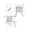
- FIG. 1 depicts generally an optical crosspoint switching array 11 including crosspoint switches in accordance with the invention.
- crosspoints designated 122-128 of the array 11 are illustrated for coupling one of a pair of input optical waveguides 132 and 134 to one of a pair of output optical waveguides 142 and 144.
- any desired number M x N of crosspoints may be provided in the array 11 for coupling one of M input waveguides to one of N output waveguides.
- the array 11 may illustratively form a part of an optical telephone communications system.
- the array 11 may be situated in a central office, while a unique input waveguide 132, 134 and a corresponding unique output waveguide 142, 144 may be assigned to one of the subscribers to such central office.
- a unique input waveguide 132, 134 and a corresponding unique output waveguide 142, 144 may be assigned to one of the subscribers to such central office.
- the operation of one of the crosspoints 12 within the matrix 11 e.g., by magneto-optic interaction in the manner to be described
- the waveguides 132, 142 may take the form of optical fibre transmission lines, and will be referred to as fibres in the following description.
- the crosspoints 122-124 are disposed at the intersections of discrete light paths through the array 11. In the particular arrangement of FIG. 1 and 2 such light paths are established as guided-mode channels through a thin planar optical film 21 disposed on a substrate 22.
- the film 21 is a magnetic single-crystal iron-garnet layer that is epitaxially grown on a chemically processed [1.1,1]Gd 3 Ga 5 O 12 substrate.
- a magnetic aniaotropy can be induced, with the easy axis thereof parallel to the plane of the film 21.
- the guided modes in the film may be restricted to the lowest-order TE and TM modes (designated TE a and TM o ). Such expedients are well known to those skilled in the art.
- Such arrangement of the film and substrate not only yields a large difference in refractive index therebetween relative to that which would normally be obtained if both the film and the substrate were isotropix, but also provides a large difference, within the film 21 itself., between the effective refractive indices respectively presented to the TE 0 and TM 0 modes.
- Optical energy from the output end of the fibre 132 is coupled, via a thin-film grating 32 fabricated on the surface of the film 21, onto a first guided-mode optical path 36.
- the optical wave energy from the fibre 132 impinges obliquely downwardly onto the grating 32, which converts a portion of the incident rays into the desired film-guided wave propagating along the path 36.
- a desired one of the TE and TM modes can be selected by the grating 32 as the polarization for the film-guided waves propagating along the light channel 36; and it will be assumedthat the polarization of the beam in the fiber 132 and the characteristics of the grating 32 are so chosen, in a conventional manner, that the TE a mode is selected for propagation along the path 36.
- the grating 32 may be constructed as described, e.g., in an article by M. L. Dackss et al, ''Grating Coupler for Efficient Excitation of Optical Guided Waves in Thin-Films", Applied Physics Letters, Vcl. 16, No. 12, pages 523-525 (June 15, 1970).
- the fabrication of the grating 32 may be accomplished by conventional holographic techniques, e.g., by exposing a photoresist layer on top of the film 21 to the interference of a collimated laser beam and a cylindrically focused beam.
- the photoresist grating which remains after development serves as a mask through which the grating may be replicated, by ion etching, onto the surface of the film.
- a thin-film grating 42 (FIG. 1) identical to the grating 32 may be defined on the film 21 for coupling light energy from the other illustrated input fiber 134 onto a second guided-mode light path 43 on the film 21.
- the polarization of the beam from the fiber 134, and the characteristics of the grating 42 are suitably chosen such that a TE a film-guided wave is launched in the light channel 43.
- a pair of output thin-film gratings 46, 47 are also fabricated in the film 21 for coupling light energy selectively routed through the array 11 to one of the output fibres 142 and 144 via light channels 51, 52.
- the grating 46 is effective to couple light energy, propagating in the TE 0 mode on the light channel 51, onto the output fibre 142
- the grating 47 is effective to couple light energy, propagating in the TE mode on the channel 52, onto the output fibre 144.
- the output light channel 51 intersects the input light channels 36, 43 at the crosspoints 122 and 126, respectively.
- the output light channel 52 intersects the input light channels 36, 43 at the crosspoints 124 and 128, respectively.
- the TE 0 mode launched onto the light path 36 from the input optical fibre 132 passes through a first magneto-optic selection switch 61 associated with the crosspoint 122.
- the switch 61 includes a photolithographically patterned, serpentine current conductor 62 (FIG. 3) which may be excited by current pulses as indicated below to produce a pulsed RF magnetic field that is directed along the path 36; such RF field is periodically reversed in direction as a result of the depicted geometry.
- Suitable DC biasing facilities may also be associated with the conductor 62 for establishing a steady magnetic field in the plane of the film 21 and directed at an acute angle (illustratively 45 degrees) to the axis of the light path 36. Because of the magnetic anisotropy caused, e.g., by the mismatch in lattice constant between the epitaxially grown iron-garnet film 21 and the underlying crystalline substrate 22, the total magnetization vector in the plane of the path 36 in the region encompassed by the conductor 62 may be rotated by the application of a relatively small magnetizing RF field in the conductor 62.
- such magnetization vector (which is normally oriented at 45 degrees to the path 36) can be periodically switched into a direction along the axis of the path 36. Also, with a suitable choice of the periodic constants of the conductor 62 and the strength of the total magnetization vector along the path 36 when the conductor 62 is pulsed, a significant portion of the T E0 mode energy normally propagating in the path 36 is converted into,the TM 0 mode.
- the current pulses for exciting the conductor 62 may illustratively be derived from a time-division switching pulse generator of the above-mentioned telephone communications systen. Such pulses are preferably selectively applied via parallel pulse inputs on an "X" lead 91 and a "Y" lead 92. Under non-coincident pulse conditions, the incoming TE 0 mode is not significantly affected, and proceeds unconverted through the switch 61 toward the intersection of the light paths 36 and 51.
- a second magneto-optic switch 101 identical to the switch 61, is associated with the crosspoint 122 and is positioned in the output light path 51 of the crosspoint.
- the switches 61 and 101 are arranged for joint excitation, and for this purpose the switch 101 is connected in series with the switch 61 by both the "X" lead 91 and the "Y" lead 92 as shown.
- a grating 121 is disposed at the intersection of the paths 36 and 51 in mode coupling relation to the associated magneto-optic switches 51 and 101.
- the grating 121 is preferably positioned at 45 degrees to the axes of each of the paths 36 and 51.
- the grating 121 may be fabricated holographically on the film 21 in a manner similar to that of the above-described input and output gratings 32, 42, 46 and 47 of the array 11.
- the attenuation constants presented thereby to incident TE O and TM 0 modes, respectively can be made to differ significantly; this effect is discussed, e.g., in Abstract F3 on page 21 of the Digest of Technical Papers for the 1972 International Quantum Electronics Conference.
- the grating 121 functions as an effective polarization mode filter, which presents a relatively low insertion loss to an incoming TE a wave while presenting a substantially totally reflecting interface to an incoming TM O wave. Since it is oriented at 45 degrees to the paths 36 and 57 as shown, the grating 121 will cause wave energy in the TM 0 mode to be directed from the incoming light path 36 into the intersecting light path 51.
- the transparency of such a 45 degree grating to the TE o mode is substantially independent of the direction of incidence of the wave energy; that is, the desired low insertion loss will be exhibitea whether the wave energy is propagating toward the crosspoint in one of the input waveguides 132, 134 or in one of the output waveguides 142, 144.
- the grating 121 will effect no significant interaction between optical beams simultaneously propagating toward the associated crosspoint in each of the constituent crossed optical paths.
- the crosspoint 122 in the operation of the crosspoint 122 as described above (e.g., consisting of a pair of magneto-optic switches 61 and 101 mode-coupled to the 45 degree grating 121 at the intersection of the paths 36 and 51), the functioning of such crosspoints in the absence of coincidence of current pulses on the leads 91 and 92 will first be described. Under such conditions, a guided TE 0 wave launched on the light path 36 from the fioer 132 will pass essentially unimpeded and unconverted through the magneto-optic switch 61 and will impinge on the grating 121 at the intersection.
- both of the serially-connected switches 61 and 101 at the crosspoint will be operated to convert optical wave energy incident thereon in one of the TE 0 and TM 0 modes into the other of such modes.
- wave energy in the TE 0 mode entering the crosspoint 122 on the path 36 will be initially converted, by the switch 61, into the TM 0 mode.
- the so-converted mode reaches the 45 degree grating 121 at the intersection of the paths 36 and 51, such mode will be reflected by the grating toward the other magneto-optic switch 101 in the path 51.
- Such switch reconverts the reflected TM O mode to the TE 0 mode, which in turn will pass freely through the remaining unaperated crosspoints (e.g., the crosspoint 126) disposed in the path 51 to be coupled onto the output fibre 142.
- an additional "X" lead 201 extends through all of the crosspoints in the light path 43, while an auxiliary “Y” lead 202 extends through all of the crosspoints in the light path 52. It will be understood that the coincident excitation of a desired pair of tne illustrated leads "X", "Y" will operate only the associated crosspoint.
- a speech path may be maintained through such crosspoint from an input subscribers fiber 132,134 to an output subscribers fiber 142,144 until the state of the associated magneto-optic switches is changed.
- Such change may be accomplished, e.g., by suitably pulsing the associated X-Y leads with the opposite polarity.
Landscapes
- Physics & Mathematics (AREA)
- Nonlinear Science (AREA)
- General Physics & Mathematics (AREA)
- Optics & Photonics (AREA)
- Engineering & Computer Science (AREA)
- Power Engineering (AREA)
- Optical Integrated Circuits (AREA)
Applications Claiming Priority (2)
| Application Number | Priority Date | Filing Date | Title |
|---|---|---|---|
| US05/818,670 US4153329A (en) | 1977-07-25 | 1977-07-25 | Optical crosspoint switch having mode-conversion facilities |
| US818670 | 1977-07-25 |
Publications (2)
| Publication Number | Publication Date |
|---|---|
| EP0000647A1 true EP0000647A1 (fr) | 1979-02-07 |
| EP0000647B1 EP0000647B1 (fr) | 1981-04-29 |
Family
ID=25226115
Family Applications (1)
| Application Number | Title | Priority Date | Filing Date |
|---|---|---|---|
| EP78300172A Expired EP0000647B1 (fr) | 1977-07-25 | 1978-07-20 | Commutateur optique pour deux guides d'ondes qui se croisent |
Country Status (5)
| Country | Link |
|---|---|
| US (1) | US4153329A (fr) |
| EP (1) | EP0000647B1 (fr) |
| JP (2) | JPS5424048A (fr) |
| CA (1) | CA1105602A (fr) |
| DE (1) | DE2860646D1 (fr) |
Cited By (4)
| Publication number | Priority date | Publication date | Assignee | Title |
|---|---|---|---|---|
| US4223977A (en) * | 1978-04-25 | 1980-09-23 | Thomson-Csf | Integrated optical demultiplexing circuit |
| EP0037793A3 (en) * | 1980-03-31 | 1982-03-24 | Polaroid Corporation | Communications tuning construction |
| CN102566040A (zh) * | 2010-12-27 | 2012-07-11 | 上海丽恒光微电子科技有限公司 | Mems显示器 |
| US20190072035A1 (en) * | 2017-09-06 | 2019-03-07 | Rolls-Royce Plc | Heat exchange systems for turbomachines |
Families Citing this family (24)
| Publication number | Priority date | Publication date | Assignee | Title |
|---|---|---|---|---|
| FR2403567A1 (fr) * | 1977-09-16 | 1979-04-13 | Thomson Csf | Dispositif de transmission de rayonnements optiques et son application au multiplexage-demultiplexage d'ondes porteuses optiques |
| FR2411426A1 (fr) * | 1977-12-09 | 1979-07-06 | Thomson Csf | Bifurcation optique a commande electrique et son application aux dispositifs de transmission par fibres optiques |
| US4384760A (en) * | 1980-12-15 | 1983-05-24 | Bell Telephone Laboratories, Incorporated | Polarization transformer |
| US4444460A (en) * | 1981-05-26 | 1984-04-24 | Gould Inc. | Optical fiber apparatus including subtstrate ruggedized optical fibers |
| US4545078A (en) * | 1981-11-27 | 1985-10-01 | Siemens Aktiengesellschaft | Method and arrangement for controlling a light switch for optical signals |
| FR2538127B1 (fr) * | 1982-12-21 | 1986-01-24 | Socapex | Quadripole optique et multipole comportant de tels quadripoles |
| FR2546309B1 (fr) * | 1983-05-19 | 1986-07-04 | Yi Yan Alfredo | Structure de guidage optique utilisant un reseau de diffraction |
| NL8303446A (nl) * | 1983-10-07 | 1985-05-01 | Philips Nv | Component voor een geintegreerd optisch systeem. |
| US4580873A (en) * | 1983-12-30 | 1986-04-08 | At&T Bell Laboratories | Optical matrix switch |
| DE3587515T2 (de) * | 1984-05-17 | 1994-03-17 | Nippon Electric Co | Optische Schalteinrichtung. |
| GB8516108D0 (en) * | 1985-06-26 | 1985-07-31 | Gen Electric Co Plc | Optical switch |
| US4761832A (en) * | 1985-06-28 | 1988-08-02 | Amp Incorporated | Fiber optic switching network |
| US4717230A (en) * | 1985-06-28 | 1988-01-05 | Amp Incorporated | Optical eraser and node switch for an optical network |
| US4681397A (en) * | 1985-06-28 | 1987-07-21 | Amp Incorporated | Optical switching arrangement |
| FR2584825B1 (fr) * | 1985-07-11 | 1987-10-09 | Labo Electronique Physique | Structure separatrice, element de commutation optique incluant de telles structures et matrice de commutation optique formee de ces elements de commutation |
| JPH0776811B2 (ja) * | 1986-05-06 | 1995-08-16 | 三菱電機株式会社 | 磁気光学装置 |
| GB2196503A (en) * | 1986-10-15 | 1988-04-27 | Plessey Co Plc | An arrangement for linking multistage switching matrices |
| FR2621401B1 (fr) * | 1987-10-02 | 1989-12-29 | Labo Electronique Physique | Element de commutation optique incluant deux guides de lumiere paralleles et matrice de commutation constituee de tels elements |
| US4931635A (en) * | 1987-12-01 | 1990-06-05 | Teijin Seiki Company Limited | Optical position sensor using Faraday effect element and magnetic scale |
| US5544268A (en) * | 1994-09-09 | 1996-08-06 | Deacon Research | Display panel with electrically-controlled waveguide-routing |
| US6118911A (en) * | 1998-09-25 | 2000-09-12 | Hughes Electronics Corporation | Waveguide switch matrix using junctions matched in only one state |
| US7183633B2 (en) * | 2001-03-01 | 2007-02-27 | Analog Devices Inc. | Optical cross-connect system |
| US6873756B2 (en) | 2001-09-07 | 2005-03-29 | Analog Devices, Inc. | Tiling of optical MEMS devices |
| US6842553B2 (en) | 2001-04-17 | 2005-01-11 | Creo Srl | Method for cross-connecting optical signals at high speed |
Citations (3)
| Publication number | Priority date | Publication date | Assignee | Title |
|---|---|---|---|---|
| US3764195A (en) * | 1972-02-02 | 1973-10-09 | Bell Telephone Labor Inc | Optical waveguide devices using single-crystal garnet films |
| US3990776A (en) * | 1975-06-17 | 1976-11-09 | International Business Machines Corporation | Magneto-optical digital light deflector |
| US4011543A (en) * | 1976-02-20 | 1977-03-08 | Sperry Rand Corporation | Low crosstalk optical switch |
Family Cites Families (3)
| Publication number | Priority date | Publication date | Assignee | Title |
|---|---|---|---|---|
| US3870397A (en) * | 1973-11-13 | 1975-03-11 | Bell Telephone Labor Inc | Thin film magneto-optic switch |
| US4032216A (en) * | 1976-03-15 | 1977-06-28 | Rockwell International Corporation | Thin film magneto-optic mode converters |
| JPS53148A (en) * | 1976-06-24 | 1978-01-05 | Mitsubishi Electric Corp | Optical switch matrix |
-
1977
- 1977-07-25 US US05/818,670 patent/US4153329A/en not_active Expired - Lifetime
-
1978
- 1978-07-13 CA CA307,328A patent/CA1105602A/fr not_active Expired
- 1978-07-20 DE DE7878300172T patent/DE2860646D1/de not_active Expired
- 1978-07-20 EP EP78300172A patent/EP0000647B1/fr not_active Expired
- 1978-07-25 JP JP9007078A patent/JPS5424048A/ja active Pending
-
1985
- 1985-04-22 JP JP1985058966U patent/JPS60184022U/ja active Pending
Patent Citations (3)
| Publication number | Priority date | Publication date | Assignee | Title |
|---|---|---|---|---|
| US3764195A (en) * | 1972-02-02 | 1973-10-09 | Bell Telephone Labor Inc | Optical waveguide devices using single-crystal garnet films |
| US3990776A (en) * | 1975-06-17 | 1976-11-09 | International Business Machines Corporation | Magneto-optical digital light deflector |
| US4011543A (en) * | 1976-02-20 | 1977-03-08 | Sperry Rand Corporation | Low crosstalk optical switch |
Non-Patent Citations (1)
| Title |
|---|
| JOURNAL OF APPLIED PHYSICS, vol. 45, no. 2, February 1974, New York, (US) S. YAMAMOTO et al.: "Circuit theory for a class of antisotropic and gyrotropic thin-film optical waveguides and design of nonreciprocal devices for integrated optics", pages 882-888 * |
Cited By (5)
| Publication number | Priority date | Publication date | Assignee | Title |
|---|---|---|---|---|
| US4223977A (en) * | 1978-04-25 | 1980-09-23 | Thomson-Csf | Integrated optical demultiplexing circuit |
| EP0037793A3 (en) * | 1980-03-31 | 1982-03-24 | Polaroid Corporation | Communications tuning construction |
| CN102566040A (zh) * | 2010-12-27 | 2012-07-11 | 上海丽恒光微电子科技有限公司 | Mems显示器 |
| CN102566040B (zh) * | 2010-12-27 | 2014-01-08 | 上海丽恒光微电子科技有限公司 | Mems显示器 |
| US20190072035A1 (en) * | 2017-09-06 | 2019-03-07 | Rolls-Royce Plc | Heat exchange systems for turbomachines |
Also Published As
| Publication number | Publication date |
|---|---|
| CA1105602A (fr) | 1981-07-21 |
| EP0000647B1 (fr) | 1981-04-29 |
| US4153329A (en) | 1979-05-08 |
| JPS60184022U (ja) | 1985-12-06 |
| JPS5424048A (en) | 1979-02-23 |
| DE2860646D1 (en) | 1981-08-06 |
Similar Documents
| Publication | Publication Date | Title |
|---|---|---|
| EP0000647B1 (fr) | Commutateur optique pour deux guides d'ondes qui se croisent | |
| US4355864A (en) | Magnetooptic switching devices | |
| US5165104A (en) | Optical interconnecting device and method | |
| US4828362A (en) | Optical switch | |
| US3920314A (en) | Mode conversion and mode separation branched dielectric waveguide element for light | |
| US4130342A (en) | Passive optical channel crossover, switch and bend structure | |
| US4143941A (en) | Low loss optical data terminal device for multimode fiber guide optical communication systems | |
| US3909108A (en) | Optical switch and modulator | |
| EP0677174A1 (fr) | Procede de modification des rapports d'intensite et de phase dans des coupleurs multimodes a interferences | |
| EP0936489B1 (fr) | Circulateur optique | |
| GB1576595A (en) | Optical waveguide system for electrically controlling the transmission of optical radiation | |
| EP0335672A2 (fr) | Commutateur à guide d'onde optique indépendant de la polarisation | |
| JPS63197923A (ja) | マトリツクス光スイツチ | |
| DE69800016T2 (de) | Akustooptischer Schalter für optische Wellenleiterstruktur aus Siliziumdioxid | |
| US6112000A (en) | Reflective array multiplexer with polarization compensation | |
| Ramer et al. | Experimental integrated optic circuit losses and fiber pigtailing of chips | |
| US4995693A (en) | Multi-position opto-electronic switch | |
| EP0821263B1 (fr) | Elément de branchement optique non-linéaire | |
| US6360034B1 (en) | Reflection based nonmoving part optical switch | |
| US6510259B1 (en) | Optical switch using an integrated Mach-Zehnder interferometer having a movable phase shifter and asymmetric arms | |
| US6842573B2 (en) | Directional optical coupler | |
| Shirasaki et al. | Magnetooptical 2× 2 switch for single-mode fibers | |
| Tietgen et al. | 180°-turns in integrated optics | |
| JPH01225905A (ja) | 光導波路 | |
| JP3379658B2 (ja) | 光スイッチ |
Legal Events
| Date | Code | Title | Description |
|---|---|---|---|
| PUAI | Public reference made under article 153(3) epc to a published international application that has entered the european phase |
Free format text: ORIGINAL CODE: 0009012 |
|
| AK | Designated contracting states |
Designated state(s): BE DE FR GB NL SE |
|
| 17P | Request for examination filed | ||
| GRAA | (expected) grant |
Free format text: ORIGINAL CODE: 0009210 |
|
| AK | Designated contracting states |
Designated state(s): BE DE FR GB NL SE |
|
| REF | Corresponds to: |
Ref document number: 2860646 Country of ref document: DE Date of ref document: 19810806 |
|
| PGFP | Annual fee paid to national office [announced via postgrant information from national office to epo] |
Ref country code: DE Payment date: 19840625 Year of fee payment: 7 |
|
| PGFP | Annual fee paid to national office [announced via postgrant information from national office to epo] |
Ref country code: SE Payment date: 19840630 Year of fee payment: 7 Ref country code: BE Payment date: 19840630 Year of fee payment: 7 |
|
| PGFP | Annual fee paid to national office [announced via postgrant information from national office to epo] |
Ref country code: FR Payment date: 19840703 Year of fee payment: 7 |
|
| PGFP | Annual fee paid to national office [announced via postgrant information from national office to epo] |
Ref country code: NL Payment date: 19860731 Year of fee payment: 9 |
|
| PG25 | Lapsed in a contracting state [announced via postgrant information from national office to epo] |
Ref country code: SE Effective date: 19870721 |
|
| BERE | Be: lapsed |
Owner name: WESTERN ELECTRIC CY INC. Effective date: 19870731 |
|
| PG25 | Lapsed in a contracting state [announced via postgrant information from national office to epo] |
Ref country code: NL Effective date: 19880201 |
|
| NLV4 | Nl: lapsed or anulled due to non-payment of the annual fee | ||
| PG25 | Lapsed in a contracting state [announced via postgrant information from national office to epo] |
Ref country code: FR Free format text: LAPSE BECAUSE OF NON-PAYMENT OF DUE FEES Effective date: 19880331 |
|
| PG25 | Lapsed in a contracting state [announced via postgrant information from national office to epo] |
Ref country code: DE Effective date: 19880401 |
|
| GBPC | Gb: european patent ceased through non-payment of renewal fee | ||
| REG | Reference to a national code |
Ref country code: FR Ref legal event code: ST |
|
| PG25 | Lapsed in a contracting state [announced via postgrant information from national office to epo] |
Ref country code: GB Free format text: LAPSE BECAUSE OF NON-PAYMENT OF DUE FEES Effective date: 19881117 |
|
| PG25 | Lapsed in a contracting state [announced via postgrant information from national office to epo] |
Ref country code: BE Effective date: 19890731 |
|
| EUG | Se: european patent has lapsed |
Ref document number: 78300172.0 Effective date: 19880713 |
|
| PLBE | No opposition filed within time limit |
Free format text: ORIGINAL CODE: 0009261 |
|
| STAA | Information on the status of an ep patent application or granted ep patent |
Free format text: STATUS: NO OPPOSITION FILED WITHIN TIME LIMIT |