EP0004824A2 - Messerkontakt und Verfahren zum Aufbringen einer Nickelschicht auf ein Aluminiumstück - Google Patents
Messerkontakt und Verfahren zum Aufbringen einer Nickelschicht auf ein Aluminiumstück Download PDFInfo
- Publication number
- EP0004824A2 EP0004824A2 EP79420015A EP79420015A EP0004824A2 EP 0004824 A2 EP0004824 A2 EP 0004824A2 EP 79420015 A EP79420015 A EP 79420015A EP 79420015 A EP79420015 A EP 79420015A EP 0004824 A2 EP0004824 A2 EP 0004824A2
- Authority
- EP
- European Patent Office
- Prior art keywords
- nickel
- contact
- aluminum
- layer
- coated
- Prior art date
- Legal status (The legal status is an assumption and is not a legal conclusion. Google has not performed a legal analysis and makes no representation as to the accuracy of the status listed.)
- Granted
Links
- PXHVJJICTQNCMI-UHFFFAOYSA-N Nickel Chemical compound [Ni] PXHVJJICTQNCMI-UHFFFAOYSA-N 0.000 title claims abstract description 128
- 229910052759 nickel Inorganic materials 0.000 title claims abstract description 64
- 229910052782 aluminium Inorganic materials 0.000 title claims abstract description 38
- XAGFODPZIPBFFR-UHFFFAOYSA-N aluminium Chemical compound [Al] XAGFODPZIPBFFR-UHFFFAOYSA-N 0.000 title claims abstract description 38
- 238000000034 method Methods 0.000 title claims abstract description 26
- 238000000576 coating method Methods 0.000 title claims description 15
- 239000011248 coating agent Substances 0.000 title claims description 11
- 239000004020 conductor Substances 0.000 title claims description 10
- 239000004411 aluminium Substances 0.000 title description 2
- 229910052709 silver Inorganic materials 0.000 claims abstract description 27
- 239000004332 silver Substances 0.000 claims abstract description 26
- AZDRQVAHHNSJOQ-UHFFFAOYSA-N alumane Chemical group [AlH3] AZDRQVAHHNSJOQ-UHFFFAOYSA-N 0.000 claims abstract description 10
- 239000000758 substrate Substances 0.000 claims abstract description 10
- 230000008646 thermal stress Effects 0.000 claims abstract description 5
- 239000010410 layer Substances 0.000 claims description 32
- 230000008021 deposition Effects 0.000 claims description 17
- 238000004519 manufacturing process Methods 0.000 claims description 11
- 230000008569 process Effects 0.000 claims description 6
- 239000011247 coating layer Substances 0.000 claims description 3
- 238000005554 pickling Methods 0.000 claims description 3
- 230000003068 static effect Effects 0.000 claims description 2
- 229910021586 Nickel(II) chloride Inorganic materials 0.000 claims 1
- KGBXLFKZBHKPEV-UHFFFAOYSA-N boric acid Chemical compound OB(O)O KGBXLFKZBHKPEV-UHFFFAOYSA-N 0.000 claims 1
- 239000004327 boric acid Substances 0.000 claims 1
- XIKYYQJBTPYKSG-UHFFFAOYSA-N nickel Chemical compound [Ni].[Ni] XIKYYQJBTPYKSG-UHFFFAOYSA-N 0.000 claims 1
- QMMRZOWCJAIUJA-UHFFFAOYSA-L nickel dichloride Chemical compound Cl[Ni]Cl QMMRZOWCJAIUJA-UHFFFAOYSA-L 0.000 claims 1
- KERTUBUCQCSNJU-UHFFFAOYSA-L nickel(2+);disulfamate Chemical compound [Ni+2].NS([O-])(=O)=O.NS([O-])(=O)=O KERTUBUCQCSNJU-UHFFFAOYSA-L 0.000 claims 1
- 239000011241 protective layer Substances 0.000 claims 1
- BQCADISMDOOEFD-UHFFFAOYSA-N Silver Chemical compound [Ag] BQCADISMDOOEFD-UHFFFAOYSA-N 0.000 abstract description 24
- 238000000151 deposition Methods 0.000 abstract description 14
- 235000010210 aluminium Nutrition 0.000 description 30
- RYGMFSIKBFXOCR-UHFFFAOYSA-N Copper Chemical compound [Cu] RYGMFSIKBFXOCR-UHFFFAOYSA-N 0.000 description 21
- 239000010949 copper Substances 0.000 description 21
- 229910052802 copper Inorganic materials 0.000 description 20
- ATJFFYVFTNAWJD-UHFFFAOYSA-N Tin Chemical compound [Sn] ATJFFYVFTNAWJD-UHFFFAOYSA-N 0.000 description 16
- 238000012360 testing method Methods 0.000 description 16
- 239000011135 tin Substances 0.000 description 16
- 229910052718 tin Inorganic materials 0.000 description 16
- 229910045601 alloy Inorganic materials 0.000 description 10
- 239000000956 alloy Substances 0.000 description 10
- 229910052751 metal Inorganic materials 0.000 description 8
- 239000002184 metal Substances 0.000 description 8
- 239000000243 solution Substances 0.000 description 6
- 239000007864 aqueous solution Substances 0.000 description 5
- 150000002739 metals Chemical class 0.000 description 5
- 239000008188 pellet Substances 0.000 description 5
- 238000011282 treatment Methods 0.000 description 5
- HCHKCACWOHOZIP-UHFFFAOYSA-N Zinc Chemical compound [Zn] HCHKCACWOHOZIP-UHFFFAOYSA-N 0.000 description 4
- 230000008901 benefit Effects 0.000 description 4
- 230000015556 catabolic process Effects 0.000 description 4
- 230000003647 oxidation Effects 0.000 description 4
- 238000007254 oxidation reaction Methods 0.000 description 4
- 229910052725 zinc Inorganic materials 0.000 description 4
- 239000011701 zinc Substances 0.000 description 4
- 229910000906 Bronze Inorganic materials 0.000 description 3
- 238000005299 abrasion Methods 0.000 description 3
- 230000032683 aging Effects 0.000 description 3
- 238000005219 brazing Methods 0.000 description 3
- 239000010974 bronze Substances 0.000 description 3
- 230000006835 compression Effects 0.000 description 3
- 238000007906 compression Methods 0.000 description 3
- KUNSUQLRTQLHQQ-UHFFFAOYSA-N copper tin Chemical compound [Cu].[Sn] KUNSUQLRTQLHQQ-UHFFFAOYSA-N 0.000 description 3
- 230000007797 corrosion Effects 0.000 description 3
- 238000005260 corrosion Methods 0.000 description 3
- 238000006731 degradation reaction Methods 0.000 description 3
- 238000005868 electrolysis reaction Methods 0.000 description 3
- 238000002844 melting Methods 0.000 description 3
- 230000008018 melting Effects 0.000 description 3
- 238000007747 plating Methods 0.000 description 3
- 238000002360 preparation method Methods 0.000 description 3
- 229910001316 Ag alloy Inorganic materials 0.000 description 2
- 229910000838 Al alloy Inorganic materials 0.000 description 2
- UDHXJZHVNHGCEC-UHFFFAOYSA-N Chlorophacinone Chemical compound C1=CC(Cl)=CC=C1C(C=1C=CC=CC=1)C(=O)C1C(=O)C2=CC=CC=C2C1=O UDHXJZHVNHGCEC-UHFFFAOYSA-N 0.000 description 2
- KRHYYFGTRYWZRS-UHFFFAOYSA-N Fluorane Chemical compound F KRHYYFGTRYWZRS-UHFFFAOYSA-N 0.000 description 2
- 238000005452 bending Methods 0.000 description 2
- 230000008859 change Effects 0.000 description 2
- 230000006378 damage Effects 0.000 description 2
- 238000009792 diffusion process Methods 0.000 description 2
- 238000004090 dissolution Methods 0.000 description 2
- 230000003993 interaction Effects 0.000 description 2
- 239000000203 mixture Substances 0.000 description 2
- 238000006386 neutralization reaction Methods 0.000 description 2
- 238000013021 overheating Methods 0.000 description 2
- 238000005476 soldering Methods 0.000 description 2
- IIACRCGMVDHOTQ-UHFFFAOYSA-M sulfamate Chemical compound NS([O-])(=O)=O IIACRCGMVDHOTQ-UHFFFAOYSA-M 0.000 description 2
- 229910000925 Cd alloy Inorganic materials 0.000 description 1
- 229910000881 Cu alloy Inorganic materials 0.000 description 1
- XFXPMWWXUTWYJX-UHFFFAOYSA-N Cyanide Chemical compound N#[C-] XFXPMWWXUTWYJX-UHFFFAOYSA-N 0.000 description 1
- 229910000990 Ni alloy Inorganic materials 0.000 description 1
- 241001275902 Parabramis pekinensis Species 0.000 description 1
- 230000009471 action Effects 0.000 description 1
- 230000015572 biosynthetic process Effects 0.000 description 1
- 229910052793 cadmium Inorganic materials 0.000 description 1
- 238000001816 cooling Methods 0.000 description 1
- 230000001351 cycling effect Effects 0.000 description 1
- 238000005238 degreasing Methods 0.000 description 1
- 230000032798 delamination Effects 0.000 description 1
- 238000011161 development Methods 0.000 description 1
- 230000018109 developmental process Effects 0.000 description 1
- 238000010586 diagram Methods 0.000 description 1
- 238000006073 displacement reaction Methods 0.000 description 1
- 238000009826 distribution Methods 0.000 description 1
- 238000010616 electrical installation Methods 0.000 description 1
- 230000005611 electricity Effects 0.000 description 1
- 230000008030 elimination Effects 0.000 description 1
- 238000003379 elimination reaction Methods 0.000 description 1
- 230000004907 flux Effects 0.000 description 1
- 238000010438 heat treatment Methods 0.000 description 1
- 239000012535 impurity Substances 0.000 description 1
- 238000009434 installation Methods 0.000 description 1
- 229910000765 intermetallic Inorganic materials 0.000 description 1
- LQBJWKCYZGMFEV-UHFFFAOYSA-N lead tin Chemical compound [Sn].[Pb] LQBJWKCYZGMFEV-UHFFFAOYSA-N 0.000 description 1
- 238000005259 measurement Methods 0.000 description 1
- 150000002815 nickel Chemical class 0.000 description 1
- CLDVQCMGOSGNIW-UHFFFAOYSA-N nickel tin Chemical compound [Ni].[Sn] CLDVQCMGOSGNIW-UHFFFAOYSA-N 0.000 description 1
- 238000005498 polishing Methods 0.000 description 1
- 230000000750 progressive effect Effects 0.000 description 1
- 230000009467 reduction Effects 0.000 description 1
- 238000011160 research Methods 0.000 description 1
- 230000000717 retained effect Effects 0.000 description 1
- 150000003839 salts Chemical class 0.000 description 1
- 238000000926 separation method Methods 0.000 description 1
- LFAGQMCIGQNPJG-UHFFFAOYSA-N silver cyanide Chemical compound [Ag+].N#[C-] LFAGQMCIGQNPJG-UHFFFAOYSA-N 0.000 description 1
- 229940098221 silver cyanide Drugs 0.000 description 1
- 229910000679 solder Inorganic materials 0.000 description 1
- 239000007921 spray Substances 0.000 description 1
- 230000035882 stress Effects 0.000 description 1
- 239000000126 substance Substances 0.000 description 1
- 239000002344 surface layer Substances 0.000 description 1
Images

Classifications
-
- H—ELECTRICITY
- H01—ELECTRIC ELEMENTS
- H01H—ELECTRIC SWITCHES; RELAYS; SELECTORS; EMERGENCY PROTECTIVE DEVICES
- H01H1/00—Contacts
- H01H1/02—Contacts characterised by the material thereof
- H01H1/021—Composite material
-
- Y—GENERAL TAGGING OF NEW TECHNOLOGICAL DEVELOPMENTS; GENERAL TAGGING OF CROSS-SECTIONAL TECHNOLOGIES SPANNING OVER SEVERAL SECTIONS OF THE IPC; TECHNICAL SUBJECTS COVERED BY FORMER USPC CROSS-REFERENCE ART COLLECTIONS [XRACs] AND DIGESTS
- Y10—TECHNICAL SUBJECTS COVERED BY FORMER USPC
- Y10S—TECHNICAL SUBJECTS COVERED BY FORMER USPC CROSS-REFERENCE ART COLLECTIONS [XRACs] AND DIGESTS
- Y10S205/00—Electrolysis: processes, compositions used therein, and methods of preparing the compositions
- Y10S205/917—Treatment of workpiece between coating steps
Definitions
- This new method applies to the production of fixed or mobile electrical contacts on all kinds of aluminum parts such as bars, profiles of all types or pieces of equipment.
- the new method applies, among other things, to the production of highly mechanically and thermally stressed contacts such as those made by plugging in and unplugging fingers from conductive bars. It also applies to the production of sliding contact systems such as those used in electric rotary machines with collector or ring. Finally, it can also be applied to the production of switches, contactors, circuit breakers or disconnectors.
- the desired connections between these busbars and the user devices are made using fixed or removable devices, for example by means of movable contact fingers which are plugged into the busbars.
- the bars thus tinned are made of conductive aluminum most often containing at least 99.5 X of aluminum such as the A5 (AFNOR standard); or in various aluminum alloys used as conductors such as AGS / L (AFNOR standard) which is more particularly suitable for molded parts.
- the contact fingers are most often made of copper or copper-based alloys, such as, for example, brasses or bronzes.
- the new method which is the subject of the invention, has made it possible to make electrical contacts on aluminum parts whose lifetime under severe conditions of mechanical and thermal stresses is considerably increased.
- Aluminum parts are understood, from the point of view of the application of the method which is the subject of the invention, all non-alloy aluminum parts used as conductor such as parts in A5, or other aluminum grades unalloyed and also all parts made of aluminum-based alloys used as conductors, such as parts made of AGS / L or even AS7G.
- the invention also relates to new electrical pressure contact devices making it possible to establish and / or maintain and / or interrupt electrical circuits, these new devices having an increased resistance to mechanical and / or thermal stresses with, consequently , much greater stability over time.
- the new method of making electrical contacts consists in coating, at least in the contact zone, the aluminum part or parts with a coating of nickel with high adhesion deposited directly on the aluminum substrate.
- this surface preparation allows both a complete elimination of the oxidized layer and the obtaining of a surface having a particular appearance, observable with the electron microscope which favors the attachment of the nickel deposit.
- the quality of the electrical contact can be further improved by bringing the nickel-coated aluminum part into contact with a silver-coated part, the core of which is aluminum or copper. It is understood that, for the application of the method according to the invention, it is to be understood by aluminum, nickel, silver or copper, these metals in the non-alloyed state with their usual impurities, the level of which is variable depending on the applications and also aluminum, nickel, silver or copper based alloys which can be used as electrical conductors.
- the remarkable quality of the contact devices according to the invention is due firstly to the effectiveness of the nickel layer which protects the aluminum and also to the particular properties of the nickel / contact couple. money.
- other metals can be substituted for silver, but at the cost of significantly lower performance.
- the electrolytic process for direct deposition of nickel which also constitutes one of the objects of the invention, comprises an initial step of temporary pre-deposition of nickel, by means of a bath of determined composition, in the absence of electric current. This pre-deposition is then eliminated and the electrolytic deposition of the final coating layer of nickel is carried out.
- the microscopic examinations carried out during the various stages of this treatment showed that the combination of a chemical pre-deposition of nickel followed by a redissolution of this deposit, made it possible to obtain a surface state at the same time perfectly deoxidized and having a particular appearance which constitutes an exceptionally effective bonding base for the deposit of final nickel which will then be carried out.
- the nickel coating obtained by the process thus developed exhibits exceptional adhesion in cold and hot conditions, which allows the production of particularly durable contact elements.
- nickel has, compared to other aluminum covering metals, such as copper, zinc or tin, the advantage of great thermal stability.
- the diffusion of nickel in aluminum remains low and without drawback, even at temperatures where the tin and zinc are already melted.
- Nickel also has the advantage of being a much less rare metal than tin, less expensive, and the price of which is not subject to speculative variations in the magnitude of those which strike tin or copper. .
- the thickness of the Ni layer is determined according to the applications. In most cases, it will be around 3 to around 25 ⁇ m. Other baths can also be used. One can, in particular, use baths allowing the deposition of nickel-based alloys.
- Nickel-plated sections of AGS / L aluminum alloy bars 40 x 6mm in section were used for making sliding contacts by skewering.
- the electrolysis is carried out between nickel anodes and the bars to be covered.
- the operation is carried out at 40 ° C. with a current density of 3 A / dm2 for 25 min.
- the Ni layer obtained has a thickness of about 15 microns.
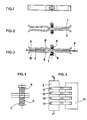
- FIGS 1 to 4 show an embodiment of a contact finger. It can be seen that this: consists of two elastic blades, generally called fishplates, (1) and (2) made of copper or a copper-based alloy of approximately 10 ⁇ 2 mm in cross section, formed so as to be able to elastically pinch a contact bar (3) of approximately 40 x 6 mm in cross-section. Contact between the finger and the operating circuit is ensured in the same way by pinching a strip (4) connected to this circuit. Springs (5) and (6) mounted on the axis (7) ensure the elastic clamping of the assembly with a clamping force of approximately 1 kg.
- the curvature of the fishplates in the area (8) and (9) is such that, practically, the contact bars / fishplates is located at the end of these in (9) and (10).
- Figure 5 shows the test device schematically.
- the aluminum bar (10) of 40 x 6 mm section is fixed at its two ends in the jaws of an alternating traction / compression machine, not shown. In this way, the bar is subjected to alternating forces along the XY axis with a frequency of 155 Hertz. These efforts are reflected at the contact level by alternative micro-slippages comparable to those which occur in electrical installations.
- the compression tensile stress applied to the bar is + 80 MPa.
- the first five pairs which correspond to the techniques practiced in the usual way for the realization of contacts by skewering relate to contacts comprising a bar in AGS / L covered by electrolytic deposition of a layer of tin. 17 ⁇ m thick on under layer bronze.
- the copper fingers are either bare or covered with tin or nickel, or a tin-nickel alloy, or silver.
- the five other pairs which implement the method according to the invention comprise an AGS / L bar covered with 15 ⁇ m of nickel, as described in the example and a second series of 5 copper fingers identical to the first series .
- Each of the ten pairs thus defined has been tested 4 times, that is to say that four identical fingers have been used for each couple in contact with sections of AGS / L bars coated either with nickel or tin and the value of the result was determined by measuring the area of the oxidation spots formed on the surface of the bars after 200,000 cycles.
- Each of these fingers is connected at its other end with contact bars (19) and (20) which are connected to a source of direct current not shown.
- each of the fishplates such as (21) and (22) and the bar (18) is ensured by means of silver contact pads (23) and (24) whose flat and parallel bearing faces have the shape of a square 3 x 3 mm on the side.
- One of the faces of each of these pads is brazed to the splint and the other is in abutment on the surface of the bar section.
- the thickness of these pads is approximately 1 mm and the clamping pressure of the splices of the order of 1 kg. ensures good contact between each pellet and the silver surface of the bar on which it comes to rest.
- the distance D between the fingers (16) and (17) at their contact with the bar (18) via the silver pellets is 50 mm between axes.
- a recording voltmeter (V) is connected to the ends of the fishplates at the contact pads.
- I1 makes it possible to measure the evolution of the voltage as a function of time.
- the intensity of the direct current is fixed once and for all at a constant value of 25 amperes.
- 'R overall electrical resistance
- AGS / L plates of 64 x 72 x 2 mm were also coated with a 15 ⁇ m layer of nickel according to the method described in the example. These plates were then heated locally to a temperature close to the melting point of aluminum in 6 to 7 min. We have managed to obtain on each wafer, on a surface of the order of 1 or 2 cm 2 , an initial melting of the aluminum. After cooling, it was observed that the nickel layer had retained all of its adhesion properties.
- the bars thus coated with nickel are liable to undergo brazing treatments at relatively high temperature, without detachment of the nickel layer.
- This brazing alloy has a melting point of between 340 ° and 395 ° C.
- the nickel layer which, according to the invention, covers an aluminum substrate, a thin layer of silver.
- a deposition will be carried out for example by electrolysis in a silver cyanide bath; as mentioned above.
- Tests have been carried out to study the abrasion behavior of electrical contacts, one of the two contact elements of which is made of aluminum coated with nickel and then silver, the other element being a copper finger, comprising pellets of silver contact brazed at the ends of the fishplates, identical to that shown in Figure 7.
- This finger is plugged in as in the case which has just been described on a section of AGS / L bar 40 x 6 mm in section, covered of 15 ⁇ m of nickel plus 3 ⁇ m of silver as described above.
- a known device makes it possible to subject the section of bar at the frequency of 3,600 cycles / h of alternating displacements in its plane, of approximately 6 mm of amplitude, the finger and, consequently, the silver contact pads remaining fixed. .
- the contact surface of these pellets with the bar is the same as in the previous example, 9 mm2 each.
- the clamping force of the two fishplates against each other is also the same, i.e. 1 kg.
- a series of contact wear tests was performed. During each of these tests, the bar / finger contact underwent 15 to 20,000 cycles.
- Table II below shows the total mass losses in mmg resulting from the wear of the contacts between the bar and the finger. The voltage drop at these contacts is also given. It was measured between the ends of the fishplates at the contact pads and the bar in the immediate vicinity of the contact area.
- This deposit of silver therefore makes it possible to combine the remarkable qualities of a layer of nickel with high adhesion deposited directly on an aluminum substrate with the well-known qualities of silver for making electrical contacts.
- the two contact elements of which are made of aluminum coated with nickel by the method according to the invention. It is also possible to coat at least one of the aluminum contact elements with a layer of silver deposited on a layer of nickel.
- devices according to the invention comprising contact parts made of nickel-plated aluminum on which a contact plate made of copper, or silver, or a contact alloy or pseudo-alloy, resistant to the impact of short-lived electric arcs and also abrasion. It is then possible to use such devices for establishing and breaking under load of circuits, and also for sliding contacts such as those made on manifolds and rings.
Landscapes
- Chemical & Material Sciences (AREA)
- Engineering & Computer Science (AREA)
- Composite Materials (AREA)
- Materials Engineering (AREA)
- Contacts (AREA)
- Manufacture Of Switches (AREA)
- Electroplating Methods And Accessories (AREA)
Applications Claiming Priority (2)
| Application Number | Priority Date | Filing Date | Title |
|---|---|---|---|
| FR7810333 | 1978-03-31 | ||
| FR7810333A FR2421452A1 (fr) | 1978-03-31 | 1978-03-31 | Nouvelle methode de realisation de contacts electriques sur pieces en aluminium |
Publications (3)
| Publication Number | Publication Date |
|---|---|
| EP0004824A2 true EP0004824A2 (de) | 1979-10-17 |
| EP0004824A3 EP0004824A3 (en) | 1979-10-31 |
| EP0004824B1 EP0004824B1 (de) | 1983-03-02 |
Family
ID=9206825
Family Applications (1)
| Application Number | Title | Priority Date | Filing Date |
|---|---|---|---|
| EP79420015A Expired EP0004824B1 (de) | 1978-03-31 | 1979-03-26 | Messerkontakt und Verfahren zum Aufbringen einer Nickelschicht auf ein Aluminiumstück |
Country Status (12)
| Country | Link |
|---|---|
| US (2) | US4360411A (de) |
| EP (1) | EP0004824B1 (de) |
| JP (1) | JPS5510789A (de) |
| BE (1) | BE875216A (de) |
| CA (1) | CA1132639A (de) |
| CH (1) | CH630742A5 (de) |
| DE (1) | DE2964941D1 (de) |
| ES (2) | ES478979A1 (de) |
| FR (1) | FR2421452A1 (de) |
| GR (1) | GR64859B (de) |
| IN (1) | IN151340B (de) |
| IT (1) | IT1113210B (de) |
Families Citing this family (11)
| Publication number | Priority date | Publication date | Assignee | Title |
|---|---|---|---|---|
| JPS59205079A (ja) * | 1983-05-04 | 1984-11-20 | Toyo Kako Kk | 樹脂製バルブ及びその製造方法 |
| ATE38741T1 (de) * | 1984-05-18 | 1988-12-15 | Sprecher Energie Ag | Vakuumschalter. |
| JPH0528067Y2 (de) * | 1984-12-29 | 1993-07-19 | ||
| JP2531752Y2 (ja) * | 1991-10-29 | 1997-04-09 | 株式会社サクラクレパス | 塗布具 |
| US5601695A (en) * | 1995-06-07 | 1997-02-11 | Atotech U.S.A., Inc. | Etchant for aluminum alloys |
| US5703757A (en) * | 1996-01-31 | 1997-12-30 | Alcoa Fujikura Limited | Electronic vehicular junction box having reduced size and weight |
| CA2304360C (en) * | 2000-03-20 | 2009-06-30 | S&C Electric Company | Contact arrangement for electrical power distribution switch or the like |
| JP4593013B2 (ja) * | 2001-06-04 | 2010-12-08 | 古河電気工業株式会社 | アルミニウム合金導電体 |
| FI113912B (fi) * | 2001-12-13 | 2004-06-30 | Outokumpu Oy | Lisäaineellisella pinnoitteella varustettu yhdysterminaali |
| US7137751B2 (en) * | 2003-03-14 | 2006-11-21 | Societe Bic S.A. | Writing instrument with cushioning element |
| US9154008B2 (en) * | 2012-10-02 | 2015-10-06 | Siemens Industry, Inc. | Hybrid rotor bar assemblies, electric motors including hybrid rotor bar assemblies, and methods of assemblying same |
Family Cites Families (18)
| Publication number | Priority date | Publication date | Assignee | Title |
|---|---|---|---|---|
| CA520363A (en) * | 1956-01-03 | A. Payette Joseph | Electrical contact | |
| US1144000A (en) * | 1914-01-19 | 1915-06-22 | Aluminum Francais Soc D | Treament of surfaces of aluminum or alloys of aluminum in order to prepare them for receiving a metallic deposit. |
| GB438228A (en) * | 1934-08-25 | 1935-11-13 | London Aluminium Company Ltd | A new or improved process for the plating of aluminium |
| US2171546A (en) * | 1938-05-03 | 1939-09-05 | Aluminum Co Of America | Surface preparation |
| FR910536A (fr) * | 1944-04-24 | 1946-06-11 | Galvanostegie Almeta Sa De | Procédé pour le recouvrement de la surface d'un objet en aluminium ou en alliage d'aluminium, par un revêtement métallique adhérent |
| US2746136A (en) * | 1951-08-01 | 1956-05-22 | Pechiney Prod Chimiques Sa | Treatment of aluminum and its alloys prior to electro-plating with lead |
| NL6412706A (de) * | 1964-11-02 | 1966-05-03 | ||
| US3472742A (en) * | 1966-03-15 | 1969-10-14 | Webb James E | Plating nickel on aluminum castings |
| US3497655A (en) * | 1968-01-10 | 1970-02-24 | Motorola Inc | Clad metal contacts for reed switches |
| US3666529A (en) * | 1969-04-02 | 1972-05-30 | Atomic Energy Commission | Method of conditioning aluminous surfaces for the reception of electroless nickel plating |
| US3562467A (en) * | 1969-06-04 | 1971-02-09 | Engelhard Min & Chem | Electrical contact |
| US3667991A (en) * | 1970-02-02 | 1972-06-06 | Texas Instruments Inc | Processes for nickel plating metals |
| US3726771A (en) * | 1970-11-23 | 1973-04-10 | Stauffer Chemical Co | Process for chemical nickel plating of aluminum and its alloys |
| BE791008A (fr) * | 1971-11-09 | 1973-05-07 | Citroen Sa | Perfectionnements apportes aux procedes pour la formation sur une paroiexposee a des forces de friction et appartenant a une pieceen alliage leger, d'une revetement metallique composite resistant a l'usure |
| BE788470A (fr) * | 1971-11-12 | 1973-01-02 | Buckbee Mears Co | Procede ameliore d'accroissement de la rigidite des ecrans d'impressio |
| JPS5143098B2 (de) * | 1972-06-19 | 1976-11-19 | ||
| DE2337171A1 (de) * | 1973-07-21 | 1975-04-03 | Bbc Brown Boveri & Cie | Kontaktstueck auf aluminium-guss-basis |
| US4122215A (en) * | 1976-12-27 | 1978-10-24 | Bell Telephone Laboratories, Incorporated | Electroless deposition of nickel on a masked aluminum surface |
-
1978
- 1978-03-31 FR FR7810333A patent/FR2421452A1/fr active Granted
-
1979
- 1979-03-12 IN IN169/DEL/79A patent/IN151340B/en unknown
- 1979-03-23 CH CH272779A patent/CH630742A5/fr not_active IP Right Cessation
- 1979-03-26 EP EP79420015A patent/EP0004824B1/de not_active Expired
- 1979-03-26 DE DE7979420015T patent/DE2964941D1/de not_active Expired
- 1979-03-27 GR GR58703A patent/GR64859B/el unknown
- 1979-03-27 ES ES478979A patent/ES478979A1/es not_active Expired
- 1979-03-28 IT IT21390/79A patent/IT1113210B/it active
- 1979-03-30 BE BE0/194313A patent/BE875216A/xx not_active IP Right Cessation
- 1979-03-30 CA CA324,713A patent/CA1132639A/fr not_active Expired
- 1979-03-30 JP JP3827779A patent/JPS5510789A/ja active Granted
- 1979-07-26 ES ES482845A patent/ES482845A1/es not_active Expired
-
1980
- 1980-08-19 US US06/179,434 patent/US4360411A/en not_active Expired - Lifetime
-
1981
- 1981-01-07 US US06/222,975 patent/US4408110A/en not_active Expired - Fee Related
Also Published As
| Publication number | Publication date |
|---|---|
| GR64859B (en) | 1980-06-05 |
| CH630742A5 (fr) | 1982-06-30 |
| IT1113210B (it) | 1986-01-20 |
| IT7921390A0 (it) | 1979-03-28 |
| JPS5729803B2 (de) | 1982-06-24 |
| CA1132639A (fr) | 1982-09-28 |
| ES478979A1 (es) | 1979-11-16 |
| IN151340B (de) | 1983-04-02 |
| EP0004824A3 (en) | 1979-10-31 |
| DE2964941D1 (en) | 1983-04-07 |
| BE875216A (fr) | 1979-10-01 |
| ES482845A1 (es) | 1980-05-16 |
| EP0004824B1 (de) | 1983-03-02 |
| FR2421452A1 (fr) | 1979-10-26 |
| US4408110A (en) | 1983-10-04 |
| US4360411A (en) | 1982-11-23 |
| JPS5510789A (en) | 1980-01-25 |
| FR2421452B1 (de) | 1981-07-24 |
Similar Documents
| Publication | Publication Date | Title |
|---|---|---|
| EP0004824B1 (de) | Messerkontakt und Verfahren zum Aufbringen einer Nickelschicht auf ein Aluminiumstück | |
| RU2151450C1 (ru) | Термоэлектрический модуль и способ его изготовления | |
| EP2593990B1 (de) | Elektrische verbindungsvorrichtung mit verbesserter leitfähigkeit | |
| WO2001007685A2 (fr) | Procede de nickelage en continu d'un conducteur en aluminium et dispositif correspondant | |
| CN103814157B (zh) | 太阳能电池用互连件材料、太阳能电池用互连件及带互连件的太阳能电池单元 | |
| WO1992010010A1 (fr) | Element de contact de connecteur electrique | |
| EP2904615B1 (de) | Pulver und paste zur erhöhung der leitfähigkeit elektrischer verbindungen | |
| JPWO2015147213A1 (ja) | 導電体及び太陽電池用インターコネクター | |
| WO2007147872A2 (fr) | Procédé de réalisation d'un fil d'aluminium recouvert d'une couche de cuivre et fil obtenu | |
| CH646083A5 (en) | Wire electrode for erosive electrical discharge machining | |
| EP1700325B1 (de) | Elektrisches kontaktelement für elektrische mittel- oder hochspanungsgeräte und entsprechendes verfahren und geräte | |
| JP2002042548A (ja) | 電子部品用リード線とその製造方法、そのリード線を用いた電子部品 | |
| EP3109948B1 (de) | Herstellungsverfahren eines elektrischen kontakts, und elektrischer kontakt | |
| FR2745208A1 (fr) | Procede de fabrication d'un fil stratifie de petit diametre et en particulier d'un fil electrode pour usinage par electroerosion et fil electrode obtenu | |
| FR2519201A1 (fr) | Procede de traitement de surfaces d'organes de liaison electrique | |
| JP2020117770A (ja) | コネクタ用端子材及びコネクタ用端子 | |
| FR2460176A1 (fr) | Procede pour assembler des pieces metalliques, par exemple en aluminium et assemblage ainsi obtenu | |
| EP0586300A1 (de) | Elektrischer Kontakt aus Nickel für einen Verbinder, Verbinder und Herstellungsverfahren | |
| FR2743205A1 (fr) | Procede de traitement de la surface d'un conducteur electrique tel qu'une barre appartenant a un jeu de barres et barre susceptible d'etre obtenue suivant ce procede | |
| CH685379A5 (fr) | Fil métallique stratifié et fil-électrode obtenu à partir d'un fil métallique stratifié pour le découpage par décharges électriques érosives. | |
| WO2002005998A1 (fr) | Fil pour electroerosion a couche superficielle optimisee | |
| FR3117904A1 (fr) | Procede de fabrication d’un conducteur electrique, comme une canne de courant, pour un dispositif electrochimique a haute temperature | |
| FR2743973A1 (fr) | Vitrage comportant un reseau chauffant et procede de fabrication d'un tel vitrage | |
| JP2020117769A (ja) | コネクタ用端子材及びコネクタ用端子 | |
| BE493004A (de) |
Legal Events
| Date | Code | Title | Description |
|---|---|---|---|
| PUAI | Public reference made under article 153(3) epc to a published international application that has entered the european phase |
Free format text: ORIGINAL CODE: 0009012 |
|
| PUAL | Search report despatched |
Free format text: ORIGINAL CODE: 0009013 |
|
| AK | Designated contracting states |
Designated state(s): DE GB NL SE |
|
| AK | Designated contracting states |
Designated state(s): DE GB NL SE |
|
| 17P | Request for examination filed | ||
| DET | De: translation of patent claims | ||
| GRAA | (expected) grant |
Free format text: ORIGINAL CODE: 0009210 |
|
| AK | Designated contracting states |
Designated state(s): DE GB NL SE |
|
| REF | Corresponds to: |
Ref document number: 2964941 Country of ref document: DE Date of ref document: 19830407 |
|
| PGFP | Annual fee paid to national office [announced via postgrant information from national office to epo] |
Ref country code: DE Payment date: 19890208 Year of fee payment: 11 |
|
| PGFP | Annual fee paid to national office [announced via postgrant information from national office to epo] |
Ref country code: SE Payment date: 19890209 Year of fee payment: 11 |
|
| PGFP | Annual fee paid to national office [announced via postgrant information from national office to epo] |
Ref country code: GB Payment date: 19890228 Year of fee payment: 11 |
|
| PGFP | Annual fee paid to national office [announced via postgrant information from national office to epo] |
Ref country code: NL Payment date: 19890331 Year of fee payment: 11 |
|
| PG25 | Lapsed in a contracting state [announced via postgrant information from national office to epo] |
Ref country code: GB Effective date: 19900326 |
|
| PG25 | Lapsed in a contracting state [announced via postgrant information from national office to epo] |
Ref country code: SE Effective date: 19900327 |
|
| PG25 | Lapsed in a contracting state [announced via postgrant information from national office to epo] |
Ref country code: NL Effective date: 19901001 |
|
| NLV4 | Nl: lapsed or anulled due to non-payment of the annual fee | ||
| GBPC | Gb: european patent ceased through non-payment of renewal fee | ||
| PG25 | Lapsed in a contracting state [announced via postgrant information from national office to epo] |
Ref country code: DE Effective date: 19901201 |
|
| EUG | Se: european patent has lapsed |
Ref document number: 79420015.4 Effective date: 19910109 |
|
| PLBE | No opposition filed within time limit |
Free format text: ORIGINAL CODE: 0009261 |
|
| STAA | Information on the status of an ep patent application or granted ep patent |
Free format text: STATUS: NO OPPOSITION FILED WITHIN TIME LIMIT |