EP0004870A1 - Filtre transversal comportant des entrées en parallèle - Google Patents
Filtre transversal comportant des entrées en parallèle Download PDFInfo
- Publication number
- EP0004870A1 EP0004870A1 EP79100803A EP79100803A EP0004870A1 EP 0004870 A1 EP0004870 A1 EP 0004870A1 EP 79100803 A EP79100803 A EP 79100803A EP 79100803 A EP79100803 A EP 79100803A EP 0004870 A1 EP0004870 A1 EP 0004870A1
- Authority
- EP
- European Patent Office
- Prior art keywords
- input
- evaluation
- shift register
- gate
- input signal
- Prior art date
- Legal status (The legal status is an assumption and is not a legal conclusion. Google has not performed a legal analysis and makes no representation as to the accuracy of the status listed.)
- Granted
Links
Images




Classifications
-
- H—ELECTRICITY
- H03—ELECTRONIC CIRCUITRY
- H03H—IMPEDANCE NETWORKS, e.g. RESONANT CIRCUITS; RESONATORS
- H03H15/00—Transversal filters
- H03H15/02—Transversal filters using analogue shift registers
- H03H15/023—Transversal filters using analogue shift registers with parallel-input configuration
-
- H—ELECTRICITY
- H10—SEMICONDUCTOR DEVICES; ELECTRIC SOLID-STATE DEVICES NOT OTHERWISE PROVIDED FOR
- H10D—INORGANIC ELECTRIC SEMICONDUCTOR DEVICES
- H10D44/00—Charge transfer devices
- H10D44/40—Charge-coupled devices [CCD]
- H10D44/45—Charge-coupled devices [CCD] having field effect produced by insulated gate electrodes
- H10D44/452—Input structures
Definitions
- the invention relates to a transversal filter, in which the stages of an analog CTD shift register integrated on a doped semiconductor substrate are provided with parallel inputs and evaluation circuits associated therewith, in which the evaluation circuits each have a region doped opposite to the substrate, a first and a second input gate and have a transfer gate, the transfer gate being arranged directly next to the transfer channel of the CTD shift register, the one input gate having an input signal, the other input gate having a constant DC voltage, the oppositely doped region being connected to a first and the transfer gate having a second clock voltage , and in which the output signal can be tapped at an output of the CTD shift register.
- Transversal filters of this type also form the subject of the German patent application P 26 43 704.7.
- Transverse filter in which a CCD shift register has a plurality of transfer channels isolated from one another by separating diffusions, each of which is individually assigned to the parallel inputs.
- the transfer gate provided in the evaluation circuits consists of the first displacement electrode of the associated transfer channel.
- the transfer channels are brought together in a common output stage, in the area of which the above-mentioned separation diffusions have been omitted.
- the signal components transmitted separately via the channels and arriving with different delays are summed to form an output signal.
- the weighting coefficients with which the signal fed to the parallel inputs is occupied are given by the gate areas in the individual weighting circuits.
- the disadvantage here is that the required semiconductor area increases sharply with the number of parallel inputs.
- a further transversal filter is known from the "Proceedings" mentioned above, printed in the "Japanese Journal of Applied Physics", Vol. 16 (1977), Supplement 16-1, pages 391-396, which differs from the type mentioned at the outset another education of the Be differentiating circuits and the parallel inputs.
- Each individual evaluation circuit here contains two MOS field-effect transistors connected in series and a resistance diffusion, while each parallel input has a stage of a four-phase CCD shift register provided with an input diffusion. The input diffusion is connected to a connection of the resistor and the last shift electrode is arranged adjacent to a shift electrode of a CCD shift register which makes the summation of the signal components.
- the gate of the one MOS field-effect transistor of each evaluation circuit is assigned the input signal, the gate of the other is in each case determined by a DC voltage, ie the size of the current flowing through the transistors and thus the respective evaluation coefficient.
- the transmission properties of the transversal filter can thus be set electrically. It is disadvantageous, however, that the current depends linearly on the DC voltage mentioned only in a small change range.
- the present invention is based on the object of providing a transversal filter of the type mentioned at the outset, the weighting coefficients of which can be set electrically with great accuracy, a large relative setting range being to be covered. This is according to the invention by the in the characterizing part of the patent Claim 1-listed measures achieved.
- the advantage achieved by the invention is, in particular, that the stored digital signals determine in a very clear manner how often an amount of charge given by its area is entered into the associated stage of the CTD shift register from an evaluation circuit, the number depending on the number of the respectively entered quantities of charge result in the evaluation coefficients assigned to the evaluation circuits. Since the charge quantities can be input at a significantly higher frequency than the clocking of the CTD shift register, it is possible to provide large relative setting ranges for the evaluation coefficients, which include, for example, size ratios of 1: 1000 or more. There is a linear dependency between the quantity controlling the setting of an evaluation coefficient, that is to say the stored digital signal, and the set evaluation coefficient. The simple adjustability of the evaluation coefficients, which is provided within wide limits, enables the transversal filter according to the invention to be used in a very versatile manner.
- the transversal filter shown schematically in FIG. 1 is designed as a monolithically integrated semiconductor circuit on a doped semiconductor substrate 1, for example p-type silicon.
- a terminal 2 is supplied with an analog input signal u e , while an analog output signal u a can be tapped at the output 3, the time profile of which corresponds to that of the signal u e after it has passed through a frequency filter with a specific frequency characteristic.
- the frequency characteristic can be that of a low pass, for example.
- a shift register denoted by 4 is designed as a charge-coupled arrangement (CCD) and operates in 3-phase operation. It has a series of electrodes 4 1 1, 412, 413, 422, 423 etc. which are placed close to one another in the direction of displacement R over a thin insulating layer covering the substrate 1, for example a gate oxide layer made of SiO 2 .
- Each three electrodes lying next to each other e.g. 411, 412 and 413 or 42 1 , 422 and 423, belong to a shift register stage, the first electrodes 411, 421 etc. of all stages being connected to a line 5 and connected via this to a shift clock voltage ⁇ 1 while the second electrodes 412, 422 etc. are on a common line 6 connected to a shift clock voltage ⁇ 2 and the third electrodes 413, 423 etc. are connected to a line 7 connected to a shift clock voltage ⁇ 3 .
- each third electrode local maxima of surface potential ⁇ s in the semiconductor substrate 1 So-called potential pots, which are shifted step by step from step to step in the direction of the voltages ⁇ 1 to ⁇ 3 in the direction R. Now one injects electrical charges into these potential pots, each surrounded by space charge zones, which have a polarity that corresponds to that of the minority charge carriers of the substrate 1,
- the output stage AS contains a diffusion region 9 (floating diffusion output) which is temporarily released from external potentials. This is conductively connected to the output 3 via an output amplifier 10.
- the region 9 together with a second diffusion region 11, which is connected via a connection 1 2 to a drain voltage V DD , and a gate electrode 13, which is connected via line 5 to the shift clock voltage ⁇ 1 , represents a field effect transistor which occurs when it occurs of the individual voltage pulses of ⁇ 1 intermittently sets the area 9 to a reference potential.
- the input 2 of the transversal filter is connected to a series of parallel inputs 21, 22, 2n, which are each assigned to individual stages of the shift register 4.
- Leather of these parallel inputs is provided with an evaluation circuit 81, 82, 8n. These each have an area D doped in opposition to the substrate 1 , a first input gate G1, a second input gate G2 and a transfer gate G3, the areas D of all conversion circuits 81 to 8n being formed contiguously and connected to a connection 14, while the transfer gate electrodes G3 all evaluation circuits are also coherent and are provided with a connection 15.
- the first input gate G1 Evaluation circuit 81 is provided with a connection E11, G2 with a connection E12.
- connections E21 and E22 those of the evaluation circuit 8n with En1 and En2.
- the connections E11, E21 and En1 are each connected to the parallel inputs 21, 22 and 2n, while the connections E11 and E21 are connected to a common connection B1 and the connection En2 to a connection B2.
- the evaluation circuit 81 is shown cut along the line II-II.
- the parts already shown in Figure 1 are provided with the same reference numerals.
- the thin insulating layer on which the parts 6 1 , 62, 63 and 411 are placed is denoted by 16.
- the evaluation circuit 81 is set up for a positive evaluation coefficient.
- a constant DC voltage U1 is supplied to the terminal E11 of the first input gate G1 via B1, which is at most as large as the smallest input signal u e to be evaluated, so that a fixed potential threshold W 1 results for the surface potential ⁇ s below G1.
- the input signal u e is fed to the terminal E12 via the parallel input 21, potential values between P 1 (for the maximum signal u e ) and P 0 (for the minimum signal u e ) being obtained below G2.
- an evaluation circuit for example the circuit 8n in FIG. 1, is set up for a negative evaluation coefficient
- the input signal u e is supplied to its first input gate via the connection En1 from a parallel input 2n, while its second input gate is now supplied via a connection En2 and a connection B2 is occupied with a constant DC voltage U2, which is at least as large as the maximum input signal u e to be evaluated and results in a fixed potential value W2 below G2.
- G1 there are potential values P 1 'for the maximum input signal and P C ' for the minimum input signal u e .
- FIG. 4 schematically shows a transversal filter designed according to the invention.
- the shift register 4 can generally consist of one of the known arrangements, known under the term charge transfer devices (CTD, Charge Transfer Device), as described, for example, in the book by Sequin and Tompsett "Charge Transfer Devices” Academic Press, New York , 1975, pages 1 to 18 are described.
- CCD Charge Transfer Device
- Such a charge transfer arrangement can work in 2-phase, 3-phase or 4-phase operation depending on its structure.
- the individual stages of the shift register are shown as blocks in FIG. 4 and are designated 401, 402 to 40n.
- the output stage is again designated AS, while the input stage indicated by 19 in FIG. 1 is omitted because of the better overview.
- the input signal u e supplied via the connection 2 is connected to the parallel inputs 21, 22 to 2n of the shift register 4 and further to the connections E12 and E22 of the evaluation circuits 81 and 82 and to the connection En1 of the evaluation circuits 8n.
- u e is connected to the first input gate G1, while the second input gate G2 is connected to a constant DC voltage U2, which is at least is as large as the largest signal u e . It follows from this that the evaluation circuits 81 and 82 are set up for a positive evaluation coefficient, whereas the circuit 8n is set up for a negative one.
- the evaluation circuits 81, 82 ... 8n are provided with connections 151, 152 ... 15n, to which the clock voltages for the individual transfer gate electrodes G3 are each supplied separately. These clock voltages are derived from a clock voltage Um supplied via a connection TA via a series of AND gates 51, 52 to 5n, the first inputs of which are connected to TA and the outputs of which are connected to connections 151, 152 to 15n. Your second inputs are connected to the outputs of comparators Kol, Ko2 ... Kon. The first inputs of all the comparators Ko1 to Kon are also at the output of a counter Z, the input of which is connected to the terminal TA. The second inputs of the comparators are connected to the outputs of a series of digital memories SP 1 to SPn, the input lines L of which are led to an input K.
- the counter Z Via K and the input line L of the first digital memory SP1, a number in the form of a digital signal is now first entered into it.
- the comparator Ko1 which compares the digital signal stored in SP1 with the output signal of the counter Z, in turn supplies an output signal which opens the AND gate 51 until the counter output signal or the respective counter reading expressed thereby reaches the digital signal in the memory SP1 or exceeds.
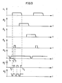
- the clock voltage U T is the terminal 151 of the evaluation circuit 81 from the time t 3 of resetting the counter Z via the open AND gate 51 as long as clock voltage ⁇ G '(Fig.
- the number stored in SP1 which can also have several digits, it can thus be precisely determined how often the amount of charge F, which is proportional to the respective amplitude of u e, is read into stage 401 via input 21.
- the repetition frequency of the voltage ⁇ G 'or' U T must be significantly higher than the repetition frequency of the shift clock voltage ⁇ 1 .
- a frequency divider TE the high repetition rate of U T to the ⁇ for the shift clock voltage 1 required value is lowered, wherein discharged via a flip-flop circuit FF, the voltages ⁇ 1 to ⁇ 3 from the divided clock voltage U T.
- the other digital memories SP2 to SPn can be assigned other digital signals, the numerical values entered blocking the inputs 152 to 15n in the same way via the comparators Ko2 to Kon and the AND gates 52 to 5n as soon as the counter reading the single ones Has reached or exceeded numbers.
- the parallel input 2n is connected to the input En2 of the evaluation circuit 8n and En1 is simultaneously supplied with the constant DC voltage U1, the sign of the evaluation coefficient is also positive for the evaluation circuit 8n.
- each of the evaluation circuits 81, 82 or one of the others can also be set up for negative signs by supplying u e to the respective first gate electrode G1 and simultaneously supplying U2 to the gate electrode G2.
- additional parallel inputs 21 ', 22' to 2n ' are provided which, via assigned evaluation circuits 81', 82 'to 8n', enable charge input at the same stages of the shift register 4 as the parallel inputs 21, 22 to 2n, but in each case on the opposite side of the transfer channel of 4.
- the evaluation circuits 81 to 8n are all aligned for a positive evaluation coefficient, while the evaluation circuits 81 'to 8n' are all aligned for a negative one.
- the sign of the individual evaluation coefficients is electrically programmable. This is done by the fact that the evaluation circuit of one, for example 81 ', of two opposing parallel inputs, for example 21 and 21', is permanently blocked at its one clock voltage input, for example 151 ', which can be done by entering the number "0" in the assigned memory, for example SP1 '. This means that only one of the two opposite parallel inputs is effective and determined by its circuitry the sign of the weighting coefficient assigned to the respective shift register level. In this way, the signs of the evaluation coefficients for the individual stages 401, 402 ... 40n can be selected independently of one another.
- the individual digital memories SP1 to SPn and possibly SP1 'to SPn' consist of the stages of a static shift register, in which the stored information does not have to be regenerated. All numbers to be stored are entered in the order of the stages SP1 ', SP2' one after the other via the input K and the input line L.
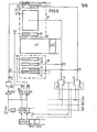
- FIG. 5 schematically shows another exemplary embodiment of the invention, in which the evaluation circuits 81 and 81 'located on the first stage 401 of the shift register on different sides of the transfer channel with the parts D, G1, G2 already described with reference to FIGS. 1 and 4, and G 3 or D ', G1', G2 'and G3' are provided.
- the first input gate electrodes G1 and G1 ' are led to a common connection E11, the second input gate electrodes G2 and G2' to a common connection E12.
- Both evaluation circuits are thus set up for a positive evaluation coefficient when supplying the input signal u from the parallel input 21 to the terminal E12 and with simultaneous supply of U1 to E11, while they have a negative sign when supplying u e to E11 and simultaneous occupancy E12 with the DC voltage U2 surrender.
- SPV1 and SPV2 which can again be designed as stages of the statistical shift register already described with reference to FIG. 4, are reached.
- the output of SPV 1 is connected to gate electrodes of two field effect transistors T1 and T2, the output of SPV2 to the gate electrodes of two further field effect transistors T3 and T4.
- the source-drain path of T2 is between connection 21 and E11, that of T3 between 21 and E 12, that of T1 between B2 and E12 and that of T4 between B1 and E11.
- T3 and T4 are conductive, which leads to the supply of u e to El2 and the supply of U1 on E11 means.
- the circuit 81 is thus designed for a positive evaluation coefficient, which also applies to the circuit 81 '. If a "1" is stored in SPV1, but a "0" in SPV2, u e is connected to connection E11 and U2 to connection E12. A negative sign of the evaluation coefficients of the circuits 81 and 81 'is thus achieved.
- the supply of the clock voltages ⁇ G 'and ⁇ G "provided for the transfer gate electrodes G3 of the circuits 81 and 81' at the inputs 151 and 151 ' is carried out in the manner already described with reference to FIG. 4 via AND gates 51 and 51', comparators Ko1 and Kol ', digital memories SP1 and SP1' and a counter Z controls, the counter Z and the first inputs of the AND gates 51 and 51 'are again connected to a terminal TA, at which a clock voltage U T is obtained. From the voltage U T is also used to derive the clock voltage ⁇ D 'supplied to the regions D and D' doped opposite to the substrate via an inverter INV1 and a delay element VZ.
- the amounts of charge read in via 81 'and 81 are in the ratio of the areas of G2' and G2, this ratio preferably being able to assume a value of 10 or 100.
- the number of the amounts of charge read in is determined by the digital numbers stored in S P 1 and SP1 '. The combination of both read-in processes results in a very fast read-in, even with coefficients whose amount is determined by large digital numerical values.
- the exemplary embodiment of the invention shown in FIG. 6 differs from FIG. 5 only in that the common connections E11 and E12 are actuated differently.
- the evaluation circuits 81 and 81 'for a positive evaluation coefficient which is done by supplying u to E12 and U1 to E11, a "1" is stored in SPV1 and a "0" in SPV2, one via the output of SPV1 controlled switching transistor T5 opens and connects the parallel input 21 to the terminal E12.
- a negative coefficient is set if a "0" is stored in SPV1 and a "1" in SPV2.
- a switching transistor T6 controlled via the output of SPV2 opens, the source-drain path of which is connected on the one hand via an inverter In to 21 and on the other hand to E12.
- the inverted input signal u is thus supplied to the terminal E12, while E 11 is assigned U1.
Landscapes
- Solid State Image Pick-Up Elements (AREA)
- Filters That Use Time-Delay Elements (AREA)
Applications Claiming Priority (2)
| Application Number | Priority Date | Filing Date | Title |
|---|---|---|---|
| DE19782814053 DE2814053A1 (de) | 1978-03-31 | 1978-03-31 | Transversalfilter mit paralleleingaengen |
| DE2814053 | 1978-03-31 |
Publications (2)
| Publication Number | Publication Date |
|---|---|
| EP0004870A1 true EP0004870A1 (fr) | 1979-10-31 |
| EP0004870B1 EP0004870B1 (fr) | 1982-02-03 |
Family
ID=6035893
Family Applications (1)
| Application Number | Title | Priority Date | Filing Date |
|---|---|---|---|
| EP79100803A Expired EP0004870B1 (fr) | 1978-03-31 | 1979-03-15 | Filtre transversal comportant des entrées en parallèle |
Country Status (5)
| Country | Link |
|---|---|
| US (1) | US4231002A (fr) |
| EP (1) | EP0004870B1 (fr) |
| JP (1) | JPS54134535A (fr) |
| CA (1) | CA1135872A (fr) |
| DE (1) | DE2814053A1 (fr) |
Families Citing this family (4)
| Publication number | Priority date | Publication date | Assignee | Title |
|---|---|---|---|---|
| DE3104521A1 (de) * | 1981-02-09 | 1982-08-19 | Siemens AG, 1000 Berlin und 8000 München | Ctd-transversalfilter |
| FR2507027A1 (fr) * | 1981-05-27 | 1982-12-03 | Feldmann Michel | Filtres recursifs a dispositif a transfert de charges |
| DE3235744A1 (de) * | 1982-09-27 | 1984-03-29 | Siemens AG, 1000 Berlin und 8000 München | Transversalfilter mit paralleleingaengen |
| US4616334A (en) * | 1984-12-07 | 1986-10-07 | The United States Of America As Represented By The Secretary Of The Air Force | Pipelined programmable charge domain device |
Citations (6)
| Publication number | Priority date | Publication date | Assignee | Title |
|---|---|---|---|---|
| FR2285680A1 (fr) * | 1974-09-17 | 1976-04-16 | Westinghouse Electric Corp | Systeme de traitement de signaux, notamment compose de dispositifs a transfert de charges |
| US4035628A (en) * | 1975-10-24 | 1977-07-12 | Westinghouse Electric Corporation | Analog transversal filtering and correlation with progressive summation of analog signals |
| BE859128A (fr) * | 1976-09-28 | 1978-01-16 | Siemens Ag | Filtre transversal comportant au moins un registre de decalage analogique et procede pour sa mise en oeuvre |
| US4080581A (en) * | 1975-04-30 | 1978-03-21 | Tokyo Shibaura Electric Co., Ltd. | Charge transfer transversal filter |
| BE862285A (fr) * | 1976-12-23 | 1978-04-14 | Siemens Ag | Filtre transversal |
| US4120035A (en) * | 1977-08-16 | 1978-10-10 | International Business Machines Corporation | Electrically reprogrammable transversal filter using charge coupled devices |
Family Cites Families (1)
| Publication number | Priority date | Publication date | Assignee | Title |
|---|---|---|---|---|
| US3979582A (en) * | 1974-09-17 | 1976-09-07 | Westinghouse Electric Corporation | Discrete analog processing system including a matrix of memory elements |
-
1978
- 1978-03-31 DE DE19782814053 patent/DE2814053A1/de not_active Withdrawn
-
1979
- 1979-03-05 US US06/017,242 patent/US4231002A/en not_active Expired - Lifetime
- 1979-03-15 EP EP79100803A patent/EP0004870B1/fr not_active Expired
- 1979-03-29 CA CA000324461A patent/CA1135872A/fr not_active Expired
- 1979-03-30 JP JP3830379A patent/JPS54134535A/ja active Pending
Patent Citations (14)
| Publication number | Priority date | Publication date | Assignee | Title |
|---|---|---|---|---|
| FR2285680A1 (fr) * | 1974-09-17 | 1976-04-16 | Westinghouse Electric Corp | Systeme de traitement de signaux, notamment compose de dispositifs a transfert de charges |
| US4080581A (en) * | 1975-04-30 | 1978-03-21 | Tokyo Shibaura Electric Co., Ltd. | Charge transfer transversal filter |
| US4035628A (en) * | 1975-10-24 | 1977-07-12 | Westinghouse Electric Corporation | Analog transversal filtering and correlation with progressive summation of analog signals |
| DE2644284A1 (de) * | 1976-09-28 | 1978-04-13 | Siemens Ag | Verfahren zum betrieb eines transversalfilters |
| NL7710541A (nl) * | 1976-09-28 | 1978-03-30 | Siemens Ag | Transversaal filter met tenminste een analoog schuifregister en een werkwijze voor het bedrijf ervan. |
| DE2643704A1 (de) * | 1976-09-28 | 1978-03-30 | Siemens Ag | Transversalfilter mit mindestens einem analogen schieberegister und verfahren zu dessen betrieb |
| BE859128A (fr) * | 1976-09-28 | 1978-01-16 | Siemens Ag | Filtre transversal comportant au moins un registre de decalage analogique et procede pour sa mise en oeuvre |
| FR2365917A1 (fr) * | 1976-09-28 | 1978-04-21 | Siemens Ag | Filtre transversal comportant au moins un registre a decalage analogique et procede pour sa mise en oeuvre |
| DE2658524A1 (de) * | 1976-09-28 | 1978-06-29 | Siemens Ag | Transversalfilter mit mindestens einem analogen schieberegister und ein verfahren zu dessen betrieb |
| BE862285A (fr) * | 1976-12-23 | 1978-04-14 | Siemens Ag | Filtre transversal |
| NL7714198A (nl) * | 1976-12-23 | 1978-06-27 | Siemens Ag | Transversaal filter. |
| DE2658525A1 (de) * | 1976-12-23 | 1978-06-29 | Siemens Ag | Transversalfilter |
| FR2375766A1 (fr) * | 1976-12-23 | 1978-07-21 | Siemens Ag | Filtre transversal |
| US4120035A (en) * | 1977-08-16 | 1978-10-10 | International Business Machines Corporation | Electrically reprogrammable transversal filter using charge coupled devices |
Non-Patent Citations (3)
| Title |
|---|
| 3rd INTERNATIONAL CONFERENCE ON CHARGE COUPLED DEVICES, September 1976, University of Edinburgh, Edinburgh, GB, J.E. DILLEY: "A microcomputer controlled adaptive CCD transversal filter", Seiten 269-276. * Figuren 1, 2; Seite 269, Zeile 1 bis Seite 271, letze Zeile * * |
| NHK LABORATORIES NOTE, Serie Nr. 226, Mai 1978, Tokyo, JP, S. OHNISHI: "Application of charge-coupled device for cancellation of TV ghost signals", Seiten 1, 3-9. * Figuren 1, 4, 8; Seite 6, Zeile 1 bis Seite 8, Zeile 4 * * |
| SIEMENS FORSCHUNGS- UND ENTWICKLUNGSBERICHTE, Band 7, Nr. 3, Mai-Juni 1978, Berlin, DE, K. KNAUER: "CCD transversal filters with parallel-in/serial-out configuration", Seiten 138-142. * Das ganze Dokument * * |
Also Published As
| Publication number | Publication date |
|---|---|
| EP0004870B1 (fr) | 1982-02-03 |
| US4231002A (en) | 1980-10-28 |
| DE2814053A1 (de) | 1979-10-11 |
| CA1135872A (fr) | 1982-11-16 |
| JPS54134535A (en) | 1979-10-19 |
Similar Documents
| Publication | Publication Date | Title |
|---|---|---|
| EP0027881B1 (fr) | Dispositif d'analyse d'image bidimensionnelle intégré monolithiquement comportant un montage de soustraction et procédé pour le commander | |
| DE2144235C3 (de) | Verzögerung sanordnung | |
| CH629630A5 (de) | Transversalfilter mit mindestens einem analogen schieberegister und verfahren zu dessen betrieb. | |
| DE1920077C2 (de) | Schaltungsanordnung zum Übertragen von Ladungen | |
| EP0004870B1 (fr) | Filtre transversal comportant des entrées en parallèle | |
| DE2933440C2 (de) | Ladungsübertragungs-Transversalfilter | |
| EP0004563B1 (fr) | Filtre transversal | |
| DE3717922A1 (de) | Als integrierte schaltung ausgebildete schaltereinrichtung | |
| DE2630085C3 (de) | CCD-Transversalfilter | |
| DE2721812A1 (de) | Auswerteschaltung fuer eine ladungsverschiebeanordnung | |
| EP0057751B1 (fr) | Filtre transversal à dispositif à transfert de charges | |
| DE2936704A1 (de) | Monolithisch integrierte schaltung mit einem zweidimensionalen bildsensor | |
| DE2703317A1 (de) | Ladungsgekoppelte korrelatoranordnung | |
| DE2822746C2 (fr) | ||
| DE2936731C2 (fr) | ||
| DE2813972C2 (fr) | ||
| DE2813997C2 (fr) | ||
| DE2813971C2 (de) | Transversalfilter mit Paralleleingängen | |
| DE2830437A1 (de) | Ladungsgekoppeltes filter | |
| DE2813998C2 (de) | Transversalfilter mit Paralleleingängen | |
| DE3736735C2 (fr) | ||
| DE2838037A1 (de) | Monolithisch integrierte ladungsverschiebeanordnung | |
| AT377635B (de) | Ladungsuebertragungsanordnung | |
| DE2838097C2 (fr) | ||
| DE1967141C3 (de) | Integrierte Halbleiter-Ladungsübertragungsvorrichtung |
Legal Events
| Date | Code | Title | Description |
|---|---|---|---|
| PUAI | Public reference made under article 153(3) epc to a published international application that has entered the european phase |
Free format text: ORIGINAL CODE: 0009012 |
|
| AK | Designated contracting states |
Designated state(s): BE FR GB IT NL |
|
| 17P | Request for examination filed | ||
| ITF | It: translation for a ep patent filed | ||
| GRAA | (expected) grant |
Free format text: ORIGINAL CODE: 0009210 |
|
| AK | Designated contracting states |
Designated state(s): BE FR GB IT NL |
|
| PGFP | Annual fee paid to national office [announced via postgrant information from national office to epo] |
Ref country code: FR Payment date: 19820318 Year of fee payment: 4 |
|
| PGFP | Annual fee paid to national office [announced via postgrant information from national office to epo] |
Ref country code: NL Payment date: 19820331 Year of fee payment: 4 |
|
| PGFP | Annual fee paid to national office [announced via postgrant information from national office to epo] |
Ref country code: BE Payment date: 19820630 Year of fee payment: 4 |
|
| PG25 | Lapsed in a contracting state [announced via postgrant information from national office to epo] |
Ref country code: BE Effective date: 19830315 |
|
| PG25 | Lapsed in a contracting state [announced via postgrant information from national office to epo] |
Ref country code: NL Effective date: 19831001 |
|
| GBPC | Gb: european patent ceased through non-payment of renewal fee | ||
| NLV4 | Nl: lapsed or anulled due to non-payment of the annual fee | ||
| PG25 | Lapsed in a contracting state [announced via postgrant information from national office to epo] |
Ref country code: FR Free format text: LAPSE BECAUSE OF NON-PAYMENT OF DUE FEES Effective date: 19831130 |
|
| REG | Reference to a national code |
Ref country code: FR Ref legal event code: ST |
|
| PG25 | Lapsed in a contracting state [announced via postgrant information from national office to epo] |
Ref country code: GB Effective date: 19881117 |
|
| PLBE | No opposition filed within time limit |
Free format text: ORIGINAL CODE: 0009261 |
|
| STAA | Information on the status of an ep patent application or granted ep patent |
Free format text: STATUS: NO OPPOSITION FILED WITHIN TIME LIMIT |