EP0009131A1 - Procédé pour la modification in-situ de la composition d'alliages de soudage tendre - Google Patents
Procédé pour la modification in-situ de la composition d'alliages de soudage tendre Download PDFInfo
- Publication number
- EP0009131A1 EP0009131A1 EP79103107A EP79103107A EP0009131A1 EP 0009131 A1 EP0009131 A1 EP 0009131A1 EP 79103107 A EP79103107 A EP 79103107A EP 79103107 A EP79103107 A EP 79103107A EP 0009131 A1 EP0009131 A1 EP 0009131A1
- Authority
- EP
- European Patent Office
- Prior art keywords
- solder
- indium
- flux
- lead
- alloy
- Prior art date
- Legal status (The legal status is an assumption and is not a legal conclusion. Google has not performed a legal analysis and makes no representation as to the accuracy of the status listed.)
- Granted
Links
Images



Classifications
-
- H—ELECTRICITY
- H10—SEMICONDUCTOR DEVICES; ELECTRIC SOLID-STATE DEVICES NOT OTHERWISE PROVIDED FOR
- H10W—GENERIC PACKAGES, INTERCONNECTIONS, CONNECTORS OR OTHER CONSTRUCTIONAL DETAILS OF DEVICES COVERED BY CLASS H10
- H10W72/00—Interconnections or connectors in packages
- H10W72/20—Bump connectors, e.g. solder bumps or copper pillars; Dummy bumps; Thermal bumps
-
- B—PERFORMING OPERATIONS; TRANSPORTING
- B23—MACHINE TOOLS; METAL-WORKING NOT OTHERWISE PROVIDED FOR
- B23K—SOLDERING OR UNSOLDERING; WELDING; CLADDING OR PLATING BY SOLDERING OR WELDING; CUTTING BY APPLYING HEAT LOCALLY, e.g. FLAME CUTTING; WORKING BY LASER BEAM
- B23K35/00—Rods, electrodes, materials, or media, for use in soldering, welding, or cutting
- B23K35/22—Rods, electrodes, materials, or media, for use in soldering, welding, or cutting characterised by the composition or nature of the material
- B23K35/24—Selection of soldering or welding materials proper
- B23K35/26—Selection of soldering or welding materials proper with the principal constituent melting at less than 400°C
- B23K35/268—Pb as the principal constituent
-
- B—PERFORMING OPERATIONS; TRANSPORTING
- B23—MACHINE TOOLS; METAL-WORKING NOT OTHERWISE PROVIDED FOR
- B23K—SOLDERING OR UNSOLDERING; WELDING; CLADDING OR PLATING BY SOLDERING OR WELDING; CUTTING BY APPLYING HEAT LOCALLY, e.g. FLAME CUTTING; WORKING BY LASER BEAM
- B23K35/00—Rods, electrodes, materials, or media, for use in soldering, welding, or cutting
- B23K35/22—Rods, electrodes, materials, or media, for use in soldering, welding, or cutting characterised by the composition or nature of the material
- B23K35/36—Selection of non-metallic compositions, e.g. coatings or fluxes; Selection of soldering or welding materials, conjoint with selection of non-metallic compositions, both selections being of interest
- B23K35/3612—Selection of non-metallic compositions, e.g. coatings or fluxes; Selection of soldering or welding materials, conjoint with selection of non-metallic compositions, both selections being of interest with organic compounds as principal constituents
- B23K35/3618—Carboxylic acids or salts
-
- H—ELECTRICITY
- H05—ELECTRIC TECHNIQUES NOT OTHERWISE PROVIDED FOR
- H05K—PRINTED CIRCUITS; CASINGS OR CONSTRUCTIONAL DETAILS OF ELECTRIC APPARATUS; MANUFACTURE OF ASSEMBLAGES OF ELECTRICAL COMPONENTS
- H05K3/00—Apparatus or processes for manufacturing printed circuits
- H05K3/30—Assembling printed circuits with electric components, e.g. with resistors
- H05K3/32—Assembling printed circuits with electric components, e.g. with resistors electrically connecting electric components or wires to printed circuits
- H05K3/34—Assembling printed circuits with electric components, e.g. with resistors electrically connecting electric components or wires to printed circuits by soldering
- H05K3/346—Solder materials or compositions specially adapted therefor
-
- H—ELECTRICITY
- H05—ELECTRIC TECHNIQUES NOT OTHERWISE PROVIDED FOR
- H05K—PRINTED CIRCUITS; CASINGS OR CONSTRUCTIONAL DETAILS OF ELECTRIC APPARATUS; MANUFACTURE OF ASSEMBLAGES OF ELECTRICAL COMPONENTS
- H05K3/00—Apparatus or processes for manufacturing printed circuits
- H05K3/30—Assembling printed circuits with electric components, e.g. with resistors
- H05K3/32—Assembling printed circuits with electric components, e.g. with resistors electrically connecting electric components or wires to printed circuits
- H05K3/34—Assembling printed circuits with electric components, e.g. with resistors electrically connecting electric components or wires to printed circuits by soldering
- H05K3/3489—Composition of fluxes; Application thereof; Other processes of activating the contact surfaces
-
- H—ELECTRICITY
- H10—SEMICONDUCTOR DEVICES; ELECTRIC SOLID-STATE DEVICES NOT OTHERWISE PROVIDED FOR
- H10W—GENERIC PACKAGES, INTERCONNECTIONS, CONNECTORS OR OTHER CONSTRUCTIONAL DETAILS OF DEVICES COVERED BY CLASS H10
- H10W72/00—Interconnections or connectors in packages
- H10W72/071—Connecting or disconnecting
- H10W72/072—Connecting or disconnecting of bump connectors
- H10W72/07251—Connecting or disconnecting of bump connectors characterised by changes in properties of the bump connectors during connecting
-
- H—ELECTRICITY
- H10—SEMICONDUCTOR DEVICES; ELECTRIC SOLID-STATE DEVICES NOT OTHERWISE PROVIDED FOR
- H10W—GENERIC PACKAGES, INTERCONNECTIONS, CONNECTORS OR OTHER CONSTRUCTIONAL DETAILS OF DEVICES COVERED BY CLASS H10
- H10W72/00—Interconnections or connectors in packages
- H10W72/20—Bump connectors, e.g. solder bumps or copper pillars; Dummy bumps; Thermal bumps
- H10W72/251—Materials
-
- H—ELECTRICITY
- H10—SEMICONDUCTOR DEVICES; ELECTRIC SOLID-STATE DEVICES NOT OTHERWISE PROVIDED FOR
- H10W—GENERIC PACKAGES, INTERCONNECTIONS, CONNECTORS OR OTHER CONSTRUCTIONAL DETAILS OF DEVICES COVERED BY CLASS H10
- H10W72/00—Interconnections or connectors in packages
- H10W72/20—Bump connectors, e.g. solder bumps or copper pillars; Dummy bumps; Thermal bumps
- H10W72/251—Materials
- H10W72/255—Materials of outermost layers of multilayered bumps, e.g. material of a coating
-
- H—ELECTRICITY
- H10—SEMICONDUCTOR DEVICES; ELECTRIC SOLID-STATE DEVICES NOT OTHERWISE PROVIDED FOR
- H10W—GENERIC PACKAGES, INTERCONNECTIONS, CONNECTORS OR OTHER CONSTRUCTIONAL DETAILS OF DEVICES COVERED BY CLASS H10
- H10W72/00—Interconnections or connectors in packages
- H10W72/90—Bond pads, in general
- H10W72/921—Structures or relative sizes of bond pads
- H10W72/923—Bond pads having multiple stacked layers
-
- H—ELECTRICITY
- H10—SEMICONDUCTOR DEVICES; ELECTRIC SOLID-STATE DEVICES NOT OTHERWISE PROVIDED FOR
- H10W—GENERIC PACKAGES, INTERCONNECTIONS, CONNECTORS OR OTHER CONSTRUCTIONAL DETAILS OF DEVICES COVERED BY CLASS H10
- H10W72/00—Interconnections or connectors in packages
- H10W72/90—Bond pads, in general
- H10W72/951—Materials of bond pads
- H10W72/952—Materials of bond pads comprising metals or metalloids, e.g. PbSn, Ag or Cu
Definitions
- the invention relates to a method for in situ modification 'of the compositions of solder alloy containing lead and a wetting agent, such as tin or indium. With this method, the lead content in the alloy of the soldered connection is increased, which is particularly important in semiconductor production.
- solder connections are obtained, for example, with lead alloys such as 95: 5 lead / tin or 95: 5 lead / indium.
- solder connections made of pure lead or lead with a high lead content would, however, exhibit 2 to 3 times better fatigue behavior compared to conventional solder alloys. Also, solder connections made of essentially pure lead would have an increased creep resistance under permanent load compared to that of a 50:50 lead / indium solder.
- the object of the invention is therefore to provide a method for changing the compositions of solder alloys containing lead and a wetting agent in situ.
- the object of the invention is achieved by a method of the type mentioned at the outset, which is characterized in that. that the molten solder alloy is heated with a solder flux for a sufficient time to reduce the level of wetting agent in the molten solder alloy.
- soldered joints with increased resistance to fatigue and also with increased creep resistance can be obtained compared to previously known soldering alloys.
- the composition of the solder alloy can be changed after the connection point has been produced by the action of a suitable soldering flux, for example the lead content of the solder connections can be increased to a desired value.
- solder connections made from a lead alloy can be increased by modifying them, in particular in a method in which the integrated semiconductor chips are turned onto the substrates before soldering and then soldered on.
- Conventional solders for example 95: 5 lead / tin and 95: 5 lead / indium or 50:50 lead / indium solders, are used to form solder connections of this type, and then the excess tin or indium from the resulting connections is fluxed, which contains at least one resin acid selected from the group of monocarboxylic acids of an alkylated hydrophenanthrene skeleton with the empirical formula C19H20COOH.
- the flux reduces the tin content of a 95: 5 lead / tin solder joint to less than 1% by weight at elevated temperatures. Indium reacts even more easily and can be leached out even more easily from a lead / indium solder connection.
- semiconductor chips 1 are used, which are referred to below as integrated semiconductor chips (FIG. 1) and consist of a first aluminum metallization 2, a silicon dioxide layer 3 and a contact point 4, the latter consisting of a 200 nm thick chromium layer 5, one 1000 nm thick copper layer 6 with an initial, about 80 nm thick layer of a chrome copper phase and a 140 nm thick gold layer 8 is formed.
- Each integrated semiconductor chip contains 121 such contact points 4.
- Wafers which contain integrated semiconductor chips of this type are referred to below as integrated semiconductor wafers, each wafer containing some 100 integrated semiconductor chips.
- the solder connection point 9 was evaporated onto the contact points 4 at a height of 0.1143 mm through a mask. Because of the higher vapor pressure of lead, it is first evaporated in a layer 10, and then the indium is evaporated in a layer 11. The shape of the evaporated solder connection points was that of a truncated cone.
- Subsequent wetting which is used here, denotes melting for modifying the solder connection points, for example in order to fuse the two layers of the solder connection point 4 together and thereby incorporate the wetting agent, the indium / or tin layer 11, the lead as a solder alloy.
- compositions of the solder alloys were determined by measuring their melting points using a Perkin-Elmer differential calorimeter (DSC). Because experimentally easier to carry out, the cooling curves were used in the measurements. Standards were made from known compositions and tested under the same conditions as the solder alloys and the solder joints using the same amounts of material.
- the fluxes used were from Alpha Metals, for example a-102-1500 with an addition of 20% isopropyl alcohol (IPA) by weight of. a- 102-1500, and a-100-40.
- IPA isopropyl alcohol
- TBC water-white rosin and a water-soluble flux called TBC, which consisted of 50% by volume of triethanolamine and 50% by volume of butyl glycol (butyl cellosolve), were also used.
- the a-102-1500 flux is referred to below as a-102, with the second half of the number (1500) indicating the viscosity of the flux.
- the a-100-40 flux is referred to below as a-104.
- the a-102 flux is supplied as a 68% by weight solution of abietic acid in benzyl alcohol and the a-104 flux as a 40% by weight solution of abietic acid in isopropanol.
- Rosin is a rosin acid of the monocarboxylic acid type of the alkylated hydrophenanthrene skeleton with an empirical formula C 19 H 29 COOH.
- the remaining half wafer was subjected to the two reflow treatments in reverse order, that is, first a two minute reflow treatment at 275 ° C in a nitrogen atmosphere and then a two minute one Subject to reflow treatment with a-102 flux at 275 ° C.
- the invention also permits the repair or replacement of one or more chips from a plurality of chips connected to a carrier, for example a multilayer ceramic substrate, by a high-melting solder, for example an 85% lead / 15% indium solder (FIG. 2).
- a high-melting solder for example an 85% lead / 15% indium solder (FIG. 2).
- the chip can be mechanically separated or removed from the carrier.
- a new chip is then placed on the vacated area, the chip being provided with a low-melting solder, for example a 55% lead / 45% indium solder, and the unit is brought to a temperature (for example 250 ° C., FIG.
- the water-soluble TBC (triethanolamine / butyl cellosolve) caused only a slight decrease in the indium content of the solder connection points. Chips without contact points had a higher indium content, reflecting the lack of influence from copper and gold metallurgy.
- the indium content which was determined by the weight loss, showed slight fluctuations which were attributed to inadequate cleaning of the samples after the leaching melt.
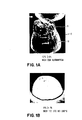
- Figs. 1A and 1B show electron micrographs of two solder pads; one immediately after evaporation and the other half an hour after the leaching melt at 280 ° C in a-102 flux.
- the indium cover 11 is visible on the vapor-deposited solder joint, as is the change in the volume of the solder joint due to the heating in the flux, which reflects the removal of the indium from the solder joint.
- the time dependence of the a-102 and TBC (triethanolamine-butyl cellosolve) reactions was determined at 280 ° C at 50:50 indium / lead solder joints.
- the a-102 flux was reacted at 280 0 with the vapor-deposited on the chips and solder pads with the same according to a first performed melting: A difference between the two could, as can be seen from Table IV, are not detected.
- Fig. 3 the time dependence of the leaching of indium by a-1 0 2 and TBC (triethanolamine / butyl cellosolve) flux is plotted. After a start-up time for the a-102 flux, a very rapid leaching takes place, the speed decreasing as the indium concentration decreases. The amount leached out by the TBC flux decreased at a constant rate.
- Figure 4 shows the time dependence of the leaching of indium by the a-102 flux at different temperatures, the 250 0 curve probably having the same shape as the 280 curve when additional points are measured. Note that the indium content after 5 minutes at 350 ° C is essentially the same as after half an hour at 280 ° C.
- the time in the experiments described above is the total time in the oven. 5 shows the thermal profile of an oven which has been heated to 280.degree. This was obtained by mounting the thermocouple in a flux beaker and determining the temperatures of the beaker placed in the oven. All conditions were similar to the experimental conditions. After 5 minutes The temperature is only 245 ° C, which is the start-up time that is shown in FIGS. 3 and 4 appears to explain ..
- the figures 6A and 6B show intermediate stages in the production of a modified solder connection of a chip 20 to a, conductor pattern 21 on a ceramic carrier 22.
- the integrated semiconductor chip 20, not shown, contains integrated circuits. It is covered with a first aluminum conductor pattern 23, parts of which are exposed via contact openings in the passivating layer 24, for example made of silicon dioxide.
- the contact points 4 (as in FIG. 1) are formed in contact with the underlying metallization 23 over each opening.
- a lead layer 10 and a tin layer 11A are deposited as double-layer solder connection points 9 on each contact point.
- This double-layer solder connection point 9 can be heated in order to fuse the tin layer 11A with the lead layer 10 to form a solder connection point 25 made of a 5:95 tin / lead alloy.
- the chip 20 is then placed relative to the ceramic substrate 22 to make solder connections 25 to the metallization 21 of the ceramic substrate 22 at the desired locations, and the units are bonded together by conventional heating.
- the voids between the chip 20 connected to the substrate 22 are filled with a-102 flux 3 and the assembly is heated at 350 ° C for leaching for 1/2 hour.
- the tin content in the alloy of the solder pads 25 was reduced to about 0.4% tin.
Landscapes
- Engineering & Computer Science (AREA)
- Mechanical Engineering (AREA)
- Electric Connection Of Electric Components To Printed Circuits (AREA)
- Wire Bonding (AREA)
Applications Claiming Priority (2)
| Application Number | Priority Date | Filing Date | Title |
|---|---|---|---|
| US94422478A | 1978-09-20 | 1978-09-20 | |
| US944224 | 1978-09-20 |
Publications (2)
| Publication Number | Publication Date |
|---|---|
| EP0009131A1 true EP0009131A1 (fr) | 1980-04-02 |
| EP0009131B1 EP0009131B1 (fr) | 1981-12-23 |
Family
ID=25481021
Family Applications (1)
| Application Number | Title | Priority Date | Filing Date |
|---|---|---|---|
| EP79103107A Expired EP0009131B1 (fr) | 1978-09-20 | 1979-08-23 | Procédé pour la modification in-situ de la composition d'alliages de soudage tendre |
Country Status (5)
| Country | Link |
|---|---|
| EP (1) | EP0009131B1 (fr) |
| JP (1) | JPS5846176B2 (fr) |
| CA (1) | CA1122856A (fr) |
| DE (1) | DE2961610D1 (fr) |
| IT (1) | IT1122873B (fr) |
Cited By (4)
| Publication number | Priority date | Publication date | Assignee | Title |
|---|---|---|---|---|
| EP0073383A3 (en) * | 1981-09-02 | 1984-08-08 | Hitachi, Ltd. | Semiconductor device having external electrodes bonded to electrodes on a semiconductor substrate and method of fabricating such a semiconductor device |
| EP0068091A3 (en) * | 1981-06-30 | 1984-11-14 | International Business Machines Corporation | Method for connecting a semiconductor chip to a substrate and such connection |
| US4498096A (en) * | 1981-01-30 | 1985-02-05 | Motorola, Inc. | Button rectifier package for non-planar die |
| EP0365768A1 (fr) * | 1988-10-17 | 1990-05-02 | International Business Machines Corporation | Composition de flux et procédé pour diminuer la teneur en étain dans des joints soudés en alliage plomb-étain |
Families Citing this family (2)
| Publication number | Priority date | Publication date | Assignee | Title |
|---|---|---|---|---|
| US5007163A (en) * | 1990-04-18 | 1991-04-16 | International Business Machines Corporation | Non-destructure method of performing electrical burn-in testing of semiconductor chips |
| CN105759522B (zh) * | 2016-05-11 | 2019-01-22 | 深圳市华星光电技术有限公司 | Tft基板的断线修复方法 |
Citations (3)
| Publication number | Priority date | Publication date | Assignee | Title |
|---|---|---|---|---|
| US2043573A (en) * | 1934-05-26 | 1936-06-09 | American Smelting Refining | Process for recovering tin |
| US3380821A (en) * | 1965-10-21 | 1968-04-30 | Gen Motors Corp | Heat treatable creep resistant solder alloy |
| US3478414A (en) * | 1967-05-05 | 1969-11-18 | Ibm | Water white rosin flux in benzyl alcohol solution |
-
1979
- 1979-07-27 CA CA332,645A patent/CA1122856A/fr not_active Expired
- 1979-08-14 JP JP54102850A patent/JPS5846176B2/ja not_active Expired
- 1979-08-23 EP EP79103107A patent/EP0009131B1/fr not_active Expired
- 1979-08-23 DE DE7979103107T patent/DE2961610D1/de not_active Expired
- 1979-08-29 IT IT25326/79A patent/IT1122873B/it active
Patent Citations (3)
| Publication number | Priority date | Publication date | Assignee | Title |
|---|---|---|---|---|
| US2043573A (en) * | 1934-05-26 | 1936-06-09 | American Smelting Refining | Process for recovering tin |
| US3380821A (en) * | 1965-10-21 | 1968-04-30 | Gen Motors Corp | Heat treatable creep resistant solder alloy |
| US3478414A (en) * | 1967-05-05 | 1969-11-18 | Ibm | Water white rosin flux in benzyl alcohol solution |
Non-Patent Citations (1)
| Title |
|---|
| FEINWERKTECHNIK, BAND 76, 1972, Heft 3, Seiten 130-134 Munchen, DE. P.A. AINSWORTH: "Beeinflussung der mechanischen Eigenschaften von Weichlotverbindungen in elektronischen Ausrustungen" * Seiten 130-134 * * |
Cited By (4)
| Publication number | Priority date | Publication date | Assignee | Title |
|---|---|---|---|---|
| US4498096A (en) * | 1981-01-30 | 1985-02-05 | Motorola, Inc. | Button rectifier package for non-planar die |
| EP0068091A3 (en) * | 1981-06-30 | 1984-11-14 | International Business Machines Corporation | Method for connecting a semiconductor chip to a substrate and such connection |
| EP0073383A3 (en) * | 1981-09-02 | 1984-08-08 | Hitachi, Ltd. | Semiconductor device having external electrodes bonded to electrodes on a semiconductor substrate and method of fabricating such a semiconductor device |
| EP0365768A1 (fr) * | 1988-10-17 | 1990-05-02 | International Business Machines Corporation | Composition de flux et procédé pour diminuer la teneur en étain dans des joints soudés en alliage plomb-étain |
Also Published As
| Publication number | Publication date |
|---|---|
| DE2961610D1 (en) | 1982-02-11 |
| JPS5846176B2 (ja) | 1983-10-14 |
| CA1122856A (fr) | 1982-05-04 |
| EP0009131B1 (fr) | 1981-12-23 |
| IT1122873B (it) | 1986-04-30 |
| JPS5574160A (en) | 1980-06-04 |
| IT7925326A0 (it) | 1979-08-29 |
Similar Documents
| Publication | Publication Date | Title |
|---|---|---|
| DE69217617T2 (de) | Verbindungsverfahren unter Verwendung eines aus mehrfach abwechselnden Gold- und Zinnschichten bestehenden Lotes | |
| DE69837224T2 (de) | Mit bleifreiem Lötmittel verbundene elektronische Vorrichtung | |
| DE19823615B4 (de) | Lötflussmittel | |
| DE19545783B4 (de) | Verfahren zur Spezifizierung der Eignung eines organischen Stoffes als Lötflussmittel und Lötverfahren unter Verwendung desselben | |
| DE69900894T2 (de) | Gegen Ermüdung widerstandsfähige, bleifreie Legierung | |
| DE69521762T2 (de) | Bleifreies niedrigschmelzendes Lot mit verbesserten mechanischen Eigenschaften und mit diesem Lot verbundene Gegenstände | |
| DE69522993T2 (de) | Flussmittel und Verfahren zum Weichlöten | |
| DE2424857C2 (de) | Verfahren zur Herstellung einer Lötverbindung durch Aufschmelzlöten | |
| DE69503824T2 (de) | Verfahren von Ternär-C4 Typ bei niedriger Temperatur | |
| DE69813701T2 (de) | Elektrodenstruktur einer Siliziumhalbleiteranordnung | |
| DE60217199T2 (de) | Bleifreies Weichlot und Weichlotverbindung | |
| EP2456589B1 (fr) | Connection sans plomb à haute temperature | |
| DE69022668T2 (de) | Elektronische Verbindungen, Verfahren zur Bildung von Endverbindern dafür und Paste zur Ausbildung derselben. | |
| DE68906853T2 (de) | Flussmittelzusammensetzung und Verfahren zur Herabsetzung des Zinngehalts in Blei-Zinn-Lotverbindungen. | |
| DE60300669T2 (de) | Bleifreie Weichlötlegierung | |
| DE3650544T2 (de) | Bleibasislegierungen und Verwendung zum Herabsetzen der Elektromigrationsaktivität | |
| DE69512898T2 (de) | Hochfeste lötlegierung | |
| EP0009131B1 (fr) | Procédé pour la modification in-situ de la composition d'alliages de soudage tendre | |
| DE19750104B4 (de) | Verwendung einer Lotpaste für Chipkomponenten | |
| DE4016384A1 (de) | Elektronische schaltungseinrichtung | |
| DE60305119T2 (de) | Auslaugbeständige Lötlegierungen für elektrisch leitende Dickfilme auf Silberbasis | |
| DE19542043A1 (de) | Bleifreie Niedertemperaturlegierung und Verfahren zur Bildung einer mechanisch überlegenen Verbindung unter Verwendung dieser Legierung | |
| DE3720594C2 (fr) | ||
| DE1752137B2 (de) | Verfahren zum Löten von mikrominiaturisierten Schaltkreisen und Flußmittel zur Durchführung des Verfahrens | |
| DE3740773A1 (de) | Verfahren zum herstellen elektrisch leitender verbindungen |
Legal Events
| Date | Code | Title | Description |
|---|---|---|---|
| PUAI | Public reference made under article 153(3) epc to a published international application that has entered the european phase |
Free format text: ORIGINAL CODE: 0009012 |
|
| AK | Designated contracting states |
Designated state(s): DE FR GB |
|
| 17P | Request for examination filed | ||
| GRAA | (expected) grant |
Free format text: ORIGINAL CODE: 0009210 |
|
| AK | Designated contracting states |
Designated state(s): DE FR GB |
|
| REF | Corresponds to: |
Ref document number: 2961610 Country of ref document: DE Date of ref document: 19820211 |
|
| PGFP | Annual fee paid to national office [announced via postgrant information from national office to epo] |
Ref country code: DE Payment date: 19890904 Year of fee payment: 11 |
|
| PGFP | Annual fee paid to national office [announced via postgrant information from national office to epo] |
Ref country code: GB Payment date: 19900704 Year of fee payment: 12 |
|
| PG25 | Lapsed in a contracting state [announced via postgrant information from national office to epo] |
Ref country code: DE Effective date: 19910501 |
|
| PGFP | Annual fee paid to national office [announced via postgrant information from national office to epo] |
Ref country code: FR Payment date: 19910726 Year of fee payment: 13 |
|
| PG25 | Lapsed in a contracting state [announced via postgrant information from national office to epo] |
Ref country code: GB Effective date: 19910823 |
|
| GBPC | Gb: european patent ceased through non-payment of renewal fee | ||
| PG25 | Lapsed in a contracting state [announced via postgrant information from national office to epo] |
Ref country code: FR Effective date: 19930430 |
|
| REG | Reference to a national code |
Ref country code: FR Ref legal event code: ST |
|
| PLBE | No opposition filed within time limit |
Free format text: ORIGINAL CODE: 0009261 |
|
| STAA | Information on the status of an ep patent application or granted ep patent |
Free format text: STATUS: NO OPPOSITION FILED WITHIN TIME LIMIT |