EP0009600A2 - Procédé et dispositif d'interface pour exécuter des operations de maintenance sur une interface entre un processeur de maintenance et une pluralité d'unités fonctionnelles à vérifier d'un système de traitement de données - Google Patents
Procédé et dispositif d'interface pour exécuter des operations de maintenance sur une interface entre un processeur de maintenance et une pluralité d'unités fonctionnelles à vérifier d'un système de traitement de données Download PDFInfo
- Publication number
- EP0009600A2 EP0009600A2 EP79103076A EP79103076A EP0009600A2 EP 0009600 A2 EP0009600 A2 EP 0009600A2 EP 79103076 A EP79103076 A EP 79103076A EP 79103076 A EP79103076 A EP 79103076A EP 0009600 A2 EP0009600 A2 EP 0009600A2
- Authority
- EP
- European Patent Office
- Prior art keywords
- data
- interface
- functional unit
- signals
- maintenance processor
- Prior art date
- Legal status (The legal status is an assumption and is not a legal conclusion. Google has not performed a legal analysis and makes no representation as to the accuracy of the status listed.)
- Granted
Links
Images

Classifications
-
- G—PHYSICS
- G06—COMPUTING OR CALCULATING; COUNTING
- G06F—ELECTRIC DIGITAL DATA PROCESSING
- G06F11/00—Error detection; Error correction; Monitoring
- G06F11/22—Detection or location of defective computer hardware by testing during standby operation or during idle time, e.g. start-up testing
- G06F11/2294—Detection or location of defective computer hardware by testing during standby operation or during idle time, e.g. start-up testing by remote test
-
- G—PHYSICS
- G06—COMPUTING OR CALCULATING; COUNTING
- G06F—ELECTRIC DIGITAL DATA PROCESSING
- G06F11/00—Error detection; Error correction; Monitoring
-
- G—PHYSICS
- G06—COMPUTING OR CALCULATING; COUNTING
- G06F—ELECTRIC DIGITAL DATA PROCESSING
- G06F11/00—Error detection; Error correction; Monitoring
- G06F11/07—Responding to the occurrence of a fault, e.g. fault tolerance
- G06F11/16—Error detection or correction of the data by redundancy in hardware
- G06F11/1608—Error detection by comparing the output signals of redundant hardware
- G06F11/1625—Error detection by comparing the output signals of redundant hardware in communications, e.g. transmission, interfaces
Definitions
- the invention relates to an interface between a maintenance processor and a plurality of individually testable functional units of a data processing system for the bidirectional transmission of data and control signals when executing maintenance operations controlled by the maintenance processor and characterized by access to registers and data collection paths in a selected functional unit.
- a maintenance processor which has independent access to the main memory of the data processing system, in which test programs for a test routine can be loaded from a peripheral magnetic tape.
- the maintenance processor is selectively connected to one of several functional units of the data processing system to be checked, such as e.g. B. a processor or a peripheral control unit.
- test programs are read serially from a defined memory area of the main memory and executed by the maintenance processor.
- the test routine continues until the result of an executed command indicates a recognized error and / or such an error is located in the functional unit under test.
- a test operation essentially consists in first setting a defined number of flip-flops in the functional unit to be tested into a specific state, then querying the effective operating state of these flip-flops and comparing them with a predetermined status.
- the interface between the maintenance processor and the functional unit to be tested is designed such that the signals belonging to a test operation or a part thereof can be transmitted in parallel via permanently connected lines.
- a selection matrix is provided at the interface of the maintenance processor, which only leads out selected flip-flops through to the maintenance processor.
- the interface between the maintenance processor and the functional unit to be tested is very broad and must also be adapted to the different properties of the functional unit to be tested.
- a broad and individually designed interface already harbors a critical source of error.
- the hardware expenditure for the test routine becomes very large, the interface itself cannot be standardized, so it cannot be flexibly adapted to different applications.
- a result that can only be used to a limited extent is achieved with a relatively high outlay. It should be borne in mind that in larger data processing systems with a corresponding structure, a large number of such functional units should be able to be tested autonomously and the maintenance interface is counted as "hardcore", i. H. must be functional even in the event of a fault if maintenance tasks are to be carried out.
- each interface connection to a functional unit regardless of its functional scope, is of identical design, via which data signals are bit-serial in both directions, accompanied by clock signals with a secure transmission method and additionally uncoded, and only emergency signals are transmitted, and that in each functional unit as well
- a uniformly designed interface adapter is provided, which serves as a recoder and buffer for control and data information to and from the functional unit, whose internal interface to the functional unit is therefore much wider than the internal interface to the maintenance processor and is adapted to the structure of the parallel data paths in the functional units and which controls the exchange of information via the internal interface with strobe lenses.
- This solution has the advantage that the maintenance interface is not only standardized, that is, uniform for all functional units, but is also kept as narrow as possible. This is based on the fact that information about this interface is transmitted bit-serial in both directions over data lines which are accompanied by direction-dependent clock signals.
- a coded, that is to say secured, transmission method is used which, because of its redundancy, allows all individual errors and most multiple errors to be identified during the transmission itself or the data transfer into the receiving circuits.
- the transmission procedure is designed so that the maintenance processor controls the procedure in any case, so the functional units to be tested only respond to requests.
- the interface is completely transparent with regard to the message length and also the type of information to be transmitted, which provides its flexibility. This also applies in particular to data transmission speed that can vary by orders of magnitude in different functional units. Only a few signals are exchanged uncoded via the interface between the maintenance processor and the functional unit to be tested. Such "emergency signals" cannot be transmitted in coded form, since they may only assume a minimum of functionality of the connected functional unit. These signals, here a request signal from a malfunctioning functional unit to the maintenance processor and a reset signal from the maintenance processor to the functional unit, which permits hard resetting of the essential circuits of this functional unit, are generally defined in the same way for all functional units, so that these two are also separated transmitted signals mean no loss of flexibility of the interface.
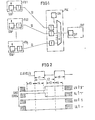
- a Maintenance interface are a number of functional units FU1, FU2 ... FUj of a data processing system indicated schematically.
- the mode of operation and the purpose of the individual functional units of such a data processing system are of no particular importance in the present context. Therefore, it should only be hinted here that units of the data processing system are understood to take over certain functions independently and therefore should also be monitored for their proper functioning by a maintenance processor SVP. Examples of such functional units include only the primary storage system, processing units or input / output units of the data processing system.
- the maintenance interface between these functional units FU1 ... FUj and the maintenance processor SVP is indicated by interface lines SI which are connected via a coordinator circuit PSC to an input / output port SIP of the maintenance processor SVP.
- the coordinator circuit PSC essentially contains an interface multiplexer SIM to which the interface lines SI are connected via transmitter modules T. In the individual functional units, these interface lines SI are likewise terminated by transmitter modules T, and these are connected to an interface adapter SIA.
- This interface adapter a highly integrated component, which will be explained in more detail later, essentially has the task of converting the narrow interface connection SI into a wider interface to the connected functional unit FUj in such a way that the signals transmitted via it can be easily evaluated by the functional unit FU.
- the interface adapter SIA allows the actual interface connection 31 to be kept as narrow as possible. This point of view is not just for reasons of effort essential because e.g. B. very many functional units FUj are to be monitored by the maintenance processor SVP, but also for reasons of availability. For the Thomasstellenansch l ow SI into a functional unit must also be more functional if maintenance tasks are to be performed.
- information is transmitted bit-serial in both directions via data lines which are accompanied by clock signals. Only signals that cannot be transmitted in coded form, that they can only assume a minimum of functionality, are transmitted separately.
- an output clock signal CLO a data output signal DAO and a reset signal RES are output by the maintenance processor via the interface connection SI.
- an input clock signal CLI derived from the output clock signal CLO
- a data input signal DAI a data input signal DAI.
- a request signal SRQ are transmitted from the interface adapter SIA to the maintenance processor SVP.
- the coding can first be taken from the pulse diagrams of these interface signals shown in FIG. 2.
- the output clock signal CLO and the data output signal DAO or the input clock signal CLI and the data input signal DAI work together as clock and data signals of a bit-serial transmission system.
- each information bit is encoded in a sample pair of the data output signal DAO or the data input signal DAI. 2 shows the encodings permitted for the data signals. Two successive leading edges of the clock signals determine each CLO or CLI the evaluation times for the associated data signals DAO or DAI.
- a low level L with a subsequent high level H in the data signal DAO or DAI means the state " ⁇ " of the information bit, the reverse case defines the state "1".
- a third combination with high level H without a signal change corresponds to a special character S, the fourth possible combination with low level L without a change of state is prohibited.
- the redundancy contained in this coding is used to detect transmission errors via the interface connection SI.
- the receiving circuits in the respective interface adapter SIA or the maintenance processor SVP are designed so that one element of these data signals is evaluated with two successive leading edges of the " clock signals CLO or CLI.
- the following time conditions apply:
- the clock signals must not have a certain, technologically determined maximum frequency
- the state of a data signal DAO or DAI must not change shortly before or after the evaluation time due to the finite decision-making power of the evaluation circuits.
- the corresponding times t3 and t4 for the lead or lag in the data signal are indicated in Fig. 2.
- the transmission method may be as slow as desired below this maximum frequency.
- the timing of the reception circuits is only controlled by the accompanying clock signals CLO or CLI and does not itself require any time-determining elements. This means that the transmission process is flexible on functional units with different properties, controlled by maintenance processor SVP, customizable.
- the header sequence KS which consists of two information elements, represents a coding for the mailing type.
- the header sequence KS contains z. B. in a command transmission two information bits in the state "1” and in a data or empty frame transmission two information bits in the state "0 ⁇ ".
- the length of the text TX is fundamentally variable, but it only contains information elements "0 ⁇ " for an empty frame transmission. Because of the variable length of the text part, the end sequence ES serves to mark the end of the program and consists of two successive special characters "S" and a concluding information element "1".
- Command broadcasts CMD are used to transmit maintenance commands from the maintenance processor SVP to the corresponding functional unit FUj or to the interface adapter SIA assigned to this functional unit. Therefore, they always start from the maintenance processor SVP and are evaluated in the corresponding interface adapter SIA, at the same time, but sent back to the maintenance processor SVP together with the input clock signal CLI as data input signals DAI for control purposes.
- Such a command transmission can be followed by data transmissions DTS, with which the maintenance processor SVP transmits data to a functional unit FUj.
- data transmissions DTS are also evaluated by the assigned interface adapter SIA and, at the same time, unchanged for control purposes sent back to the maintenance processor SVP in the same way as the command was sent.
- An empty frame transmission BLK offers the assigned interface adapter SIA the possibility to easily generate a data transmission to the maintenance processor SVP. If the interface adapter SIA receives such an empty frame transmission BLK from the maintenance processor, the header and end sequences KS and ES remain unchanged. Instead of the information elements "0 ⁇ " in the text part, the interface adapter SIA now uses data offered by the functional unit FUj with the corresponding pairwise encryption.
- the interface connection SI only requires three lines for the transmission of the clock signals CLO or CLI, the data signals DAP or DAI and the reset signal RES or the request signal SRQ.
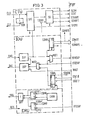
- FIG. 3 A block diagram of such an interface adapter SIA, which can be implemented as an LSI circuit, is shown in FIG. 3. This block diagram is divided into three parts, a time control unit CTO, an input / output unit IOU and an error detection unit ERU.
- the timing control unit CTU receives the output clock signal CLO from the maintenance processor SVP and converts it into the input clock signal CLI in a first NOR gate NOR1.
- the output clock signal CLO of the maintenance processor SVP is supplied in the time control unit CTU to a set of status flip-flops SFF, which is only indicated schematically in FIG. 3.
- SFF state flip-flops SFF initially include two clock flip-flops TP1 and TP2, not shown in detail, whose function is briefly summarized in Table 1:
- clock flip-flops TP1 or TP2 are clocked with the rising or falling edge of the output clock signal CLO, have a D input to which the specified set signal is fed and are hard reset by the reset signal RES of the maintenance processor SVP.
- One of these two status flip-flops CMESS identifies a command transmission.
- CMD the other flip-flop DMESS a data transmission DTS, in particular also an empty frame transmission BLK.
- the status flip-flops SFF also include a flag flip-flop CMESSD for the end sequence ES of a command transmission CMD, the function of which is schematically explained in Table 5:
- Control signals for a strobe generator SG are derived primarily from the state of these flip-flops, which essentially also consists of a series of flip-flop circuits and emits a series of strobe pulses via an interface FIF to the connected functional unit.
- the meaning and the occurrence of these strobe pulses, as well as a further shift pulse SHIFT, which is output directly from the state flip-flops SSF to the functional unit via the interface FIF, are explained below.
- CMESS CMESSSD are, s. Table 3 and 5, signals of state flip-flops SFF to identify certain time phases at the end of a command transmission. ,
- ERRM does not allow the strobe pulse SCOM if a transmission error has already been recognized and saved, as will be explained.
- SDAT CL2 COMR0 ⁇ DMESS CMESS CMESSD ERRM
- the input / output unit IOU of the interface adapter SIA shown in FIG. 3, is described in a similar manner. It is used to receive and decode the data output signals DAO output by the maintenance processor SVP via a data reception circuit DIP. With the signals emitted by this data receiving circuit DIP, selected flip-flops of the set of status flip-flops SFF are set. In addition, the output signals of the data receiving circuit DIP are serially transmitted in a command register COMR when the maintenance processor SVP is sent.
- the status of the 15 higher-order bit positions of this command register is offered to the connected functional unit in parallel via the FIF interface with command signals COMR1 to COMR15.
- the data receiving circuit DIP receives a data transmission from the maintenance processor SVP, it outputs this, decoded via a first multiplexer MX1, via the interface FIF serially as data signals DFRSVP from the maintenance processor to the functional unit FUj.
- the data reception circuit DIP essentially consists of a data reception flip-flop DOUT. It is clocked with the positive edge of the first internal clock signal CL1 and is connected with its D input to the line for the data output signal DAO.
- This data reception circuit DIP corresponds to a data transmission circuit DOP with which the encrypted data input signals DAI are transmitted to the maintenance processor SVP. It contains a data transmission flip-flop DIN, which is clocked with the positive edge of the output clock signal CLO.
- data bit positions called by the maintenance processor SVP are inserted by the interface adapter SIA in the text part TX of an empty frame broadcast BLK. This may involve data changes which are offered by the connected functional unit FUj via the interface FIF to the interface adapter SIA as a data signal DTOSVP to the maintenance processor.
- status signals STATO to STAT7 can also be used, which define the state of the connected functional unit FUj and are transmitted in parallel to the input / output unit IOU of the interface adapter SIA via the interface FIF. These are stored there in a status register STAR together with another status bit, STATB, the meaning of which will be explained later.
- Both the data signals DTOSVP to the maintenance processor from the functional unit and the status signals STATO to STAT8 are serially fed to the data transmission circuit DOP via a second multiplexer MX2. This encodes this data according to the selected transmission method and inserts it into the text part TX of an empty frame broadcast BLK.
- a further control signal WAIT for a waiting state is sent from the connected functional unit FUj via the interface FIF to the interface adapter SIA transfer.
- the connected functional unit FUj can instruct the maintenance processor SVP not to send out any further consignments at first, since, for example, the previous maintenance command has not yet been carried out.
- No separate line is available on the interface connection SI for this control signal WAIT, rather it is transmitted on the line for the data input signals DAI. Therefore, this control signal WAIT may only be set for a wait state after a program has ended and then prevents new programs by setting the output of the data transmission circuit DOP to a high level.
- the double-cycle method used for the transmissions on the interface connection SI and the redundancy of the end sequence ES allow the detection of all individual errors of most multiple errors on the interface connection SI. Error detection and handling are carried out jointly by the SIA interface adapter and the SVP maintenance processor. As far as the SIA interface adapter is concerned, the corresponding functions are carried out in the error detection unit ERU.
- An only schematically indicated error detection network ENW which essentially consists of comparator circuits, recognizes in a manner known per se, for example, a single incorrect query of the data input signal DAO if the change of state does not occur with an information element "1" or "p", or if a change of state occurs a special character S occurs.
- the error detection network ENW contains an error detection flipflop ERR, the function of which is shown briefly in Table 6
- the second term in this equation is a clock error condition that cannot be detected by the error detection flip-flop ERR, since the last internal clock signal CL2 no longer occurs at one end of the transmission because of the clock error. These errors are recognized at the latest during the end sequence ES of a program.
- a first error flip-flop FFF1 is then set by the error detection network ENW and, with its output signal, the request signal SRQ for resetting is sent to the maintenance processor SVP via a first OR gate OR1.
- the ERRM error signal also sets the STAT8 status signal of the SIA interface adapter in the STAR status register to the "1" state.
- a read operation triggered by the maintenance processor SVP then follows in order to determine the status of the functional unit FUj and the interface adapter SIA, this status signal with the status "1" is also read. If errors are detected, the strobe generator SG in the time control unit CTU, so that the delivery of strobe pulses for controlling the data traffic via the interface FIF to the connected functional unit FUj is prevented.
- a second error flip-flop EFF is also provided in the error detection unit ERU. This is set by a request signal RTOSVP to the maintenance processor SVP by a functional unit FVi if the latter itself has identified an error by its error monitoring. Like the first Huaweiflipflop FF1 is also the second Anthonyflipflop EFF2 to the first OR gate OR1 is connected, so that this request signal RTOSVPw - the request signal SRQ triggers to the service processor SVP.
- the reset signal RES is also specified as the input signal that is transmitted from the maintenance processor SVP to the error detection unit ERU.
- the maintenance processor SVP With this reset signal, which, as explained, is transmitted via its own interface line, the maintenance processor SVP has the possibility of hard resetting the essential circuits controlling the data traffic via the interface FIF to the functional unit FUj - as stated above - in the interface adapter SIA. This becomes necessary after switching on the power supply and after catastrophic transmission errors that make it impossible to evaluate programs in the SIA interface adapter.
- the SIA interface adapter itself a highly integrated module with a multitude of functions, must be testable in a suitable manner.
- the test possibility of the present interface adapter SIA is created in that all essential flip-flops of the interface adapter SA are read and loaded for test purposes can be. This is achieved in that these flip-flops, in particular also those of the status register STAR and the command register COMR, are strung together in a test register by a shift pulse (not shown in FIG. 3) in test mode.
- This so-called test bus which is only formed in the test mode of the integrated module, is clocked by a separate clock pulse that is fed back in this state from the outside.
- This command transmission CMD is defined by a corresponding coding in its header sequence KS.
- the text part TX of the command broadcast CMD is transferred to the command register COMR in the interface adapter SIA.
- the command register COMR has 16 bit positions, with the exception of the least significant bit position, all outputs of the command register are connected to the functional unit FUj via the FIF interface, so that the text of a received command broadcast is offered in parallel to the functional unit.
- the least significant text bit is only used internally in the SIA interface adapter. Since the command register COMR is designed as a shift register.
- the content of the least significant bit positions of the command register COMR defines generally applicable codes, which therefore do not depend on a special selected functional unit FUj and its specific functions.
- the content of the least significant bit position (COMR0 ⁇ ) of the command register COMR can be used to distinguish whether the temporarily stored command applies to the connected functional unit FUj or to the interface adapter SIA itself.
- the next higher bit position (COMR1) is defined in the command register COMR either control and input or read commands. In the given example according to FIG. 4, in which the command transmission ' CMD is followed by an empty frame transmission BLK, the state of this bit position in the command register COMR must define the subsequent data transmission.
- the end sequence ES of the command broadcast CMD not only identifies the end of the broadcast, it is also used to derive the first strobe pulse SCOM according to equation (3) with the strobe generator SG, if there is no transmission error, and thus the content of the command register COMR with respect to the connected functional unit FUj as Maintenance command valid.
- Fig. 4 shows in the last two lines that this command transmission accompanied by the input clock signal CLI is retransmitted to the maintenance processor SVP.
- the subsequent transmission of the maintenance processor SVP is generally considered to be a data transmission, here with the special feature that a sequence of information elements "0 ⁇ " is transmitted in the text part TX.
- the second strobe pulse STRANS is derived from the header sequence KS of this broadcast using the strobe generator 'SG in the interface adapter SIA. It enables a parallel transfer of the contents of a register of the functional unit FUj defined by the maintenance command in the command register COMR into an output register designed as a shift register.
- the information provided in this way is then transmitted serially to the interface adapter SIA via the line for the data signal DTOSVP with the further strobe pulse SSHIFT for bit-serial data input or data output as a shift pulse.
- This third strobe pulse SSHIFT is formed in accordance with equation (5). This serial data transfer is accompanied by the shift pulse SEIFT in accordance with equation (6).
- the further strobe pulse SDAT according to equation (7) at the end of a data input or data output is derived from the end sequence ES of a data transmission in the interface adapter SIA.
- the connected functional unit FUj z. B. transfer the content of the input shift register via a parallel bus into the actual target register.
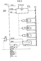
- FIG. 1 An example of a functional unit FUj is shown in FIG. This contains a register set made up of several registers A-REG, B-REG C-REG, which can be loaded or read via a bus system.
- a bus and register control unit BRC is assigned to this register set. It is clocked by an operating clock counter CLK and receives z. B. from a micro program memory, not shown, control signals CTROL for register addressing.
- an input / output register S-REG with parallel inputs and outputs is connected to the bus system BUS. It is designed as a shift register, its serial input is supplied with the data signal DFRSVP via the interface FIF to the interface adapter SIA, while at its serial output the data signal DTOSVP is supplied with the interface adapter to the interface adapter SIA is delivered.
- This input / output register S-REG is effective as a series-parallel converter or as a parallel-series converter during maintenance operations.
- a command broadcast CMD is issued by the maintenance processor SVP via the interface adapter SIA, with the z. B. the operation "read register” is defined, then this command is transmitted to the bus and register control unit BRC via the command signals COMRi which have been declared valid with the first strobe pulse SCOM.
- This maintenance command defined by the command signals COMRi, prevails over the operational register addressing with the control signals CTROL and defines a source register, e.g. B. A-REG.
- the target register is the input / output register S-REG.
- the bus system BUS transfers the content of the source register defined by the maintenance command to the input / output register S-REG, clocked with the second strobe pulse STRANS.
- this strobe pulse is fed in parallel to the third strobe pulse for bit-serial data input or data output SSHIFT via a second OR gate to the input / output register S-REG via the interface FIF from the interface adapter SIA.
- the input / output register S-REG is switched to a functional state "slide right" by the shift pulse SEIFT supplied via the interface FIF.
- the data contained in the input / output register S-REG can thus be transferred bit by bit as data signals DTOSVP, clocked by the third strobe pulse SSHIFT, to the interface adapter SIA and from there to the maintenance processor SVP.
- this data via the second multiplexer MX2 of the interface adapter SIA as data signals DFRSVP from the maintenance processor to the functional unit back into the input / output register S-REG are transferred so that the content of this register is restored.
- the maintenance processor SVP can also transfer certain bit patterns into a selected register of the functional unit FUj.
- the maintenance processor SVP initiates such an operation with a command transmission CMD “load register”.
- the maintenance command including the register address, which is temporarily stored in the command register COMR of the interface adapter SIA, is transferred via the lines for the command signals COMRi to the bus and register control unit BRC with the first strobe pulse SCOMR.
- the input / output register is switched from the SIA interface adapter with the SHIFT shift pulse to the "slide right" function state.
- the data transmitted by the maintenance processor SVP can thus be written bit by bit as data signals DFRSVP into the input / output register S-REG, controlled by the third strobe pulse SSHIFT.
- the target register address is also defined, which prevails over the operational register addressing.
- the source register is the input / output register S-REG.
- the transfer of this register content from the bus system BUS into the selected target register z. B. B-REG is clocked by the fourth strobe SDAT.
- the circuit structure is very flexible.
- the input / output register S-REG can also be used for normal operation, since the maintenance state corresponds to the stop state of the functional unit. Then the input / output register S-REG should also be able to be addressed explicitly from the maintenance processor SVP via the command signals COMRi.
- the interface adapter SIA With this circuit structure, it can also be determined which signals are to be stored as status signals of a functional unit FUj in the interface adapter SIA. These signals can be read by the maintenance processor SVP without the internal resources of the functional unit being required for it, so they can also be determined in the normal case of operation.
- the SIA interface adapter also offers the option, in exceptional cases, of widening the COMR command register or the STAR status register using externally connected shift registers.
- parity-secured registers or memories are to be loaded or read via parity-secured buses, it is usually a good idea to set up the input / output register S-REG in such a way that the associated parity bit runs before 8 data bits in each case during bit-serial reading.
- the maintenance processor SVP can generate the hardware parity bits during loading or check them during reading.
- transparent mode only transmission from and to the maintenance processor in transparent mode is possible, in which all data bits are treated equally. will.
- the transparent mode also enables that parity bits, software-controlled, can be changed in registers as desired, this is very important for diagnostic purposes.
Landscapes
- Engineering & Computer Science (AREA)
- Theoretical Computer Science (AREA)
- General Engineering & Computer Science (AREA)
- Quality & Reliability (AREA)
- Physics & Mathematics (AREA)
- General Physics & Mathematics (AREA)
- Computer Hardware Design (AREA)
- Test And Diagnosis Of Digital Computers (AREA)
- Debugging And Monitoring (AREA)
- Information Transfer Systems (AREA)
- Hardware Redundancy (AREA)
Priority Applications (1)
| Application Number | Priority Date | Filing Date | Title |
|---|---|---|---|
| AT79103076T ATE1437T1 (de) | 1978-09-29 | 1979-08-21 | Verfahren und schnittstellenadapter zum durchfuehren von wartungsoperationen ueber eine schnittstelle zwischen einem wartungsprozessor und einer mehrzahl einzeln zu pruefender funktionseinheiten eines datenverarbeitenden systems. |
Applications Claiming Priority (2)
| Application Number | Priority Date | Filing Date | Title |
|---|---|---|---|
| DE2842603A DE2842603C3 (de) | 1978-09-29 | 1978-09-29 | Schnittstelle zwischen einem Wartungsprozessor und einer Mehrzahl einzeln zu prüfender Funktionseinheiten eines datenverarbeitenden Systems |
| DE2842603 | 1978-09-29 |
Publications (3)
| Publication Number | Publication Date |
|---|---|
| EP0009600A2 true EP0009600A2 (fr) | 1980-04-16 |
| EP0009600A3 EP0009600A3 (en) | 1980-04-30 |
| EP0009600B1 EP0009600B1 (fr) | 1982-08-04 |
Family
ID=6050945
Family Applications (1)
| Application Number | Title | Priority Date | Filing Date |
|---|---|---|---|
| EP79103076A Expired EP0009600B1 (fr) | 1978-09-29 | 1979-08-21 | Procédé et dispositif d'interface pour exécuter des operations de maintenance sur une interface entre un processeur de maintenance et une pluralité d'unités fonctionnelles à vérifier d'un système de traitement de données |
Country Status (3)
| Country | Link |
|---|---|
| EP (1) | EP0009600B1 (fr) |
| AT (1) | ATE1437T1 (fr) |
| DE (1) | DE2842603C3 (fr) |
Cited By (6)
| Publication number | Priority date | Publication date | Assignee | Title |
|---|---|---|---|---|
| EP0105121A1 (fr) * | 1982-10-06 | 1984-04-11 | International Business Machines Corporation | Procédé pour détecter un défaut dans un canal de lecture pour système d'enregistrement de données |
| EP0301248A1 (fr) * | 1987-06-30 | 1989-02-01 | Siemens Nixdorf Informationssysteme Aktiengesellschaft | Installation de traitement de données avec processeur de maintenance et procédé pour exécuter telles opérations de maintenance |
| EP0247605A3 (en) * | 1986-05-30 | 1989-08-16 | Honeywell Bull Inc. | System management apparatus for a multiprocessor system |
| EP0276445A3 (en) * | 1987-01-30 | 1990-03-21 | International Business Machines Corporation | Method and apparatus for detecting transient errors |
| EP0389660A1 (fr) * | 1989-03-30 | 1990-10-03 | Siemens Nixdorf Informationssysteme Aktiengesellschaft | Agencement de circuit pour installations de traitement de données ayant des unités fonctionnelles commandées par exécution de micro instructions |
| FR2657182A1 (fr) * | 1990-01-15 | 1991-07-19 | Cit Alcatel | Dispositif d'aide au diagnostic. |
Families Citing this family (2)
| Publication number | Priority date | Publication date | Assignee | Title |
|---|---|---|---|---|
| DE3441227A1 (de) * | 1984-11-10 | 1986-05-15 | Philips Patentverwaltung Gmbh, 2000 Hamburg | Schaltungsanordnung zur ueberwachung mehrerer sammelleitungen |
| US7093764B1 (en) | 2001-04-20 | 2006-08-22 | Palm, Inc. | Integrated SIM holder with backcase and rotating door |
Family Cites Families (3)
| Publication number | Priority date | Publication date | Assignee | Title |
|---|---|---|---|---|
| DE2350371C3 (de) * | 1973-10-08 | 1981-03-26 | IBM Deutschland GmbH, 70569 Stuttgart | Verfahren und Einrichtung zur Prüfung und Wartung von Datenverarbeitungsanlagen mittels räumlich entfernter Wartungsstationen |
| US3921139A (en) * | 1974-03-08 | 1975-11-18 | Westinghouse Electric Corp | Test system having memory means at test module |
| US3997879A (en) * | 1975-12-24 | 1976-12-14 | Allen-Bradley Company | Fault processor for programmable controller with remote I/O interface racks |
-
1978
- 1978-09-29 DE DE2842603A patent/DE2842603C3/de not_active Expired
-
1979
- 1979-08-21 EP EP79103076A patent/EP0009600B1/fr not_active Expired
- 1979-08-21 AT AT79103076T patent/ATE1437T1/de not_active IP Right Cessation
Cited By (6)
| Publication number | Priority date | Publication date | Assignee | Title |
|---|---|---|---|---|
| EP0105121A1 (fr) * | 1982-10-06 | 1984-04-11 | International Business Machines Corporation | Procédé pour détecter un défaut dans un canal de lecture pour système d'enregistrement de données |
| EP0247605A3 (en) * | 1986-05-30 | 1989-08-16 | Honeywell Bull Inc. | System management apparatus for a multiprocessor system |
| EP0276445A3 (en) * | 1987-01-30 | 1990-03-21 | International Business Machines Corporation | Method and apparatus for detecting transient errors |
| EP0301248A1 (fr) * | 1987-06-30 | 1989-02-01 | Siemens Nixdorf Informationssysteme Aktiengesellschaft | Installation de traitement de données avec processeur de maintenance et procédé pour exécuter telles opérations de maintenance |
| EP0389660A1 (fr) * | 1989-03-30 | 1990-10-03 | Siemens Nixdorf Informationssysteme Aktiengesellschaft | Agencement de circuit pour installations de traitement de données ayant des unités fonctionnelles commandées par exécution de micro instructions |
| FR2657182A1 (fr) * | 1990-01-15 | 1991-07-19 | Cit Alcatel | Dispositif d'aide au diagnostic. |
Also Published As
| Publication number | Publication date |
|---|---|
| EP0009600B1 (fr) | 1982-08-04 |
| ATE1437T1 (de) | 1982-08-15 |
| DE2842603B2 (de) | 1980-07-17 |
| DE2842603C3 (de) | 1981-06-11 |
| EP0009600A3 (en) | 1980-04-30 |
| DE2842603A1 (de) | 1980-04-03 |
Similar Documents
| Publication | Publication Date | Title |
|---|---|---|
| DE2614000C2 (de) | Diagnoseeinrichtung zur Prüfung von Funktionseinheiten | |
| DE2921387C2 (de) | Verfahren zum Austauschen von Informationen zwischen einer Datenverarbeitungsanlage und einem Magnetplattenspeicher | |
| DE2856483C2 (fr) | ||
| DE3121540C3 (de) | Signalübertragungsvorrichtung für den Datenaustausch zwischen zwei Mikroprozessor-Informationsverarbeitungsstationen | |
| DE3300260C2 (fr) | ||
| DE69332051T2 (de) | System zum Steuern von Testlogik mit Boundary-Scan in einem Kommunikationsnetz | |
| DE2741886A1 (de) | Datenuebertragungseinrichtung | |
| DE112020004065T5 (de) | Komplexe Daisy-Chain-Befehle | |
| DE69029643T2 (de) | Kanal für Datenverarbeitungssystem | |
| DE2536625C2 (de) | Paritätsprüfschaltung für ein binär zählendes Register | |
| DE3780307T2 (de) | Protokoll und anordnung zur verbindung zwischen einer steuereinheit und mehreren peripheren elementen. | |
| EP0009600A2 (fr) | Procédé et dispositif d'interface pour exécuter des operations de maintenance sur une interface entre un processeur de maintenance et une pluralité d'unités fonctionnelles à vérifier d'un système de traitement de données | |
| DE2517170C2 (de) | Schaltungsanordnung zum Unterbrechen des Programmablaufs in Datenverarbeitungsanlagen mit mehreren Ansteuereinrichtungen von Sekundärspeichern und dergleichen Speichereinheiten mit sequentiellem Zugriff | |
| DE69112516T2 (de) | Schnittstellenmodul für Datenübertragung. | |
| DE3137904C2 (de) | Schaltungsanordnung für Fernmeldevermittlungsanlagen, insbesondere Fernsprechvermittlungsanlagen, mit Einrichtungen zur Sicherung der Übertragung codierter Signale | |
| DE60202697T2 (de) | Asynchrone datenübertragungsanordnung mit steuerungsmittel für taktabweichungen | |
| DE69126249T2 (de) | Verarbeitungsvorrichtung und Verfahren zur Programmierung einer solchen Vorrichtung | |
| EP0029216B1 (fr) | Dispositif pour la transmission de données avec une mémoire-tampon et dispositifs pour la protection des données | |
| DE1164714B (de) | Verfahren zur Pruefung der Datenuebertragung in elektronischen Datenverarbeitungssystemen | |
| DE69315785T2 (de) | Modulare Vorrichtung zum Koppeln und zum Multiplexen von unterschiedlichen Bussen | |
| EP0012794B1 (fr) | Procédé et dispositif pour vérifier les signaux de commande déduits de l'instruction d'une unité électronique de traitement de données | |
| DE102009000698A1 (de) | Prüfschaltung zur Prüfung einer Durchführung eines Handshake-Protokolls und Verfahren zur Prüfung einer Durchführung eines Handshake-Protokolls | |
| EP0214475B1 (fr) | Circuit pour transmettre des signaux de données entre des dispositifs de commande reliées entre eux par un système en anneaux | |
| DE2846487A1 (de) | Datenverarbeitungssystem | |
| DE4244275C1 (de) | Nachprüfung der Datenintegrität bei gepufferter Datenübertragung |
Legal Events
| Date | Code | Title | Description |
|---|---|---|---|
| PUAI | Public reference made under article 153(3) epc to a published international application that has entered the european phase |
Free format text: ORIGINAL CODE: 0009012 |
|
| PUAL | Search report despatched |
Free format text: ORIGINAL CODE: 0009013 |
|
| AK | Designated contracting states |
Designated state(s): AT BE CH FR GB IT NL |
|
| AK | Designated contracting states |
Designated state(s): AT BE CH FR GB IT NL |
|
| 17P | Request for examination filed | ||
| ITF | It: translation for a ep patent filed | ||
| GRAA | (expected) grant |
Free format text: ORIGINAL CODE: 0009210 |
|
| AK | Designated contracting states |
Designated state(s): AT BE CH FR GB IT NL |
|
| REF | Corresponds to: |
Ref document number: 1437 Country of ref document: AT Date of ref document: 19820815 Kind code of ref document: T |
|
| PGFP | Annual fee paid to national office [announced via postgrant information from national office to epo] |
Ref country code: GB Payment date: 19910718 Year of fee payment: 13 |
|
| PGFP | Annual fee paid to national office [announced via postgrant information from national office to epo] |
Ref country code: AT Payment date: 19910726 Year of fee payment: 13 |
|
| PGFP | Annual fee paid to national office [announced via postgrant information from national office to epo] |
Ref country code: FR Payment date: 19910823 Year of fee payment: 13 |
|
| PGFP | Annual fee paid to national office [announced via postgrant information from national office to epo] |
Ref country code: BE Payment date: 19910828 Year of fee payment: 13 |
|
| ITTA | It: last paid annual fee | ||
| PGFP | Annual fee paid to national office [announced via postgrant information from national office to epo] |
Ref country code: NL Payment date: 19910831 Year of fee payment: 13 |
|
| PGFP | Annual fee paid to national office [announced via postgrant information from national office to epo] |
Ref country code: CH Payment date: 19911122 Year of fee payment: 13 |
|
| PG25 | Lapsed in a contracting state [announced via postgrant information from national office to epo] |
Ref country code: GB Effective date: 19920821 Ref country code: AT Effective date: 19920821 |
|
| PG25 | Lapsed in a contracting state [announced via postgrant information from national office to epo] |
Ref country code: CH Effective date: 19920831 Ref country code: BE Effective date: 19920831 |
|
| BERE | Be: lapsed |
Owner name: SIEMENS A.G. BERLIN UND MUNCHEN Effective date: 19920831 |
|
| PG25 | Lapsed in a contracting state [announced via postgrant information from national office to epo] |
Ref country code: NL Effective date: 19930301 |
|
| NLV4 | Nl: lapsed or anulled due to non-payment of the annual fee | ||
| GBPC | Gb: european patent ceased through non-payment of renewal fee |
Effective date: 19920821 |
|
| PG25 | Lapsed in a contracting state [announced via postgrant information from national office to epo] |
Ref country code: FR Effective date: 19930430 |
|
| REG | Reference to a national code |
Ref country code: CH Ref legal event code: PL |
|
| REG | Reference to a national code |
Ref country code: FR Ref legal event code: ST |
|
| PLBE | No opposition filed within time limit |
Free format text: ORIGINAL CODE: 0009261 |
|
| STAA | Information on the status of an ep patent application or granted ep patent |
Free format text: STATUS: NO OPPOSITION FILED WITHIN TIME LIMIT |