EP0009910B1 - Dispositif de mémoire à semiconducteurs et procédé de fabrication de ce dispositif - Google Patents
Dispositif de mémoire à semiconducteurs et procédé de fabrication de ce dispositif Download PDFInfo
- Publication number
- EP0009910B1 EP0009910B1 EP79301928A EP79301928A EP0009910B1 EP 0009910 B1 EP0009910 B1 EP 0009910B1 EP 79301928 A EP79301928 A EP 79301928A EP 79301928 A EP79301928 A EP 79301928A EP 0009910 B1 EP0009910 B1 EP 0009910B1
- Authority
- EP
- European Patent Office
- Prior art keywords
- region
- semiconductor
- single crystalline
- layer
- polycrystalline
- Prior art date
- Legal status (The legal status is an assumption and is not a legal conclusion. Google has not performed a legal analysis and makes no representation as to the accuracy of the status listed.)
- Expired
Links
Images


Classifications
-
- G—PHYSICS
- G11—INFORMATION STORAGE
- G11C—STATIC STORES
- G11C11/00—Digital stores characterised by the use of particular electric or magnetic storage elements; Storage elements therefor
- G11C11/21—Digital stores characterised by the use of particular electric or magnetic storage elements; Storage elements therefor using electric elements
- G11C11/34—Digital stores characterised by the use of particular electric or magnetic storage elements; Storage elements therefor using electric elements using semiconductor devices
- G11C11/40—Digital stores characterised by the use of particular electric or magnetic storage elements; Storage elements therefor using electric elements using semiconductor devices using transistors
- G11C11/401—Digital stores characterised by the use of particular electric or magnetic storage elements; Storage elements therefor using electric elements using semiconductor devices using transistors forming cells needing refreshing or charge regeneration, i.e. dynamic cells
- G11C11/403—Digital stores characterised by the use of particular electric or magnetic storage elements; Storage elements therefor using electric elements using semiconductor devices using transistors forming cells needing refreshing or charge regeneration, i.e. dynamic cells with charge regeneration common to a multiplicity of memory cells, i.e. external refresh
- G11C11/404—Digital stores characterised by the use of particular electric or magnetic storage elements; Storage elements therefor using electric elements using semiconductor devices using transistors forming cells needing refreshing or charge regeneration, i.e. dynamic cells with charge regeneration common to a multiplicity of memory cells, i.e. external refresh with one charge-transfer gate, e.g. MOS transistor, per cell
-
- H—ELECTRICITY
- H10—SEMICONDUCTOR DEVICES; ELECTRIC SOLID-STATE DEVICES NOT OTHERWISE PROVIDED FOR
- H10B—ELECTRONIC MEMORY DEVICES
- H10B12/00—Dynamic random access memory [DRAM] devices
- H10B12/30—DRAM devices comprising one-transistor - one-capacitor [1T-1C] memory cells
- H10B12/33—DRAM devices comprising one-transistor - one-capacitor [1T-1C] memory cells the capacitor extending under the transistor
-
- H—ELECTRICITY
- H10—SEMICONDUCTOR DEVICES; ELECTRIC SOLID-STATE DEVICES NOT OTHERWISE PROVIDED FOR
- H10P—GENERIC PROCESSES OR APPARATUS FOR THE MANUFACTURE OR TREATMENT OF DEVICES COVERED BY CLASS H10
- H10P32/00—Diffusion of dopants within, into or out of wafers, substrates or parts of devices
- H10P32/10—Diffusion of dopants within, into or out of semiconductor bodies or layers
- H10P32/14—Diffusion of dopants within, into or out of semiconductor bodies or layers within a single semiconductor body or layer in a solid phase; between different semiconductor bodies or layers, both in a solid phase
- H10P32/1408—Diffusion of dopants within, into or out of semiconductor bodies or layers within a single semiconductor body or layer in a solid phase; between different semiconductor bodies or layers, both in a solid phase from or through or into an external applied layer, e.g. photoresist or nitride layers
- H10P32/1414—Diffusion of dopants within, into or out of semiconductor bodies or layers within a single semiconductor body or layer in a solid phase; between different semiconductor bodies or layers, both in a solid phase from or through or into an external applied layer, e.g. photoresist or nitride layers the applied layer being silicon, silicide or SIPOS, e.g. polysilicon or porous silicon
-
- H—ELECTRICITY
- H10—SEMICONDUCTOR DEVICES; ELECTRIC SOLID-STATE DEVICES NOT OTHERWISE PROVIDED FOR
- H10P—GENERIC PROCESSES OR APPARATUS FOR THE MANUFACTURE OR TREATMENT OF DEVICES COVERED BY CLASS H10
- H10P32/00—Diffusion of dopants within, into or out of wafers, substrates or parts of devices
- H10P32/10—Diffusion of dopants within, into or out of semiconductor bodies or layers
- H10P32/17—Diffusion of dopants within, into or out of semiconductor bodies or layers characterised by the semiconductor material
- H10P32/171—Diffusion of dopants within, into or out of semiconductor bodies or layers characterised by the semiconductor material being group IV material
-
- H—ELECTRICITY
- H10—SEMICONDUCTOR DEVICES; ELECTRIC SOLID-STATE DEVICES NOT OTHERWISE PROVIDED FOR
- H10W—GENERIC PACKAGES, INTERCONNECTIONS, CONNECTORS OR OTHER CONSTRUCTIONAL DETAILS OF DEVICES COVERED BY CLASS H10
- H10W10/00—Isolation regions in semiconductor bodies between components of integrated devices
- H10W10/01—Manufacture or treatment
- H10W10/041—Manufacture or treatment of isolation regions comprising polycrystalline semiconductor materials
-
- H—ELECTRICITY
- H10—SEMICONDUCTOR DEVICES; ELECTRIC SOLID-STATE DEVICES NOT OTHERWISE PROVIDED FOR
- H10W—GENERIC PACKAGES, INTERCONNECTIONS, CONNECTORS OR OTHER CONSTRUCTIONAL DETAILS OF DEVICES COVERED BY CLASS H10
- H10W10/00—Isolation regions in semiconductor bodies between components of integrated devices
- H10W10/40—Isolation regions comprising polycrystalline semiconductor materials
-
- H—ELECTRICITY
- H10—SEMICONDUCTOR DEVICES; ELECTRIC SOLID-STATE DEVICES NOT OTHERWISE PROVIDED FOR
- H10W—GENERIC PACKAGES, INTERCONNECTIONS, CONNECTORS OR OTHER CONSTRUCTIONAL DETAILS OF DEVICES COVERED BY CLASS H10
- H10W20/00—Interconnections in chips, wafers or substrates
- H10W20/01—Manufacture or treatment
- H10W20/021—Manufacture or treatment of interconnections within wafers or substrates
Definitions
- This invention relates to a semiconductor memory device comprising a plurality of memory cells each comprising an MOS transistor and an electric-charge storage region, the device being of the dynamic MOS (metal oxide semiconductor) - RAM (random access memory) type, and to a process for producing the device.
- a semiconductor memory device comprising a plurality of memory cells each comprising an MOS transistor and an electric-charge storage region, the device being of the dynamic MOS (metal oxide semiconductor) - RAM (random access memory) type, and to a process for producing the device.
- MOS - RAM cells are those in which one MOS transfer gate is combined with one memory capacitor utilising a so-called MOS capacitor.
- MOS - RAM cell the memory capacitor is situated on the same surface of a semiconductor substrate as the transfer gate and occupies a considerable area of 30% or more of the memory cell. Since a constant electrical potential must be supplied to the MOS capacitor from outside the memory cell, the layout of the elements of the memory device is limited due to the existence of a metal line for supplying the potential to the MOS capacitor.
- a dual polycrystalline silicon process which is employed for the production of the MOS capacitor and the transfer gate, makes the production process of the memory cell complicated, because insulation' between the two layers of polycrystalline silicon and a very accurate photolithography process are required.
- the production yield of the memory cell is decreased, due to the dual polycrystalline silicon structure, from that of the yield of the conventional MOS - RAMs.
- the low yield of the MOS - RAMs is attributed mainly to a thin oxide film of the capacitor, which oxide film covers a large surface area of the semiconductor substrate, because such an oxide film is liable to be defective, and further, a gate-oxide short circuit is liable to be caused by fine particles on the silicon of the semiconductor substrate.
- stored charges are liable to leak through a path on the substrate surface, which path is formed due to an accidentally contaminated surface portion of the substrate.
- a semiconductor memory device besides that utilising the MOS capacitor mentioned above, is known from United States Patent No. 4,003,036, in which device a junction capacitance created by a buried diffusion layer in the semiconductor substrate is utilised for a memory capacitor.
- the memory device disclosed in the U.S. Patent mentioned above is a so-called VMOS transistor and eliminates all the drawbacks of the memory device utilising the MOS capacitor.
- VMOS transistor a special etching process required for the formation of the V grooves causes a low production yield of the VMOS transistor, which is a problem.
- special caution must be taken to prevent the disconnection of the metal lines due to the steep V grooves. It is therefore, difficult to use conventional aluminium wiring and the like, due to the steep V grooves.
- the production process of the VMOS transistor and layout of the elements of such transistor cannot be modified freely, which is another disadvantage.
- One-transistor memory cells in which the capacitance charge storage region is located beneath the transfer gate are known from an article "Single FET Memory Cell with Buried Extended Source” by N. G. Anantha et al in IBM Technical Disclosure Bulletin, Volume 16, No. 8, January 1974, pages 2708-2709, and article "MOSFET Memory Cell using Junction Capacitance” by S. A. Abbas in IBM Technical Disclosure Bulletin, Volume 18, No. 10, March 1976, page 3300.
- memory cells each formed by an MOS transistor and an electric-charge storage region comprise a substrate of a semiconductor material, a semiconductor growth layer having a single crystalline region, and a semiconductor layer individual to each cell, of different conductivity type from the substrate, buried between the substrate and the semiconductor growth layer.
- the buried semiconductor layers are used as the electric-charge storage regions of respective cells.
- United States Patent No. 3,947,299 discloses an integrated circuit having buried insulating layers on which polycrystalline zones are formed.
- Fig. 19 after oxidation of a section of one of the polycrystalline zones down to the layer to provide inset insulation, dopant is diffused into the remainder of the zone and hence into the adjoining monocrystalline material to provide a connection to the surface from a buried base region.
- a semiconductor memory device including a plurality of memory cells, each formed by an MOS transistor and an electric-charge storage region, and comprising a common substrate of a semiconductor material having one type of conductivity, a semiconductor growth layer on the substrate, comprising a single crystalline region, and for each cell a semiconductor layer, having the opposite type of conductivity, buried between the substrate and the semiconductor growth layer which buried layer is used as the electric-charge storage region of the cell, characterised in that for each memory cell a source or drain region is constituted by a first single crystalline impurity-doped region of the same conductivity type as the buried semiconductor layer formed on a selected portion of the single crystalline region; in that a buried insulating layer is disposed adjacent each buried semiconductor layer; in that for each cell a polycrystalline region having the same type of conductivity as the buried semiconductor layers is located on the buried insulating layer; in that a second single crystalline impurity-doped portion, having the same type of
- a process for fabricating a semiconductor memory device comprising a plurality of memory cells each formed by an MOS transistor and an electric-charge storage region, the process comprising selectively forming, at a surface of a semiconductor substrate of one conductivity type, semiconductor layers of the opposite conductivity type to act as storage regions, growing a semiconductor layer of said one conductivity type comprising a single crystalline region on the semiconductor substrate to bury said layers, and introducing impurities of the same conductivity type as the buried semiconductor layers into selected areas of the single crystalline region so as to form first impurity-doped regions of transistors of the memory cells, characterised in that an insulating layer is selectively formed on a surface of the semiconductor substrate adjacent each said semiconductor storage region layer, that the semiconductor layer is then grown to form a polycrystalline portion over the insulating layer and single crystalline portions bounded by the polycrystalline portion and each overlying at least one storage region layer, that said impurities are introduced into a selected surface area of each single crystalline portion to
- a transfer region is defined between the first single crystalline impurity-doped region and the shallow drain or source region, and a planar transfer electrode is formed on the transfer region.
- a planar transfer electrode is formed on the transfer region.
- the polycrystalline region which is a portion of the semiconductor growth layer, preferably extends in the form of a column and such columnar polycrystalline region plays an important role in electrically connecting the transfer region with the buried semiconductor layer. It is to be noted regarding the electrical connection, that the diffusion rate of impurities in the polycrystalline region is three times or more higher than that in the single crystalline region. As a result, until the formation of the first single crystalline impurity-doped portion, the second single crystalline impurity-doped portion extends in a vertical direction as far as the buried semiconductor layer. The formation of such single crystalline impurity-doped portion is due to permeation of the diffused impurities in the polycrystalline columnar region into the single crystalline region via the interface between the polycrystalline and single crystalline regions.
- the single crystalline impurity-doped portion extends vertically downwards to the buried semiconductor layer, as explained above. It is possible to produce by a single thermal diffusion the shallow source and drain as well as the deep vertical connecting portion.
- the semiconductor growth layer is fabricated in such a manner that a firstly grown P + (N + ) type layer, which has single crystalline and polycrystalline regions, has a high impurity concentration in the range of from 5 x 1 016 to 5 ⁇ 10 18 /cm 3 , and further, a secondly grown P-(N-) type layer, which has single crystalline and polycrystalline portions, has a low impurity concentration in the range of from 5 X J0 13 to 5x 10'S/cm3.
- the reason for forming the P + (N + ) type layer is to prevent an up-diffusion of the N(P) type impurities from the N + (P + ) type buried semiconductor layer into the epitaxially grown single crystalline region of the semiconductor growth layer, and thus, converting the conductivity type of this region to N(P) type, and; also to enhance a punch-through voltage between the N + (P + ) type buried semiconductor layer and the N + (P + ) type first impurity doped region.
- the source electrode or the drain electrode of the MOS transistor comprises impurity-doped polycrystalline silicon and is formed on the single crystalline and polycrystalline regions of the semiconductor growth layer, in such a manner that that electrode extends across the boundary between these regions.
- the other of the source and drain electrodes comprises the impurity-doped polycrystalline silicon and is formed on a portion of the single crystalline region of the semiconductor growth layer.
- a gate oxide film of the MOS transistor is formed between the source and drain electrodes.
- the impurities such as arsenic
- the impurities may be diffused by heat treatment, under a non-oxidizing atmosphere, from the source and drain electrodes, thereby diffusing the impurities quickly through the polycrystalline region and, then, permeating the so- diffused impurities into the single crystalline region.
- the second single crystalline impurity-doped region formed by permeation, extends to the buried semiconductor layer.
- the impurities are slowly diffused into the single crystalline region, thereby forming the shallow first single crystalline impurity-doped region.
- the impurity-doped regions are formed below the source and drain electrodes and essentially no lateral diffusion of the impurities occurs.
- the overlapping capacitance between the gate and either of the source or drain is therefore low, and further, a virtual self-alignment is achieved.
- the source and drain electrodes are doped to a high concentration of from 1 x 10 2 ° to 1 x 10 21 / CM 3 , the resistance of the source and drain becomes low.
- the source and drain can be constructed as thin diffused regions, as stated above, and the diffusion depth is usually from 500 to 3000A. Generally, both of the requirements that the source and drain regions of the MOS transistor are shallow and that they have a low resistance should be satisfied in order to provide the MOS transistor with a high speed and a high mutual conductance (Gm).
- This embodiment of the present invention in which these requirements are satisfied, is suitable for an MIS semiconductor device having a short channel length and is suitable for a highly integrated RAM.
- the impurity diffusion from the source and drain electrodes is carried out before the formation of the gate electrodes. Accordingly, it is possible to use for the electrodes an aluminum gate, which is suitable for a high speed memory. In the case of using the aluminum gate, the formation of all the oxides in the succeeding stages must rely on a chemical vapor deposition (CVD).
- the memory device of this embodiment is different from the conventional memory device in the fact that no contact windows for the electrodes are necessary in the memory cells. Therefore, no such problems as deviation of mask alignment in the production of the contact windows, and poor contact between the electrodes and the substrate occurs in this embodiment. In addition, the production yield of the memory device is high, because no photolithographic process is employed for the formation of the contact windows.
- a thick oxide film on the source and drain electrodes, of heavily doped silicon is formed by a preferential oxidation process at a low temperature of 900°C or lower, under a moist or wet atmosphere, such as a water-vapor atmosphere.
- the oxide film is also formed on the intermediate surface portion of the lightly doped single crystalline silicon of the semiconductor growth layer between the source and drain electrodes.
- the oxide film is thicker on the heavily doped silicon than the lightly doped silicon, and thus, it is possible to etch the oxide film so as to leave only the thick oxide.
- a high temperature oxidation at a temperature of 1000°C or higher, is carried out. Accordingly, it is possible to remove any danger of expansion of the impurity-diffusion layers or regions, such as the buried semiconductor layer which is a carrier- storage region of the MOS - RAM, during the heat treatment for the high temperature oxidation.
- a pair of memory cells is provided with a common gate oxide film.
- this embodiment may be modified so that each of the memory cells is provided with its own gate oxide film.
- N + type impurities of arsenic are diffused by a conventional gas-phase diffusion process into a P + type silicon semiconductor substrate 1 of a resistivity ranging from 0.5 to 1.1 ⁇ cm, with the result that N + type silicon layers 2 of a thickness of from 5000 to 20000A are formed. These layers become buried layers in the succeeding step and are referred to herein as N + type buried silicon layers 2.
- a silicon dioxide film 3 is selectively formed by thermal oxidation, so as to surround a pair of the N + type buried silicon layers 2.
- a thin P + type silicon semiconductor growth layer 4S and 4P is firstly formed on the P + type silicon semiconductor substrate 1 and a thick P- type or nondoped silicon semiconductor growth layer 5S, 5P is then formed on the thin P + type silicon semiconductor layer 4P and 4S, by a conventional epitaxial growth process.
- a single crystalline region and polycrystalline region grow on the exposed surface of the P + type silicon semiconductor substrate 1 and the silicon dioxide film 3.
- the firstly grown P + type single crystalline region and polycrystalline region are denoted as 4S and 4P, respectively.
- regions 4S and 4P have an impurity concentration of from 5 ⁇ 10 16 to 5 ⁇ 10 18 /cm 3 , preferably from 5 ⁇ 10 17 to 1 x 10 18 /cm 3 , and a thickness of from 2000 to 3000A.
- the secondly grown P-type, single crystalline region and polycrystalline region are denoted as 5S and 5P, respectively.
- These regions have an impurity concentration of from 5 ⁇ 10 13 to 5 ⁇ 10 15 /cm 3 , preferably from 1 x 10' 4 to 1 x 1 015/cm3, and a thickness of from 5000 to 10000A.
- an oxide film 6 for isolation is formed by a selective oxidation process on the middle portion of the polycrystalline regions 4P and 5P, so as to isolate the portions of the semiconductor growth layers 4S, 4P, 5S and 5P, which become memory cells, from each other.
- a thin silicon dioxide film 7 of a thickness ranging from 200 to 1000A is formed by thermal oxidation.
- a boron ion implantation is performed at a concentration of from 1 ⁇ 10 11 to 2 ⁇ 10 12 ions/cm 2 and an ion energy of, for example, 50 KeV, so as to implant the boron ions on the entire surface of the silicon dioxide film 7, as shown by the arrows in Fig. 4.
- a threshold voltage Vth of the MOS transistor is adjusted.
- a polycrystalline silicon film 8 heavily doped with N type impurities, namely phosphorus or arsenic, is then grown.
- the polycrystalline silicon film 8 may have a thickness ranging from 3000 to 5000A and an impurity concentration ranging from 5x 10 20 to 2x 10 21 /cm 3 .
- the silicon dioxide film 7 and the polycrystalline silicon film 8 are then delineated by a conventional photolithography technique, so that the silicon dioxide film 7 and the polycrystalline silicon film 8 are provided with a pattern of gate insulating film and a pattern of gate electrodes, respectively.
- the gate insulating film and the gate electrodes are also indicated by reference numerals 7 and 8, respectively.
- an oxide film covering the polycrystalline silicon gate electrodes 8 is formed by thermal oxidation at a low temperature of, for example, from 800 to 900°C, under a moist atmosphere.
- This oxide film is also indicated by 7.
- the P" type single crystalline and polycrystalline regions 5S and 5P, which are not covered by polycrystalline silicon gate electrodes (word lines) 8, are oxidized during the thermal oxidation, the oxide on these regions 5S and 5P has a thickness considerably less than that on the polycrystalline silicon gate electrodes 8, which are heavily doped with the N type impurities.
- the oxide on the regions 5S and 5P is, therefore, removed by etching after the thermal oxidation.
- the oxide film 7 is, therefore, left as shown in Fig. 5.
- a phosphosilicate glass film 9 is grown and a heat treatment at a temperature of from 900 to 1100°C is carried out, so as to diffuse the phosphorus contained in the glass film 9 into the silicon growth layers 4S, 4P, 5P and 5S.
- the first N+ type impurity portion, denoted as 10 is formed on the surface of the single crystalline region 5S.
- the second N + type impurity portions denoted as 11, are formed in the single crystalline regions 5S and 4S.
- One of these portions 10 and 11 defines the source region and the other defines the drain region.
- N + type impurity-doped portions 11 a of the second single crystalline impurities portions which constitute a vertical connection between the N + type buried layers 2 and the drain or source 11, are simultaneously formed with the formation of the source or drain 10.
- the technique used for forming the impurity-doped portions 10 and 11 is not limited to the diffusion between the solid phases, and may be any other process, such as ion implantation of arsenic ions.
- the phosphosilicate glass layer 9 is delineated by a conventional photolithography technique into a pattern of an electrode. Subsequently an aluminum film 12 is formed by an evaporation process and is also delineated by a conventional photolithography technique into an electrode pattern and wiring, which are also denoted by 12.
- the bit lines of the memory device are defined by the electrodes and wiring 12.
- the structural features of the memory device according to the present invention will be understood from Fig. 7.
- the memory capacitor of the memory device the junction capacitance between the N + type buried semiconductor layers 2 and the P + type silicon semiconductor substrate 1 is used. Accordingly, the memory device according to the present invention exhibits a higher integration degree than a memory device using MOS capacitance, while the drawbacks of memory devices using MOS capacitance are completely eliminated in the present invention.
- Fig. 8 The electrical equivalent circuit of two pairs of memory cells produced as described above is illustrated in Fig. 8.
- the lines WL 1 and WL 2 represent the word lines formed by the silicon gate electrodes 8 illustrated in Fig. 7, while the lines BL, and BL 2 represent the bit lines formed by the aluminum electrode and wiring 12 illustrated in Fig. 7.
- Fig. 9 is a plan view of a representative portion of the semiconductor memory device produced as described above.
- C H indicates a contact window of the bit lines BL 1 and BL 2 with one of the source and drain regions.
- the area surrounded by the chain line denoted by Mc indicates a single memory cell Ps represents the polycrystalline silicon regions 5P and 5S represents the single crystalline region 5S.
- the rectangular silicon areas Ps and Ss are surrounded by the silicon dioxide isolating film 6 (Fig. 7).
- Figs. 1 through 7 are cross-sectional views taken along the line A-A', in Fig. 9, in the direction of the arrows.
- An important feature of the memory cell of the present invention is a significant reduction of the cell size compared to the conventional one transistor RAM cell. As illustrated in Fig. 9, each of these cells has an area of only 6F 2 (3Fx2F), where F is the lithographic minimum feature size.
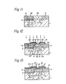
- FIGs. 10 through 13 illustrating another preferred embodiment of the present invention, similar portions to those in Figs. 1 through 7 are identically numbered as in Figs. 1 through 7.
- the N + type layer which becomes the buried layer 2 is formed on the P + type silicon semiconductor substrate 1 (Fig. 10) by introducing N type impurities into the substrate 1 by a conventional vapour-phase diffusion method.
- the N + type layer is referred to herein as the N + type buried semiconductor layer 2.
- the silicon dioxide film 3 is formed by a selective thermal oxidation using, for example, silicon nitride as a mask. The silicon dioxide film 3 partially overlaps the N + buried semiconductor layer 2.
- a thin P + type silicon semiconductor growth layer 4P and 4S (Fig. 11) and, then, a thick P- type or nondoped silicon semiconductor growth layer 5P and 5S are formed by, for example, a conventional vapor-phase growth process.
- the polycrystalline portions 4P and 5P and single crystalline regions 4S and 5S are selectively grown.
- the P type impurities may be boron.
- a selective oxidation process is then employed for the formation of an isolation oxide film 6, which isolates future memory cells from each other.
- a chemical vapor-phase growth may be applied for the formation of the isolation oxide film 6.
- a polycrystalline silicon film (27, 28) containing a heavy doping of arsenic in an amount of from 5x10 2 ° to 2x 10 21 /cm 3 is grown to a thickness of from 3000 to 6000A, for example, approximately 5000 A, and is then delineated by a conventional photolithography technique to the pattern of the source electrode 27 and the drain electrode 28.
- a heat treatment in the non-oxidizing atmosphere is then carried out, thereby diffusing the arsenic from the source electrode 27 and the drain electrode 28.
- the first N+ type impurity portion 10 is formed in the single crystalline region 5S and the second N + type impurity portion 11, vertically extending to the buried semiconductor layer 2, is simultaneously formed. Due to the arsenic diffusion, the polycrystalline regions 4P and 5P (Fig. 11) are changed to a single N + type polycrystalline region, which is denoted as 4P' in Fig. 12.
- an oxide film 29 is formed by a preferential oxidation in a water-vapor atmosphere at a temperature of from 800 to 900°C, thereby forming the oxide film 29 over the surface of the source electrode 27, the drain electrode 28 and the surface of the P- type single crystalline semiconductor regions 5S between the electrodes 27 and 28. It is easy to form an oxide film having a thickness of from 2000 to 3000A over the surface of the source electrode 27 and the drain electrode 28, and to simultaneously form an oxide film (not shown) having a thickness of from 250 to 375A over the surface of the P - type single crystalline substrate.
- the oxide film on the P- type single crystalline semiconductor regions 5S is then removed by an etching, using a solution of hydrofluoric acid (HF), because the oxide film formed by low temperature oxidation is suitable for isolation but does not exhibit a very excellent quality for the gate oxide film.
- the oxide film 6 on the source electrode 27 and the drain electrode 28 is also etched during the removal of the oxide film mentioned, above. However, such etching presents no problem, because the isolation oxide film 6 is thickly formed, as will be understood from the above explanation.
- the gate oxide film 30 of, for example, 500A thickness is then formed by oxidation at a temperature of, for example, 1100°C.
- boron ions are implanted as indicated by the arrows in Fig. 12 at a concentration of from 1 ⁇ 10 11 to 2x10¹² ions/cm 2 , so as to adjust the threshold voltage Vth of the MOS transistor.
- a resistance region 31 is formed by the ion implantation.
- a gate electrode and word line 32 is formed from an aluminium or polycrystalline silicon.
- the drain electrode 28 defines the bit line.
- the first and second N + type impurity-doped portions 10 and 11 and the gate electrode 30 can be produced by self-alignment.
- the length of the gate electrode 30 defining the channel length thereunder is very short, and can be reduced to, for example, the photolithographic minimum feature size.
- the regions or portions of the memory cell explained with reference to Figs. 10 through 12 and having the same reference numerals as those in Figs. 1 through 7 may have the same thickness and concentration as those in Figs. 1 through 7.
- the memory device according to the present invention can be written-in or read-out by a conventional operational mode of the one transistor, one capacitance type memory device.
Landscapes
- Engineering & Computer Science (AREA)
- Microelectronics & Electronic Packaging (AREA)
- Computer Hardware Design (AREA)
- Semiconductor Memories (AREA)
Claims (9)
Applications Claiming Priority (4)
| Application Number | Priority Date | Filing Date | Title |
|---|---|---|---|
| JP53115276A JPS6036106B2 (ja) | 1978-09-20 | 1978-09-20 | 半導体記憶装置 |
| JP115276/78 | 1978-09-20 | ||
| JP165810/78 | 1978-12-30 | ||
| JP53165810A JPS6053473B2 (ja) | 1978-12-30 | 1978-12-30 | 半導体記憶装置 |
Publications (2)
| Publication Number | Publication Date |
|---|---|
| EP0009910A1 EP0009910A1 (fr) | 1980-04-16 |
| EP0009910B1 true EP0009910B1 (fr) | 1985-02-13 |
Family
ID=26453814
Family Applications (1)
| Application Number | Title | Priority Date | Filing Date |
|---|---|---|---|
| EP79301928A Expired EP0009910B1 (fr) | 1978-09-20 | 1979-09-18 | Dispositif de mémoire à semiconducteurs et procédé de fabrication de ce dispositif |
Country Status (4)
| Country | Link |
|---|---|
| US (1) | US4329704A (fr) |
| EP (1) | EP0009910B1 (fr) |
| CA (1) | CA1144646A (fr) |
| DE (1) | DE2967388D1 (fr) |
Families Citing this family (14)
| Publication number | Priority date | Publication date | Assignee | Title |
|---|---|---|---|---|
| US4455566A (en) * | 1979-06-18 | 1984-06-19 | Fujitsu Limited | Highly integrated semiconductor memory device |
| JPS5828751B2 (ja) * | 1979-12-27 | 1983-06-17 | 富士通株式会社 | 半導体記憶装置 |
| US5109258A (en) * | 1980-05-07 | 1992-04-28 | Texas Instruments Incorporated | Memory cell made by selective oxidation of polysilicon |
| JPS58154256A (ja) * | 1982-03-10 | 1983-09-13 | Hitachi Ltd | 半導体装置 |
| DE3467953D1 (en) * | 1983-04-21 | 1988-01-14 | Toshiba Kk | Semiconductor device having an element isolation layer and method of manufacturing the same |
| US4837606A (en) * | 1984-02-22 | 1989-06-06 | General Electric Company | Vertical MOSFET with reduced bipolar effects |
| US4549914A (en) * | 1984-04-09 | 1985-10-29 | At&T Bell Laboratories | Integrated circuit contact technique |
| US4688063A (en) * | 1984-06-29 | 1987-08-18 | International Business Machines Corporation | Dynamic ram cell with MOS trench capacitor in CMOS |
| US4694561A (en) * | 1984-11-30 | 1987-09-22 | American Telephone And Telegraph Company, At&T Bell Laboratories | Method of making high-performance trench capacitors for DRAM cells |
| GB2179787B (en) * | 1985-08-26 | 1989-09-20 | Intel Corp | Buried interconnect for mos structure |
| US4785337A (en) * | 1986-10-17 | 1988-11-15 | International Business Machines Corporation | Dynamic ram cell having shared trench storage capacitor with sidewall-defined bridge contacts and gate electrodes |
| FR2663464B1 (fr) * | 1990-06-19 | 1992-09-11 | Commissariat Energie Atomique | Circuit integre en technologie silicium sur isolant comportant un transistor a effet de champ et son procede de fabrication. |
| US5388815A (en) * | 1993-02-19 | 1995-02-14 | Dynetics Engineering Corporation | Embossed card package production system with modular inserters for multiple forms |
| US7238566B2 (en) * | 2003-10-08 | 2007-07-03 | Taiwan Semiconductor Manufacturing Company | Method of forming one-transistor memory cell and structure formed thereby |
Family Cites Families (8)
| Publication number | Priority date | Publication date | Assignee | Title |
|---|---|---|---|---|
| DE1644026A1 (de) * | 1967-04-28 | 1971-03-25 | Telefunken Patent | Verfahren zum Herstellen einer homogenen epitaktischen Schicht auf einem Grundkoerper |
| FR1593881A (fr) * | 1967-12-12 | 1970-06-01 | ||
| US3895966A (en) * | 1969-09-30 | 1975-07-22 | Sprague Electric Co | Method of making insulated gate field effect transistor with controlled threshold voltage |
| US3947299A (en) * | 1971-05-22 | 1976-03-30 | U.S. Philips Corporation | Method of manufacturing semiconductor devices |
| NL161306C (nl) * | 1971-05-28 | 1980-01-15 | Fujitsu Ltd | Werkwijze voor de vervaardiging van veldeffecttransis- toren met geisoleerde stuurelektrode. |
| US4041518A (en) * | 1973-02-24 | 1977-08-09 | Hitachi, Ltd. | MIS semiconductor device and method of manufacturing the same |
| US4003036A (en) * | 1975-10-23 | 1977-01-11 | American Micro-Systems, Inc. | Single IGFET memory cell with buried storage element |
| JPS54881A (en) * | 1977-06-03 | 1979-01-06 | Fujitsu Ltd | Semiconductor device |
-
1979
- 1979-09-18 EP EP79301928A patent/EP0009910B1/fr not_active Expired
- 1979-09-18 CA CA000335866A patent/CA1144646A/fr not_active Expired
- 1979-09-18 DE DE7979301928T patent/DE2967388D1/de not_active Expired
- 1979-09-19 US US06/076,993 patent/US4329704A/en not_active Expired - Lifetime
Non-Patent Citations (1)
| Title |
|---|
| Vol. 4 of the series Halbleiter-Elektronik, entitled Halbleiter Technologie by I. Ruge Absatz II. 4.1.4 and Abb. 11.7 * |
Also Published As
| Publication number | Publication date |
|---|---|
| CA1144646A (fr) | 1983-04-12 |
| EP0009910A1 (fr) | 1980-04-16 |
| US4329704A (en) | 1982-05-11 |
| DE2967388D1 (en) | 1985-03-28 |
Similar Documents
| Publication | Publication Date | Title |
|---|---|---|
| US5017504A (en) | Vertical type MOS transistor and method of formation thereof | |
| US4845537A (en) | Vertical type MOS transistor and method of formation thereof | |
| EP0302204B1 (fr) | Structure de cellule à mémoire du type à transistor à rainure verticale/condensateur ainsi que son procédé de fabrication | |
| US5395786A (en) | Method of making a DRAM cell with trench capacitor | |
| US5508541A (en) | Random access memory device with trench-type one-transistor memory cell structure | |
| US5091761A (en) | Semiconductor device having an arrangement of IGFETs and capacitors stacked thereover | |
| US4920065A (en) | Method of making ultra dense dram cells | |
| US5021355A (en) | Method of fabricating cross-point lightly-doped drain-source trench transistor | |
| US4803176A (en) | Integrated circuit structure with active device in merged slot and method of making same | |
| US4566175A (en) | Method of making insulated gate field effect transistor with a lightly doped drain using oxide sidewall spacer and double implantations | |
| US4364074A (en) | V-MOS Device with self-aligned multiple electrodes | |
| US4954854A (en) | Cross-point lightly-doped drain-source trench transistor and fabrication process therefor | |
| US6767789B1 (en) | Method for interconnection between transfer devices and storage capacitors in memory cells and device formed thereby | |
| US6204140B1 (en) | Dynamic random access memory | |
| EP0366882A2 (fr) | Matrice ultra-dense de cellules du type DRAM et son procédé de fabrication | |
| US4717942A (en) | Dynamic ram with capacitor groove surrounding switching transistor | |
| EP0009910B1 (fr) | Dispositif de mémoire à semiconducteurs et procédé de fabrication de ce dispositif | |
| US4374454A (en) | Method of manufacturing a semiconductor device | |
| EP0167764A2 (fr) | Cellule RAM dynamique | |
| JPH0586072B2 (fr) | ||
| JP2002222873A (ja) | 改良たて型mosfet | |
| DE3437512A1 (de) | Integrierte halbleiterschaltung und verfahren zu ihrer herstellung | |
| US4878100A (en) | Triple-implanted drain in transistor made by oxide sidewall-spacer method | |
| US5429979A (en) | Method of forming a dram cell having a ring-type stacked capacitor | |
| KR0137666B1 (ko) | 트렌치 캐패시터로 이루어지는 다이나믹 반도체 메모리용 3차원 i-트랜지스터 셀 구조 및 그 제조방법 |
Legal Events
| Date | Code | Title | Description |
|---|---|---|---|
| PUAI | Public reference made under article 153(3) epc to a published international application that has entered the european phase |
Free format text: ORIGINAL CODE: 0009012 |
|
| 17P | Request for examination filed | ||
| AK | Designated contracting states |
Designated state(s): DE FR GB NL |
|
| GRAA | (expected) grant |
Free format text: ORIGINAL CODE: 0009210 |
|
| AK | Designated contracting states |
Designated state(s): DE FR GB NL |
|
| REF | Corresponds to: |
Ref document number: 2967388 Country of ref document: DE Date of ref document: 19850328 |
|
| ET | Fr: translation filed | ||
| PLBE | No opposition filed within time limit |
Free format text: ORIGINAL CODE: 0009261 |
|
| STAA | Information on the status of an ep patent application or granted ep patent |
Free format text: STATUS: NO OPPOSITION FILED WITHIN TIME LIMIT |
|
| 26N | No opposition filed | ||
| PGFP | Annual fee paid to national office [announced via postgrant information from national office to epo] |
Ref country code: NL Payment date: 19860930 Year of fee payment: 8 |
|
| PG25 | Lapsed in a contracting state [announced via postgrant information from national office to epo] |
Ref country code: NL Effective date: 19880401 |
|
| NLV4 | Nl: lapsed or anulled due to non-payment of the annual fee | ||
| PG25 | Lapsed in a contracting state [announced via postgrant information from national office to epo] |
Ref country code: FR Free format text: LAPSE BECAUSE OF NON-PAYMENT OF DUE FEES Effective date: 19880531 |
|
| PG25 | Lapsed in a contracting state [announced via postgrant information from national office to epo] |
Ref country code: DE Effective date: 19880601 |
|
| GBPC | Gb: european patent ceased through non-payment of renewal fee | ||
| REG | Reference to a national code |
Ref country code: FR Ref legal event code: ST |
|
| PG25 | Lapsed in a contracting state [announced via postgrant information from national office to epo] |
Ref country code: GB Free format text: LAPSE BECAUSE OF NON-PAYMENT OF DUE FEES Effective date: 19881118 |