EP0010039B1 - Filtervorrichtung mit einer Ladungsverschiebeanordnung - Google Patents
Filtervorrichtung mit einer Ladungsverschiebeanordnung Download PDFInfo
- Publication number
- EP0010039B1 EP0010039B1 EP79400693A EP79400693A EP0010039B1 EP 0010039 B1 EP0010039 B1 EP 0010039B1 EP 79400693 A EP79400693 A EP 79400693A EP 79400693 A EP79400693 A EP 79400693A EP 0010039 B1 EP0010039 B1 EP 0010039B1
- Authority
- EP
- European Patent Office
- Prior art keywords
- charge
- weighting
- electrodes
- weighted
- filter
- Prior art date
- Legal status (The legal status is an assumption and is not a legal conclusion. Google has not performed a legal analysis and makes no representation as to the accuracy of the status listed.)
- Expired
Links
- 238000001914 filtration Methods 0.000 title claims description 24
- 239000000758 substrate Substances 0.000 claims description 22
- 239000004065 semiconductor Substances 0.000 claims description 12
- 238000002347 injection Methods 0.000 claims description 8
- 239000007924 injection Substances 0.000 claims description 8
- 230000000737 periodic effect Effects 0.000 claims description 6
- 230000010363 phase shift Effects 0.000 claims description 3
- 230000008030 elimination Effects 0.000 claims 2
- 238000003379 elimination reaction Methods 0.000 claims 2
- 238000010586 diagram Methods 0.000 description 3
- 238000007599 discharging Methods 0.000 description 3
- 230000000694 effects Effects 0.000 description 3
- 235000021183 entrée Nutrition 0.000 description 3
- 238000004519 manufacturing process Methods 0.000 description 2
- 241000897276 Termes Species 0.000 description 1
- 238000000605 extraction Methods 0.000 description 1
- 239000003607 modifier Substances 0.000 description 1
- 230000003071 parasitic effect Effects 0.000 description 1
- 230000035945 sensitivity Effects 0.000 description 1
Images


Classifications
-
- H—ELECTRICITY
- H03—ELECTRONIC CIRCUITRY
- H03H—IMPEDANCE NETWORKS, e.g. RESONANT CIRCUITS; RESONATORS
- H03H15/00—Transversal filters
- H03H15/02—Transversal filters using analogue shift registers
Definitions
- the present invention relates to a filtering device, using the transfer of electric charges in a semiconductor and comprising two electric charge transfer filters, one recursive and the other non-recursive.
- weighted charge quantities are generally read differently and this differential signal constitutes the electrical output signal of the device.
- this signal is injected again, after having generally been 180 ° out of phase, at the input of the filter.
- a non-recursive filter there is no re-injection of the output signal at the input of the filter.
- Hybrid electric charge transfer filtering devices that is to say comprising two electric charge transfer filters, one recursive and the other non-recursive, have the advantage of reducing, in order to achieve a given filtering , the number of weights and the precision required on their values.
- the Applicant knows in the prior art devices where the two charge transfer registers, belonging to the two filters, are produced on the same semiconductor substrate where they are in series.
- the connection between the two filters is done by charge transfer. Means, specific to each filter, ensure the reading of the quantities of weighted charges.
- the first filter is recursive and the signal from its reading means is sent, after phase shift, to means for injecting charges, located at the input of the filter, which also receive samples of the electrical input signal .
- the second filter is non-recursive and the signal from its reading means constitutes the device's output signal.
- a particular case of the device according to the invention is that where all the weighting coefficients are positive.
- the invention leads to better filtering performance from the point of view of the transfer linearity, the noise reported by the filtering device and the dynamics obtained for a given harmonic rate.
- Figure 1 shows a block diagram of a hybrid electric charge transfer filtering device, according to the known art.
- the recursive filter 1 is in series with the non-recursive filter 2, the two filters being produced on the same semiconductor substrate.
- Each filter comprises a shift register R comprising N stages R 1 to R N for the recursive filter and M stages R N + 1 to R N + M for the non-recursive filter.
- the connection between the two filters is by charge transfer, arrows indicate the direction of transfer.
- Weighting means P are connected to the output of the steps of each register and assign a weighting coefficient b 1 to b N , for the recursive filter and a 1 to a M , for the non-recursive filter, the quantity of charges having gone through each step.
- the signal from the summing means 7 of the recursive filter is sent, after 180 ° phase shift, to means for injecting the charges 10, located at the input of the filter, which also receive samples of the electrical signal of input E, a differential amplifier can be used.
- the signal from the summing means 8 of the non-recursive filter constitutes the electrical output signal S of the device.
- This filter also includes means 11 for discharging the charges having traveled through the stage R N + M.
- FIG. 2 represents a block diagram of the filtering device for hybrid electric charge transfer according to the invention.
- the recursive filter 1 and the non-recursive filter 2 each comprise a shift register R, comprising M stages from R 1 to R M for the non-recursive filter and N stages from R M +1 to R M + N for the recursive filter and produced on a separate semiconductor substrate.
- the non-recursive filter comprises means 12 for injecting charges corresponding to samples of the electrical input signal E and the recursive filter comprises means 10 for injecting charges, corresponding to the electrical signal output from device S, previously phase shifted by 180 °, by means 9.
- Each filter also includes means 11 and 13 for discharging the charges which have passed through the last stage of the registers.
- Means 14 fix the sign of the weighting coefficients.
- means, common to the two filters ensure the reading of the quantities of electrical charges, 15 and the algebraic summation of the quantities of weighted charges, 16. These means supply the electrical output signal S of the device.
- the device of FIG. 1 therefore introduces, with respect to the device according to the invention, a constant delay with the frequency and equal to N clock periods T.
- the device according to the invention therefore makes it possible to improve the average group propagation time of the filter, without modifying the attenuation curve as a function of the frequency.
- the transfer function F 1 of the device according to the invention can also be written:
- the coefficients A k and B k are normalized so that the gain of the transfer function is worth G at a given frequency f o .
- the coefficients a k and b k can be calculated as a function of the coefficients A k and B k , the value G and a constant a.
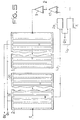
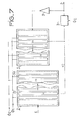
- FIGS 3 to 7 show various embodiments of the device according to the invention.
- the means of weighting P of the quantities of charges can be constituted by resistance bridges. They can also be constituted by weighting electrodes, inserted on each register with the transfer electrodes. Each weighting electrode is divided into at least two elementary electrodes separated according to the direction of charge transfer, by a cut-off and a weighted quantity of charges can be collected under each elementary electrode.
- the transfer and weighting electrodes ensure on periodic application of given potentials the transfer of charges in the substrate.
- the weighting means are constituted by weighting electrodes 20 interspersed with transfer electrodes 30 periodically receiving a potential ⁇ 1 ensuring the transfer of the charges in the substrate.
- each filter comprises two shift registers Rp and R N. Each register is assigned to the development of the weighting coefficients of the same sign, positive for Rp, and negative for R N.
- Each weighting electrode of the two registers 20 is divided into two elementary electrodes. A weighted amount of charge is collected under one of the elementary electrodes of the weighting electrodes of the two registers by two collection lines, Lp and L N , receiving quantities of weighted charge from a register of each filter.
- the two collection lines Lp and L N receive from each filter quantities of weighted charges to be assigned a weighting coefficient of the same sign, these lines are coupled to two devices for reading current or voltage loads Dp and D N.
- the means fixing the sign of the weighting coefficients and the means of algebraic summation of the quantities of weighted charges include a differential amplifier 17 of unity gain receiving on its inputs the signals coming from the reading.
- the device Dp is connected to the positive input and the device D N to the negative input of the differential amplifier.
- the potential ⁇ 2 is also applied to the other elementary electrodes, for example by means of the reading devices.
- each filter has a single register.
- Each weighting electrode 20 of the registers is divided into three elementary electrodes.
- a quantity of weighted charge is collected on two of the three elementary electrodes of each weighting electrode by the two collection lines Lp and L N.
- the elementary electrode of each weighting electrode under which charges are not collected has been placed, in the figure, between the two elementary electrodes under which charges are collected in order to allow easier extraction of the quantities of weighted charges. It is obvious that the respective positions of the three elementary electrodes can be modified.
- FIG. 4 makes it possible, compared with that of FIG. 3, to reduce the surface of the semiconductor used by reducing the number of registers. This decrease is even more important than the width of January 1 elementary electrode in which charges are not collected is lower. It may then be necessary to produce a broken line to connect to the potential cb2 the elementary electrodes under which charges are not collected.
- each filter has a single shift register.
- Each weighting electrode 20 is divided into two elementary electrodes. A weighted amount of charge is collected under one of the elementary electrodes by one or the other of the two collection lines, Lp and L N.
- the device of Figure 5 can only be used under certain conditions. Indeed, so that the charge transfer is not disturbed by the "edge effects", the dimension of an elementary electrode, in the direction perpendicular to that of the charge transfer or width, must not be less than a value limit d. In the devices of FIGS. 3 and 4, where the same number of coefficients of each sign is produced (some of them may be zero), each elementary electrode can be given a width d + x, the value x varying according to the weighting coefficient to be achieved. In the device of FIG. 5, where the number of coefficients of each sign varies with the transfer function to be performed, this is no longer possible.
- This embodiment makes it possible to reduce the stray capacitances reported by the elementary electrodes on the charge reading devices.
- the collection lines, Lp and L N can also receive from each filter quantities of weighted charges to be assigned weighting coefficients of different sign, the same sign as the input of the amplifier differential connected to the reading device coupled to the line, for the recursive filter and of opposite sign for the non-recursive filter.
- This embodiment has the advantage of reducing the number of inverters necessary for the looping of the recursive filter and above all makes it possible, in certain cases, to distribute the parasitic capacities reported on the reading devices by the elementary electrodes when there is' has imbalance between the values of the positive and negative weights.
- Figures 6 and 7 show two other embodiments of the device according to the invention in which the means of algebraic summation of the quantities of weighted charges are constituted by a single collection line L, receiving the weighted charges of the two filters.
- each filter comprises two registers Rp and R N.
- Each weighting electrode 20 is divided into two elementary electrodes. A weighted amount of charge is collected under one of the elementary electrodes of each weighting electrode by the collection line L.
- the means fixing the sign of the weighting coefficients are constituted by two inverters 18 and 19.
- the inverter 18 reverses the samples of the electrical input signal E to be filtered before they are applied to the means for injecting the charges 12 from the register R N , thus assigned to the development of the negative weighting coefficients, of the non-recursive filter 2.
- the inverter 19 reverses the electrical output signal S before it is applied to the means for injecting the charges 10 from the register Rp, thus assigned to the development of the positive weighting coefficients, of the recursive filter.
- the reading means are constituted by a charge reading device D, coupled to the collection line L and supplying the output signal S of the device.
- each filter has a single register.
- Each weighting electrode 20 is divided into two elementary electrodes. A weighted amount of charge is collected under one of the elementary electrodes of each weighting electrode by the collection line L.
- the means for reading the amounts of electrical charge and the means fixing the sign of the weighting coefficients are constituted by a device for reading loads D, single input and not phase shifting, coupled to the collection line and supplying the electrical output signal S of the device.
- each elementary electrode under which charges are not collected, for the purpose of reading periodically receives a given potential 4), which ensures the transfer of the charges in the substrate.
- This potential 4> 2 is also applied to the other elementary electrodes, for example by means of the reading device.
- the two filters 1 and 2 of the filtering device have the same structure. It is however understood that the invention relates to filtering devices of which at least one of the filters has the structure of the filters shown in FIGS. 3 to 5. The invention also relates to devices of which one of the filters is positive weighting coefficients and has a structure similar to that of the filters in Figure 7 and the other filter of which allows the development of positive and negative coefficients and requires two collection lines Lp and L N , two reading devices Dp and D N and a differential amplifier 17; the collection line of the positive coefficient filter is then coupled to the reading device connected to the positive input of the differential amplifier.
- the device according to the invention can be preceded by a pre-filtering device which makes it possible to select the frequency band containing the transfer function sought, since the device according to the invention has a periodic frequency response.
- Pre-filtering devices are known, for example by the article "Antialiasing inputs for charge couplet devices" by Carlo H. Seguin, published in the American review "IEEE Journal of Solid-State Circuits", volume SC 12, number 6 , December 1977, pages 609 to 616. This device can be placed, if we consider FIG. 2, between the charge injection device 12 of the non-recursive filter 2 and the first stage R 1 of the shift register.
Landscapes
- Solid State Image Pick-Up Elements (AREA)
- Filters That Use Time-Delay Elements (AREA)
- Networks Using Active Elements (AREA)
Claims (12)
Applications Claiming Priority (2)
| Application Number | Priority Date | Filing Date | Title |
|---|---|---|---|
| FR7828518 | 1978-10-05 | ||
| FR7828518A FR2438378A1 (fr) | 1978-10-05 | 1978-10-05 | Dispositif de filtrage a transfert de charges electriques |
Publications (2)
| Publication Number | Publication Date |
|---|---|
| EP0010039A1 EP0010039A1 (de) | 1980-04-16 |
| EP0010039B1 true EP0010039B1 (de) | 1983-03-30 |
Family
ID=9213386
Family Applications (1)
| Application Number | Title | Priority Date | Filing Date |
|---|---|---|---|
| EP79400693A Expired EP0010039B1 (de) | 1978-10-05 | 1979-09-28 | Filtervorrichtung mit einer Ladungsverschiebeanordnung |
Country Status (5)
| Country | Link |
|---|---|
| US (1) | US4264884A (de) |
| EP (1) | EP0010039B1 (de) |
| JP (1) | JPS5550723A (de) |
| DE (1) | DE2965115D1 (de) |
| FR (1) | FR2438378A1 (de) |
Families Citing this family (2)
| Publication number | Priority date | Publication date | Assignee | Title |
|---|---|---|---|---|
| JPS5827475A (ja) * | 1981-08-11 | 1983-02-18 | Hitachi Ltd | ゴ−スト除去装置 |
| US4387354A (en) * | 1981-08-31 | 1983-06-07 | Rca Corporation | CCD Triple-split gate electrode transversal filter |
Family Cites Families (4)
| Publication number | Priority date | Publication date | Assignee | Title |
|---|---|---|---|---|
| US3740591A (en) * | 1972-02-25 | 1973-06-19 | Gen Electric | Bucket-brigade tuned sampled data filter |
| FR2302636A1 (fr) * | 1975-02-28 | 1976-09-24 | Thomson Csf | Procede de filtrage de signaux analogiqu |
| US4100513A (en) * | 1975-09-18 | 1978-07-11 | Reticon Corporation | Semiconductor filtering apparatus |
| FR2394925A1 (fr) * | 1976-06-22 | 1979-01-12 | Thomson Csf | Filtre utilisant un dispositif a transfert de charges |
-
1978
- 1978-10-05 FR FR7828518A patent/FR2438378A1/fr active Granted
-
1979
- 1979-09-28 EP EP79400693A patent/EP0010039B1/de not_active Expired
- 1979-09-28 DE DE7979400693T patent/DE2965115D1/de not_active Expired
- 1979-10-03 US US06/081,456 patent/US4264884A/en not_active Expired - Lifetime
- 1979-10-04 JP JP12842979A patent/JPS5550723A/ja active Granted
Also Published As
| Publication number | Publication date |
|---|---|
| JPS6333730B2 (de) | 1988-07-06 |
| US4264884A (en) | 1981-04-28 |
| FR2438378A1 (fr) | 1980-04-30 |
| JPS5550723A (en) | 1980-04-12 |
| EP0010039A1 (de) | 1980-04-16 |
| DE2965115D1 (en) | 1983-05-05 |
| FR2438378B1 (de) | 1981-12-24 |
Similar Documents
| Publication | Publication Date | Title |
|---|---|---|
| EP0030173B1 (de) | Ladungsverschiebungsfilter mit geschalteten Kapazitäten | |
| EP0011556B1 (de) | Numerisch programmierbares Ladungsübertragungsfilter | |
| EP1053593B1 (de) | Resonatorfilter mit akustischen oberflächenwellen | |
| EP2131494B1 (de) | Schaltkreis mit geschalteten Kapazitäten mit geringem Energieverbrauch | |
| EP0010039B1 (de) | Filtervorrichtung mit einer Ladungsverschiebeanordnung | |
| FR2582461A1 (fr) | Filtre a decimation | |
| EP0006053A1 (de) | Differenzbildungsvorrichtung mit Ladungskopplung; Filter und Verzögerungsleitung mit einer solchen Vorrichtung | |
| EP0028961B1 (de) | Ladungsverschiebungsfilter und Filter mit geschalteten Kapazitäten versehen mit einem Vervielfacher mit geschalteten Kapazitäten | |
| FR2518848A1 (fr) | Systeme amplificateur comprenant un circuit de compensation de decalage | |
| EP0012667B1 (de) | Verfahren zum Filtern eines elektrischen Signals durch Ladungsübertragung in einem Halbleiter und Filter mit geschalteten Kondensatoren, das dieses Verfahren verwendet | |
| EP0207826A1 (de) | Detektorvorrichtung mit Zeitverzögerung und Integration in Phase | |
| EP0094265B1 (de) | Analog-numerischer Korrelator mit auf die Werte +1, -1 oder O programmierbaren Koeffizienten | |
| US4259597A (en) | Charge transfer signal processing apparatus | |
| EP0737002A1 (de) | CCD-Ausleseregister mit mehreren Ausgängen | |
| EP0129470B1 (de) | Festkörper photoempfindliche Anordnung | |
| EP0021908B1 (de) | Phasenumkehrschaltung mit Ladungsübertragung und Differenzverstärker mit solch einer Schaltung | |
| FR2626102A1 (fr) | Memoire a transfert de charges et procede de fabrication de cette memoire | |
| EP0011570B1 (de) | Die Ladungsübertragung in einem Halbleiter verwendende Filtervorrichtung | |
| EP0308287B1 (de) | Biquadratisches Element mit geschalteten Kapazitäten ohne stetige Gegenkopplung und mit niedriger Empfindlichkeit für die Verstärkung der Operationsverstärker und für das Verhältnis der Kapazitäten | |
| EP0076737A1 (de) | Symmetrischer Integrator und dessen Anwendung in einem Filter | |
| EP0011571A1 (de) | Rekursives Ladungsübertragungsfilter | |
| EP0143024B1 (de) | Mit geschalteten Kapazitäten durchgeführter exponentieller Integrator mit erhöhter Zeitkonstante | |
| EP0076195A1 (de) | Anordnung zur Stromauslesung einer Ladungsquantität und Ladungsübertragungsfilter mit solch einer Anordnung | |
| EP0226490B1 (de) | Synchrones Filter mit geschalteten Kapazitäten | |
| EP0633577B1 (de) | Retroaktiv gesteuerter Ladungs-Spannungsumsetzer |
Legal Events
| Date | Code | Title | Description |
|---|---|---|---|
| PUAI | Public reference made under article 153(3) epc to a published international application that has entered the european phase |
Free format text: ORIGINAL CODE: 0009012 |
|
| AK | Designated contracting states |
Designated state(s): DE GB NL |
|
| 17P | Request for examination filed | ||
| GRAA | (expected) grant |
Free format text: ORIGINAL CODE: 0009210 |
|
| AK | Designated contracting states |
Designated state(s): DE GB NL |
|
| REF | Corresponds to: |
Ref document number: 2965115 Country of ref document: DE Date of ref document: 19830505 |
|
| PGFP | Annual fee paid to national office [announced via postgrant information from national office to epo] |
Ref country code: GB Payment date: 19900813 Year of fee payment: 12 |
|
| PGFP | Annual fee paid to national office [announced via postgrant information from national office to epo] |
Ref country code: DE Payment date: 19900814 Year of fee payment: 12 |
|
| PGFP | Annual fee paid to national office [announced via postgrant information from national office to epo] |
Ref country code: NL Payment date: 19900930 Year of fee payment: 12 |
|
| PG25 | Lapsed in a contracting state [announced via postgrant information from national office to epo] |
Ref country code: GB Effective date: 19910928 |
|
| PG25 | Lapsed in a contracting state [announced via postgrant information from national office to epo] |
Ref country code: NL Effective date: 19920401 |
|
| NLV4 | Nl: lapsed or anulled due to non-payment of the annual fee | ||
| GBPC | Gb: european patent ceased through non-payment of renewal fee | ||
| PG25 | Lapsed in a contracting state [announced via postgrant information from national office to epo] |
Ref country code: DE Effective date: 19920602 |
|
| PLBE | No opposition filed within time limit |
Free format text: ORIGINAL CODE: 0009261 |
|
| STAA | Information on the status of an ep patent application or granted ep patent |
Free format text: STATUS: NO OPPOSITION FILED WITHIN TIME LIMIT |