EP0010462B1 - Vorrichtung zur Frequenz-Demodulation und eine solche Vorrichtung enthaltender Empfänger - Google Patents
Vorrichtung zur Frequenz-Demodulation und eine solche Vorrichtung enthaltender Empfänger Download PDFInfo
- Publication number
- EP0010462B1 EP0010462B1 EP79400653A EP79400653A EP0010462B1 EP 0010462 B1 EP0010462 B1 EP 0010462B1 EP 79400653 A EP79400653 A EP 79400653A EP 79400653 A EP79400653 A EP 79400653A EP 0010462 B1 EP0010462 B1 EP 0010462B1
- Authority
- EP
- European Patent Office
- Prior art keywords
- integration
- pass filter
- output
- input
- low
- Prior art date
- Legal status (The legal status is an assumption and is not a legal conclusion. Google has not performed a legal analysis and makes no representation as to the accuracy of the status listed.)
- Expired
Links
Images
Classifications
-
- H—ELECTRICITY
- H03—ELECTRONIC CIRCUITRY
- H03D—DEMODULATION OR TRANSFERENCE OF MODULATION FROM ONE CARRIER TO ANOTHER
- H03D3/00—Demodulation of angle-, frequency- or phase- modulated oscillations
- H03D3/02—Demodulation of angle-, frequency- or phase- modulated oscillations by detecting phase difference between two signals obtained from input signal
- H03D3/04—Demodulation of angle-, frequency- or phase- modulated oscillations by detecting phase difference between two signals obtained from input signal by counting or integrating cycles of oscillations
Definitions
- the present invention relates to devices for demodulating frequency modulated waves and in particular simple devices operating up to carrier frequencies of a few tens of megahertz.
- the limiter circuit clips the frequency modulated signal thus providing square frequency modulated signals from which the monostable flip-flop delivers pulses, of fixed and constant duration, from which the low-pass filter extracts the average value.
- the object of the present invention is to remedy this drawback.
- a demodulation device making it possible to demodulate frequency modulated signals, comprising amplitude limiting means receiving the signal to be demodulated, for transforming the signal to be demodulated in sequences of frequency modulated square or rectangular signals, coupled to a low-pass filter by means of integration means arranged between limiting means and the low-pass filter, is characterized in that the integration means integrate the output signals of the limiter according to a first constant d integration and up to a predetermined voltage value when the signal applied to their input has a first state and are reset to zero according to a second integration constant much lower than the first integration constant when the signal applied to their input has a second state, the voltage of predetermined value being such that the integration time is less than half the minimum period of the signal to be demodulated, the low-pass filter making it possible to extract the average value of the signal supplied by the integration means.
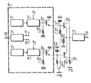
- a limiter circuit 6 receives on an input terminal 10, which is also the input of the demodulation device, signals to be demodulated.
- This circuit includes a resistor R 3 having a first terminal connected to a current source I through an electronic switch 3 controlled by a signal V 1 , and a second terminal connected to ground.
- the first terminal of this resistor R 3 is also connected to the base of a bipolar NPN transistor, Q 1 , whose collector is connected to ground and whose emitter constitutes a direct output of an amplitude limiting circuit 6
- a resistor R 4 has a first terminal connected to a current source 2 through an electronic switch 4 controlled by a signal V 2 , and a second terminal connected to ground.
- the first terminal of this resistor R 4 is also connected to the base of a bipolar NPN transistor, Q 2 , whose collector is connected to ground and whose emitter constitutes an inverted output of the amplitude limiting circuit 6.
- this amplitude limiting circuit 6 is an AM 685 comparator from Advanced Micro Devices whose input (+) receives the signal to be limited and whose input (-) is connected to the mass.
- the emitter of transistor Q 1 is connected to ground through an integrating capacitor C 1 , to a negative supply voltage V 4 through a resistor R 1 , and to the base of a bipolar transistor PNP whose l transmitter is connected to ground, through a resistor R 5 , and the collector of which is connected on the one hand to the output terminal 13, through a low-pass filter 5, and on the other hand to a voltage d negative supply V 3 through a resistor R s .
- the emitter of transistor O2 is connected to ground through an integrating capacitor C 2 , to voltage V 4 through a resistor R 2 , and to the base of a transistor Q 4 , whose emitter is connected to ground, through a resistor R 5 , and the collector of which is connected on the one hand to the output terminal 13, through the low-pass filter 5, and on the other hand to the supply voltage V 3 through the resistor R 6 .
- transistors Q 3 and Q 4 are chosen to be of the opposite type to that of the transistors Q 1 and Q 2 in order to reduce the temperature drifts of the device (compensation for the temperature drifts of the base-emitter voltages).
- the shaping circuit 7 delivers a voltage V 1 , on its output terminal 11, and makes it possible to close the switch 3, and a voltage V 2 of zero value which leaves switch 4 open. Conversely when the value of the input voltage applied to terminal 10 is negative, switch 4 is closed and switch 3 is open.
- This capacitor C 1 would charge until the value of the voltage across its terminals is equal to -V 4 but for a value of this voltage equal to -R 3 . l o -V BE the transistor Q 1 begins to conduct (V BE being the voltage between the base and the emitter of this transistor) and the voltage across the capacitor C 1 remains blocked at this latter value.
- the value of the voltage -V 4 is very large in absolute value compared to the voltage -R 3 . l o -V BE , which allows a quasi-linear charge of the capacitor C 1 .
- the transistor Q 3 connected as a common emitter transmits these voltage variations to the output 13 through the low-pass filter 5 by reversing the phase of these voltage variations and by amplifying them.
- the signals of these two sets are summed in the common load of collector of the transistors Q 3 and Q 4 then filtered by the low-pass filter 5 which makes it possible to extract their average value from it.
- the summation, which is not essential, of the two channels makes it possible to double the value of the amplitude of the demodulated signal, but also to double the value of the different frequencies which must be eliminated by the low-pass filter. 5, which ultimately eases the filtering problem.
- this device therefore constitutes a frequency demodulator.
- the low-pass filter 5 can be connected to the coupled emitters of the transistors Q 3 and Q 4 .
- Such devices can be used in particular in frequency modulation receivers.
Landscapes
- Engineering & Computer Science (AREA)
- Power Engineering (AREA)
- Digital Transmission Methods That Use Modulated Carrier Waves (AREA)
- Superheterodyne Receivers (AREA)
- Circuits Of Receivers In General (AREA)
- Networks Using Active Elements (AREA)
Claims (6)
Applications Claiming Priority (2)
| Application Number | Priority Date | Filing Date | Title |
|---|---|---|---|
| FR7827917A FR2437732A1 (fr) | 1978-09-29 | 1978-09-29 | Dispositif de demodulation de frequence et recepteur comportant un tel dispositif |
| FR7827917 | 1978-09-29 |
Publications (2)
| Publication Number | Publication Date |
|---|---|
| EP0010462A1 EP0010462A1 (de) | 1980-04-30 |
| EP0010462B1 true EP0010462B1 (de) | 1984-06-20 |
Family
ID=9213179
Family Applications (1)
| Application Number | Title | Priority Date | Filing Date |
|---|---|---|---|
| EP79400653A Expired EP0010462B1 (de) | 1978-09-29 | 1979-09-18 | Vorrichtung zur Frequenz-Demodulation und eine solche Vorrichtung enthaltender Empfänger |
Country Status (4)
| Country | Link |
|---|---|
| US (1) | US4303888A (de) |
| EP (1) | EP0010462B1 (de) |
| DE (1) | DE2967066D1 (de) |
| FR (1) | FR2437732A1 (de) |
Families Citing this family (2)
| Publication number | Priority date | Publication date | Assignee | Title |
|---|---|---|---|---|
| US7477100B2 (en) * | 2004-04-27 | 2009-01-13 | Broadcom Corporation | Method and system for single ended to differential ended demodulation |
| US8216323B2 (en) | 2005-06-30 | 2012-07-10 | General Electric Company | System and method for hydrogen production |
Family Cites Families (8)
| Publication number | Priority date | Publication date | Assignee | Title |
|---|---|---|---|---|
| GB985205A (en) * | 1961-12-18 | 1965-03-03 | British Telecomm Res Ltd | Improvements in demodulator circuits for frequency modulated electrical signals |
| US3320434A (en) * | 1964-01-09 | 1967-05-16 | Data Control Systems Inc | Generator producing controlledarea output-pulses only when capacitor charges between positive and negative clamps in response to a.c. input |
| US3407358A (en) * | 1964-12-07 | 1968-10-22 | Data Control Systems Inc | Apparatus for demodulating an fm carrier |
| FR1468911A (fr) * | 1965-11-12 | 1967-02-10 | Snecma | Convertisseur analogique et son application à la régulation |
| US3473133A (en) * | 1966-12-30 | 1969-10-14 | Motorola Inc | Pulse counter detector |
| US3614634A (en) * | 1969-09-02 | 1971-10-19 | Texas Instruments Inc | Frequency conversion system |
| US3723891A (en) * | 1971-05-12 | 1973-03-27 | Us Navy | Frequency to voltage converter |
| CH549217A (de) * | 1972-09-09 | 1974-05-15 | Egloff Adolf | Verfahren und einrichtung zur umwandlung einer elektrischen wechselspannung in eine frequenzproportionale gleichspannung. |
-
1978
- 1978-09-29 FR FR7827917A patent/FR2437732A1/fr active Granted
-
1979
- 1979-09-18 EP EP79400653A patent/EP0010462B1/de not_active Expired
- 1979-09-18 DE DE7979400653T patent/DE2967066D1/de not_active Expired
- 1979-09-25 US US06/078,803 patent/US4303888A/en not_active Expired - Lifetime
Also Published As
| Publication number | Publication date |
|---|---|
| DE2967066D1 (en) | 1984-07-26 |
| FR2437732B1 (de) | 1981-09-11 |
| EP0010462A1 (de) | 1980-04-30 |
| FR2437732A1 (fr) | 1980-04-25 |
| US4303888A (en) | 1981-12-01 |
Similar Documents
| Publication | Publication Date | Title |
|---|---|---|
| EP0778669B1 (de) | Frequenzdemodulator | |
| FR2622751A1 (fr) | Circuit modulateur/demodulateur et amplificateur d'isolation employant ce circuit | |
| EP0048661B1 (de) | Demodulator eines frequenzmodulierten Signals | |
| FR2472312A1 (fr) | Recepteur a superreaction | |
| US4618967A (en) | Radio receiver | |
| FR2473816A1 (fr) | Systeme a blocage de boucle | |
| FR2546001A1 (fr) | Demodulateur de signaux, a enveloppe constante et phase continue, modules angulairement par un train de symboles binaires | |
| FR2563669A1 (fr) | Circuit integrable destine a commander la vitesse de la variation de la tension de dispositifs de commutation commandes par tension, au moment du blocage | |
| FR2503496A1 (fr) | Circuit detecteur de bruit et recepteur de signal pour un recepteur a modulation de frequence | |
| EP0010462A1 (de) | Vorrichtung zur Frequenz-Demodulation und eine solche Vorrichtung enthaltender Empfänger | |
| US4140928A (en) | Monostable multivibrator | |
| EP0055670A2 (de) | Schaltung zur Regelung des Tastverhältnisses eines periodischen Impulssignals und 2n-Frequenzvervielfacher mit dieser Regelschaltung | |
| US4247823A (en) | Low noise, low phase shift analog signal multiplier | |
| FR2485294A1 (fr) | Demodulateur de frequence utilisant un circuit a retard variable avec la frequence recue | |
| FR2509502A1 (fr) | Dispositif de reproduction magnetique pour signal numerique | |
| FR2542529A1 (fr) | Circuit de reduction des bruits d'impulsions par interpolation lineaire avec insensibilite aux bruits blancs | |
| EP0046421B1 (de) | Empfänger für Signalübertragungssystem mittels elektromagnetischer, insbesondere infraroter Strahlung | |
| JPS6190516A (ja) | 位相比較回路 | |
| FR2602104A1 (fr) | Dispositif de modulation de frequence a correction statique de linearite et emetteur comportant un tel dispositif | |
| EP1648084B1 (de) | Mischerschaltung | |
| FR2458959A1 (fr) | Emetteur electronique pour des systemes de telegraphie par courant continu | |
| EP0031746A2 (de) | Schaltung zur Demodulation eines digital modulierten Signals und eine solche Schaltung enthaltender Empfänger | |
| FR2546005A1 (fr) | Perfectionnements concernant les quantificateurs de donnees | |
| FR2486339A1 (fr) | Detecteur synchrone | |
| SU866754A1 (ru) | Приемник частотно-манипулированных сигналов |
Legal Events
| Date | Code | Title | Description |
|---|---|---|---|
| PUAI | Public reference made under article 153(3) epc to a published international application that has entered the european phase |
Free format text: ORIGINAL CODE: 0009012 |
|
| AK | Designated contracting states |
Designated state(s): DE GB |
|
| 17P | Request for examination filed |
Effective date: 19800714 |
|
| GRAA | (expected) grant |
Free format text: ORIGINAL CODE: 0009210 |
|
| RBV | Designated contracting states (corrected) |
Designated state(s): DE GB |
|
| AK | Designated contracting states |
Designated state(s): DE GB |
|
| PGFP | Annual fee paid to national office [announced via postgrant information from national office to epo] |
Ref country code: DE Payment date: 19840723 Year of fee payment: 6 |
|
| REF | Corresponds to: |
Ref document number: 2967066 Country of ref document: DE Date of ref document: 19840726 |
|
| PLBE | No opposition filed within time limit |
Free format text: ORIGINAL CODE: 0009261 |
|
| STAA | Information on the status of an ep patent application or granted ep patent |
Free format text: STATUS: NO OPPOSITION FILED WITHIN TIME LIMIT |
|
| 26N | No opposition filed | ||
| PG25 | Lapsed in a contracting state [announced via postgrant information from national office to epo] |
Ref country code: DE Effective date: 19870602 |
|
| GBPC | Gb: european patent ceased through non-payment of renewal fee | ||
| PG25 | Lapsed in a contracting state [announced via postgrant information from national office to epo] |
Ref country code: GB Effective date: 19881118 |