EP0011406B1 - Carte de circuit imprimé à couches multiples et procédé pour sa fabrication - Google Patents
Carte de circuit imprimé à couches multiples et procédé pour sa fabrication Download PDFInfo
- Publication number
- EP0011406B1 EP0011406B1 EP79302335A EP79302335A EP0011406B1 EP 0011406 B1 EP0011406 B1 EP 0011406B1 EP 79302335 A EP79302335 A EP 79302335A EP 79302335 A EP79302335 A EP 79302335A EP 0011406 B1 EP0011406 B1 EP 0011406B1
- Authority
- EP
- European Patent Office
- Prior art keywords
- multilayer circuit
- glass
- circuit board
- insulator
- alumina
- Prior art date
- Legal status (The legal status is an assumption and is not a legal conclusion. Google has not performed a legal analysis and makes no representation as to the accuracy of the status listed.)
- Expired
Links
Images


Classifications
-
- H—ELECTRICITY
- H05—ELECTRIC TECHNIQUES NOT OTHERWISE PROVIDED FOR
- H05K—PRINTED CIRCUITS; CASINGS OR CONSTRUCTIONAL DETAILS OF ELECTRIC APPARATUS; MANUFACTURE OF ASSEMBLAGES OF ELECTRICAL COMPONENTS
- H05K3/00—Apparatus or processes for manufacturing printed circuits
- H05K3/46—Manufacturing multilayer circuits
- H05K3/4644—Manufacturing multilayer circuits by building the multilayer layer by layer, i.e. build-up multilayer circuits
- H05K3/4664—Adding a circuit layer by thick film methods, e.g. printing techniques or by other techniques for making conductive patterns by using pastes, inks or powders
-
- H—ELECTRICITY
- H10—SEMICONDUCTOR DEVICES; ELECTRIC SOLID-STATE DEVICES NOT OTHERWISE PROVIDED FOR
- H10W—GENERIC PACKAGES, INTERCONNECTIONS, CONNECTORS OR OTHER CONSTRUCTIONAL DETAILS OF DEVICES COVERED BY CLASS H10
- H10W70/00—Package substrates; Interposers; Redistribution layers [RDL]
- H10W70/60—Insulating or insulated package substrates; Interposers; Redistribution layers
- H10W70/611—Insulating or insulated package substrates; Interposers; Redistribution layers for connecting multiple chips together
-
- H—ELECTRICITY
- H10—SEMICONDUCTOR DEVICES; ELECTRIC SOLID-STATE DEVICES NOT OTHERWISE PROVIDED FOR
- H10W—GENERIC PACKAGES, INTERCONNECTIONS, CONNECTORS OR OTHER CONSTRUCTIONAL DETAILS OF DEVICES COVERED BY CLASS H10
- H10W70/00—Package substrates; Interposers; Redistribution layers [RDL]
- H10W70/60—Insulating or insulated package substrates; Interposers; Redistribution layers
- H10W70/67—Insulating or insulated package substrates; Interposers; Redistribution layers characterised by their insulating layers or insulating parts
- H10W70/68—Shapes or dispositions thereof
- H10W70/685—Shapes or dispositions thereof comprising multiple insulating layers
-
- H—ELECTRICITY
- H10—SEMICONDUCTOR DEVICES; ELECTRIC SOLID-STATE DEVICES NOT OTHERWISE PROVIDED FOR
- H10W—GENERIC PACKAGES, INTERCONNECTIONS, CONNECTORS OR OTHER CONSTRUCTIONAL DETAILS OF DEVICES COVERED BY CLASS H10
- H10W70/00—Package substrates; Interposers; Redistribution layers [RDL]
- H10W70/60—Insulating or insulated package substrates; Interposers; Redistribution layers
- H10W70/67—Insulating or insulated package substrates; Interposers; Redistribution layers characterised by their insulating layers or insulating parts
- H10W70/69—Insulating materials thereof
- H10W70/692—Ceramics or glasses
Definitions
- the present invention relates to a multilayer circuit board which has a predetermined characteristic impedance and on which large scale integration devices (LSls) are mounted.
- LSls large scale integration devices
- a multilayer circuit board on which such semiconductor devices generating heat are mounted should have the following requirements:-
- a multilayer circuit board has been previously produced by two methods: (1) a laminating method; and, (2) a thick film printing method.
- powdered ceramic material e.g. AI 2 0 3
- organic binder e.g. N-(2-aminoethyl)
- green sheets e.g. N-(2-aminoethyl)
- metal paste for a conductor circuit
- All the green sheets are laminated together and then sintered at an elevated temperature of 1350-1600°C to produce a multilayer laminated ceramic board.
- the multilayer laminated ceramic board produced by this method has the following disadvantages:-
- a paste for the conductor layers e.g. a paste of Silver, Gold or Copper and a paste for insulating material e.g. a paste of glass, crystalline glass or glass-ceramic are alternately printed on to a fired ceramic plate by a screen printing method to form an unfired multilayer circuit board. Then, the board is fired at a temperature of 700 to 1000°C to produce a finished article.
- the multilayer circuit board produced by this method has the following disadvantages:
- a multilayer circuit board comprises a first multilayer circuit including a ground conductor surrounded by an insulator, a second multilayer circuit including signal conductors surrounded by an insulator, and a central insulating layer between the first and said second multilayer circuits, the central insulating layer being made of insulating material having a larger thermal conductivity than that of the insulator in the first and second multilayer circuits and having a larger dielectric constant than that of the insulator in the first and second multilayer circuits.
- the present invention results in an improved multilayer circuit board which has a smaller signal propagation delay and better thermal dissipating properties compared to previous multilayer circuit boards. It also results in a multilayer circuit board which has a predetermined characteristic impedance and which is thinner than previous multilayer circuit boards.
- the first multilayer circuit also includes a supply voltage conductor.
- the insulator in the first and second multilayer circuits in a glass-ceramic consisting of borosilicate glass and alumina and having a low dielectric constant, and the central insulating layer is sintered alumina plate.
- the dielectric constant of the insulator surrounding a signal conductor influences the signal propagation delay
- Gold, Silver, Copper or an alloy thereof is a material for the conductors, since the electric resistance of these metals is low and the melting points of these metals are higher than the firing temperature (approximately 900°C) for the glass-ceramic material.
- borosilicate glass is suitable for the glass of a glass-ceramic insulating material, taking the following requirements into consideration.
- alumina is suitable for the ceramic material of a glass-ceramic insulating material, taking the following requirements into consideration.
- Glass-ceramic is produced by mixing borosilicate glass powder, alumina powder and a binder to form a paste, by forming an insulating layer of the paste by means of a screen process printing and then by firing the paste.
- the grain size of the alumina powder affects the density of the glass-ceramic.
- Fig. 1 shows a relationship between the glass content of glass-ceramic and the optimum firing temperature. It is clear from Fig. 1 that the optimum firing temperature, i.e.
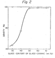
- Fig. 2 shows a relationship between the glass-content of glass-ceramic and the density of glass-ceramic at the optimum firing temperature. It is clear from Fig. 2 that at least 50 wt% of the glass content can ensure a high density of the glass-ceramic.
- Figs. 3 and 4 show a relationship between the glass content,of glass-ceramic and the dielectric constant and a relationship between the glass content of glass-ceramic and the thermal conductivity, respectively. It is clear from Fig. 3 and 4. that the dielectric constant and the thermal conductivity is decreased as the glass content increases.
- the thermal expansion coefficient and the flexural strength of glass-ceramic are reduced as the glass content of the glass-ceramic increases.
- the most preferable glass-ceramic consisted of 50 wt% of borosilicate glass having the composition of Sample 1 in Table 1 and 50 wt% of alumina and was fired at approximately 900°C. Concerning the firing time, in this case at the temperature of 900°C, it was found that the density of glass-ceramic could be increased to a high level by firing for at least 5 minutes and that the obtained high level density was hardly increased by continuing the firing for some hours.
- the most preferable glass-ceramic has properties indicated in Table 2.
- the thermal expansion coefficient of the glass-ceramic is near that of single crystalline silicon, which is used as a substrate of a semiconductor device and is fixed on the surface of the glass-ceramic. Accordingly, stress generated in contacting parts of the glass-ceramic and silicon substrate by the difference between the thermal expansion coefficient is small.
- an alumina sintered plate is made of alumina (Al 2 O 3 ) having a purity of more than 90% and having a density of more than 95%, taking the following facts into consideration.
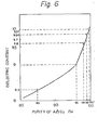
- Figs. 5 and 6 show the relationship between the purity of Al 2 O 3 and the thermal conductivity of an alumina sintered plate and the relationship between the purity of A1 2 0 3 and the dielectric constant, respectively. Taking the requirements for an alumina sintered plate in a multilayer circuit board and Figs. 5 and 6 into consideration, the purity of Al z 0 3 should not be less than 90%. Furthermore, Fig. 7 shows the relationship between sintered density and thermal conductivity of an alumina sintered plate made of alumina having a purity of 99.7%. Since alumina sintered plates having a density of less than 95% had some degree of water absorption, an alumina sintered plate to be used for the multilayer circuit board of the present invention needs a density of more than 95%.
- a thermal expansion coefficient of the glass-ceramic is smaller than that of the alumina sintered plate, such a difference of the thermal expansion coefficient may generate a camber of a multilayer circuit board.
- the generation of a camber can be prevented by forming the same thickness of the glass-ceramic layers on both surfaces of the alumina sintered plate.
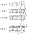
- Figs. 8a through 8h are schematic, cross-sectional views of a multilayer circuit board according to the present invention in various stages of its production.
- glass-ceramic paste layers 2, 2' were entirely applied by means of a conventional screen process printing and then fired at 900°C for 10 minutes to form glass-ceramic layers 2, 2' being 25 ⁇ m thick.
- the alumina sintered plate used was 80 mm wide, 80 mm long and 0.60 mm thick and was made of a purity of 99.7% of alumina.
- the glass-ceramic paste used was produced by mixing borosilicate glass powder and alumina powder in the ratio of 51 :49 (weight), adding a binder and a solvent indicated in Table 3 at a ratio of 94 g per 100 g of the mixed powder into the mixed powder, mixing them for approximately 20 hours and then evaporating methyl ethyl ketone. Since the above mixing was carried out in a ball mill in which alumina balls are contained, the weight ratio of the glass powder and the alumina powder in the obtained paste became 1:1.
- the borosilicate glass powder used had a grain size of 325 mesh and a composition of Sample 1 indicated in Table 1.
- the alumina powder used had an average grain size of 3.5 ⁇ m and a purity of 99.7%.
- Holes 3 i.e. via holes
- the holes 3 made had a diameter of 100 pm.
- the holes 3 were filled with gold (Au) conductor paste 4 and then the paste 4 was fired at 900°C for 10 minutes.
- the Au conductor paste used was produced by adding the borosilicate glass of Sample 1 of 2 wt% into commercial 99% Au paste. The addition of borosilicate glass was carried out in order to increase the bond strength between the Au conductor being formed and the alumina sintered plate or the glass-ceramic.
- Layers 5, 5' of the above-mentioned Au conductor paste were applied on both entire surfaces of the formed glass-ceramic layers 2, 2' by means of a screen process printing and then fired at 900°C for 10 minutes. As a result, conductor layers 5, 5' being 15 ⁇ m thick were formed.
- the formed conductor layers 5, 5' were etched by a conventional photo etching process to form conductor circuits 6, 6' having a conductor width of 50 m and a conductor spacing of 50 ⁇ m.
- positive type photo resist and etchant containing potassium iodide-iodine (Kl ⁇ l 2 ) were used.
- the glass-ceramic paste described in Stage 1 was applied on both entire surfaces of the formed conductor circuits 6, 6' and the formed glass-ceramic layers 2, 2' by' means of the screen process printing method and then fired at 900°C for 10 minutes to form glass-ceramic layers 7, 7' being 25 ⁇ m thick (on the conductor). It is possible to form glass-ceramic layers 7, 7' by repeating the application and the firing of the glass-ceramic paste two times. In this case, the first firing time may be 1-2 minutes.
- the formed glass-ceramic layers 7, 7' were etched by a conventional photo etching process to make via holes 8, 8' having a diameter of 100 ⁇ m.
- the etching was carried out by using a negative type photo resist and an etchant containing hydrogen fluoride-sulphuric acid (HF ⁇ H 2 SO 4 ).
- Stages 3 through 7 were repeated to produce a multilayer circuit board 10 (Fig. 8h) having seven conductor layers.
- the seven conductor layers consisted of four signal layers 60, one surface layer 61, one ground layer 62 and one supply voltage layer 63.
- the conductor thus formed had an electric resistance of 500 m ⁇ /cm.
- the latter board was produced by the above mentioned laminating method.
- the latter board consisted of ceramic made of alumina having a purity of 92% and seven conductor layers made of tungsten (W) therein.
- the properties (characteristic impedance, signal propagation delay and thermal resistance) of the multilayer circuit boards according to the present invention and the prior art can be calculated from the following equations (1) (2) and (3) by substituting the values indicated in Tables 4 and 5 into the equations.
- the multilayer circuit board of the present invention has a small signal propagation delay and a better heat dissipation property (i.e. a thinner board thickness and a smaller thermal resistance) as compared with the multilayer circuit board having the same width and length as those of the former board produced by the laminating method of the prior art.
Landscapes
- Engineering & Computer Science (AREA)
- Manufacturing & Machinery (AREA)
- Microelectronics & Electronic Packaging (AREA)
- Production Of Multi-Layered Print Wiring Board (AREA)
- Laminated Bodies (AREA)
Claims (9)
Applications Claiming Priority (2)
| Application Number | Priority Date | Filing Date | Title |
|---|---|---|---|
| JP137710/78 | 1978-11-08 | ||
| JP13771078A JPS5563900A (en) | 1978-11-08 | 1978-11-08 | Multilyaer ceramic circuit board |
Publications (2)
| Publication Number | Publication Date |
|---|---|
| EP0011406A1 EP0011406A1 (fr) | 1980-05-28 |
| EP0011406B1 true EP0011406B1 (fr) | 1982-11-03 |
Family
ID=15205004
Family Applications (1)
| Application Number | Title | Priority Date | Filing Date |
|---|---|---|---|
| EP79302335A Expired EP0011406B1 (fr) | 1978-11-08 | 1979-10-25 | Carte de circuit imprimé à couches multiples et procédé pour sa fabrication |
Country Status (4)
| Country | Link |
|---|---|
| US (1) | US4313026A (fr) |
| EP (1) | EP0011406B1 (fr) |
| JP (1) | JPS5563900A (fr) |
| DE (1) | DE2963987D1 (fr) |
Families Citing this family (37)
| Publication number | Priority date | Publication date | Assignee | Title |
|---|---|---|---|---|
| US4376725A (en) * | 1980-10-17 | 1983-03-15 | Rca Corporation | Conductor inks |
| JPS57115896A (en) * | 1981-01-10 | 1982-07-19 | Nippon Electric Co | High density integrated circuit board |
| US4628149A (en) * | 1981-11-30 | 1986-12-09 | Nippon Electric Co., Ltd. | Substrate having a pattern of an alloy of gold and a noble and a base metal with the pattern isolated by oxides of the noble and the base metals |
| JPS599992A (ja) * | 1982-07-08 | 1984-01-19 | 株式会社日立製作所 | 多層配線基板の製造方法 |
| JPS5911700A (ja) * | 1982-07-12 | 1984-01-21 | 株式会社日立製作所 | セラミツク多層配線回路板 |
| US4498122A (en) * | 1982-12-29 | 1985-02-05 | At&T Bell Laboratories | High-speed, high pin-out LSI chip package |
| JPS6028296A (ja) * | 1983-07-27 | 1985-02-13 | 株式会社日立製作所 | セラミツク多層配線回路板 |
| JPS60221358A (ja) * | 1984-04-13 | 1985-11-06 | 日本碍子株式会社 | 電気絶縁体用セラミック組成物 |
| US4943470A (en) * | 1985-01-11 | 1990-07-24 | Ngk Spark Plug Co., Ltd. | Ceramic substrate for electrical devices |
| US4712161A (en) * | 1985-03-25 | 1987-12-08 | Olin Corporation | Hybrid and multi-layer circuitry |
| US4840654A (en) * | 1985-03-04 | 1989-06-20 | Olin Corporation | Method for making multi-layer and pin grid arrays |
| JPS61158423U (fr) * | 1985-03-22 | 1986-10-01 | ||
| US4696851A (en) * | 1985-03-25 | 1987-09-29 | Olin Corporation | Hybrid and multi-layer circuitry |
| JPS61229389A (ja) * | 1985-04-03 | 1986-10-13 | イビデン株式会社 | セラミツク配線板およびその製造方法 |
| JPH0634452B2 (ja) * | 1985-08-05 | 1994-05-02 | 株式会社日立製作所 | セラミツクス回路基板 |
| JPS6247196A (ja) * | 1985-08-26 | 1987-02-28 | 松下電器産業株式会社 | セラミツク多層基板 |
| US4725333A (en) * | 1985-12-20 | 1988-02-16 | Olin Corporation | Metal-glass laminate and process for producing same |
| US4687540A (en) * | 1985-12-20 | 1987-08-18 | Olin Corporation | Method of manufacturing glass capacitors and resulting product |
| US4821151A (en) * | 1985-12-20 | 1989-04-11 | Olin Corporation | Hermetically sealed package |
| JPS62265796A (ja) * | 1986-05-14 | 1987-11-18 | 株式会社住友金属セラミックス | セラミツク多層配線基板およびその製造法 |
| US5102749A (en) * | 1988-01-27 | 1992-04-07 | W. R. Grace & Co.-Conn. | Electronic package comprising aluminum nitride and aluminum nitride-borosilicate glass composite |
| US5017434A (en) * | 1988-01-27 | 1991-05-21 | Enloe Jack H | Electronic package comprising aluminum nitride and aluminum nitride-borosilicate glass composite |
| US4882454A (en) * | 1988-02-12 | 1989-11-21 | Texas Instruments Incorporated | Thermal interface for a printed wiring board |
| US4963697A (en) * | 1988-02-12 | 1990-10-16 | Texas Instruments Incorporated | Advanced polymers on metal printed wiring board |
| US5346751A (en) * | 1988-12-19 | 1994-09-13 | W. R. Grace & Co.-Conn. | Electronic package using closed pore composites |
| US5082804A (en) * | 1989-01-19 | 1992-01-21 | David Sarnoff Research Center, Inc. | Thick film copper via fill inks |
| JP3520540B2 (ja) * | 1993-12-07 | 2004-04-19 | 株式会社デンソー | 多層基板 |
| US5849396A (en) * | 1995-09-13 | 1998-12-15 | Hughes Electronics Corporation | Multilayer electronic structure and its preparation |
| IT1286786B1 (it) * | 1996-11-25 | 1998-07-17 | Sicis Int Srl | Procedimento per la fabbricazione di lastre di vetro e oro per mosaico |
| US6286204B1 (en) * | 1998-03-09 | 2001-09-11 | Sarnoff Corporation | Method for fabricating double sided ceramic circuit boards using a titanium support substrate |
| JP2000244123A (ja) * | 1999-02-19 | 2000-09-08 | Hitachi Ltd | 多層セラミック回路基板 |
| JP3601679B2 (ja) * | 1999-07-27 | 2004-12-15 | 株式会社村田製作所 | 複合積層体の製造方法 |
| JP3669219B2 (ja) * | 1999-08-10 | 2005-07-06 | 日本電気株式会社 | 多層プリント配線板 |
| JP3554962B2 (ja) * | 1999-10-28 | 2004-08-18 | 株式会社村田製作所 | 複合積層体およびその製造方法 |
| US6519313B2 (en) * | 2001-05-30 | 2003-02-11 | General Electric Company | High-Z cast reflector compositions and method of manufacture |
| US7132743B2 (en) * | 2003-12-23 | 2006-11-07 | Intel Corporation | Integrated circuit package substrate having a thin film capacitor structure |
| US20080157335A1 (en) * | 2006-12-28 | 2008-07-03 | Jia Miao Tang | Strip patterned transmission line |
Family Cites Families (9)
| Publication number | Priority date | Publication date | Assignee | Title |
|---|---|---|---|---|
| US2885826A (en) * | 1954-12-21 | 1959-05-12 | British Thomson Houston Co Ltd | Glass-to-metal seals |
| US3200298A (en) * | 1963-05-27 | 1965-08-10 | United Aircraft Corp | Multilayer ceramic circuitry |
| US3312870A (en) * | 1964-03-13 | 1967-04-04 | Hughes Aircraft Co | Electrical transmission system |
| US3423517A (en) * | 1966-07-27 | 1969-01-21 | Dielectric Systems Inc | Monolithic ceramic electrical interconnecting structure |
| US3549784A (en) * | 1968-02-01 | 1970-12-22 | American Lava Corp | Ceramic-metallic composite substrate |
| US3723176A (en) * | 1969-06-19 | 1973-03-27 | American Lava Corp | Alumina palladium composite |
| US3676087A (en) * | 1971-03-15 | 1972-07-11 | Bell Telephone Labor Inc | Technique for the fabrication of a photolithographically definable,glass covered gold conductor pattern |
| US3958377A (en) * | 1974-06-25 | 1976-05-25 | Milner Jr Edwin Earl | Lightweight high strength boom construction |
| GB1501500A (en) * | 1975-06-20 | 1978-02-15 | Int Computers Ltd | Multilayer printed circuit boards |
-
1978
- 1978-11-08 JP JP13771078A patent/JPS5563900A/ja active Granted
-
1979
- 1979-10-25 EP EP79302335A patent/EP0011406B1/fr not_active Expired
- 1979-10-25 DE DE7979302335T patent/DE2963987D1/de not_active Expired
- 1979-10-26 US US06/088,467 patent/US4313026A/en not_active Expired - Lifetime
Also Published As
| Publication number | Publication date |
|---|---|
| JPS5719599B2 (fr) | 1982-04-23 |
| JPS5563900A (en) | 1980-05-14 |
| EP0011406A1 (fr) | 1980-05-28 |
| DE2963987D1 (en) | 1982-12-09 |
| US4313026A (en) | 1982-01-26 |
Similar Documents
| Publication | Publication Date | Title |
|---|---|---|
| EP0011406B1 (fr) | Carte de circuit imprimé à couches multiples et procédé pour sa fabrication | |
| KR930000881B1 (ko) | 세라믹 다층 회로판 및 반도체 모듈 | |
| US4827083A (en) | Wiring substrate | |
| JP2924177B2 (ja) | 傾斜機能型回路用基板 | |
| US5099388A (en) | Alumina multilayer wiring substrate provided with high dielectric material layer | |
| US4618590A (en) | Starting mixture for a dielectric composition | |
| US5292574A (en) | Ceramic substrate having wiring of silver series | |
| US5122930A (en) | High heat-conductive, thick film multi-layered circuit board | |
| US6037045A (en) | Thick-film paste and ceramic circuit substrate using the same | |
| JPH0447978B2 (fr) | ||
| JP3473891B2 (ja) | 高周波インダクタの製造方法 | |
| US4927711A (en) | Hybrid circuits and thick film dielectrics used therein | |
| US5903429A (en) | Capacitor, method for producing same and method for producing dielectric body | |
| KR19990067290A (ko) | 다층 공-소성 세라믹 조성물 및 금속상-세라믹 회로판 | |
| Barnwell et al. | A novel thick film on ceramic MCM technology offering MCM-D performance | |
| JP2001127224A (ja) | 絶縁性アルミナ質基板およびアルミナ質銅貼回路基板 | |
| JPH029473B2 (fr) | ||
| KR830000829B1 (ko) | 다층의 세라믹 회로 기판 | |
| Dummer | Integrated electronics ߞa historical introduction | |
| JP2752301B2 (ja) | セラミック基板用組成物及びセラミック配線基板 | |
| Minalgiene et al. | Very fine line photoimageable thick film technology developed at hibridas | |
| JPH01120096A (ja) | 多層回路基板 | |
| JPS60171781A (ja) | 低誘電率多層基板の製造方法 | |
| Sergent | ‘‘‘Ceramics and Ceramic Composites | |
| JPH06232528A (ja) | 混成集積回路基板及びその製法 |
Legal Events
| Date | Code | Title | Description |
|---|---|---|---|
| PUAI | Public reference made under article 153(3) epc to a published international application that has entered the european phase |
Free format text: ORIGINAL CODE: 0009012 |
|
| 17P | Request for examination filed | ||
| AK | Designated contracting states |
Designated state(s): DE FR GB IT NL |
|
| ITF | It: translation for a ep patent filed | ||
| GRAA | (expected) grant |
Free format text: ORIGINAL CODE: 0009210 |
|
| AK | Designated contracting states |
Designated state(s): DE FR GB IT NL |
|
| REF | Corresponds to: |
Ref document number: 2963987 Country of ref document: DE Date of ref document: 19821209 |
|
| ET | Fr: translation filed | ||
| PGFP | Annual fee paid to national office [announced via postgrant information from national office to epo] |
Ref country code: GB Payment date: 19921015 Year of fee payment: 14 |
|
| PGFP | Annual fee paid to national office [announced via postgrant information from national office to epo] |
Ref country code: FR Payment date: 19921028 Year of fee payment: 14 |
|
| ITTA | It: last paid annual fee | ||
| PGFP | Annual fee paid to national office [announced via postgrant information from national office to epo] |
Ref country code: NL Payment date: 19921031 Year of fee payment: 14 |
|
| PGFP | Annual fee paid to national office [announced via postgrant information from national office to epo] |
Ref country code: DE Payment date: 19921127 Year of fee payment: 14 |
|
| PG25 | Lapsed in a contracting state [announced via postgrant information from national office to epo] |
Ref country code: GB Effective date: 19931025 |
|
| PG25 | Lapsed in a contracting state [announced via postgrant information from national office to epo] |
Ref country code: NL Effective date: 19940501 |
|
| NLV4 | Nl: lapsed or anulled due to non-payment of the annual fee | ||
| GBPC | Gb: european patent ceased through non-payment of renewal fee |
Effective date: 19931025 |
|
| PG25 | Lapsed in a contracting state [announced via postgrant information from national office to epo] |
Ref country code: FR Effective date: 19940630 |
|
| PG25 | Lapsed in a contracting state [announced via postgrant information from national office to epo] |
Ref country code: DE Effective date: 19940701 |
|
| REG | Reference to a national code |
Ref country code: FR Ref legal event code: ST |
|
| PLBE | No opposition filed within time limit |
Free format text: ORIGINAL CODE: 0009261 |
|
| STAA | Information on the status of an ep patent application or granted ep patent |
Free format text: STATUS: NO OPPOSITION FILED WITHIN TIME LIMIT |