EP0013149A1 - FM Stereosignal-Demodulator - Google Patents
FM Stereosignal-Demodulator Download PDFInfo
- Publication number
- EP0013149A1 EP0013149A1 EP79302992A EP79302992A EP0013149A1 EP 0013149 A1 EP0013149 A1 EP 0013149A1 EP 79302992 A EP79302992 A EP 79302992A EP 79302992 A EP79302992 A EP 79302992A EP 0013149 A1 EP0013149 A1 EP 0013149A1
- Authority
- EP
- European Patent Office
- Prior art keywords
- signal
- transistors
- amplifier
- output
- supplied
- Prior art date
- Legal status (The legal status is an assumption and is not a legal conclusion. Google has not performed a legal analysis and makes no representation as to the accuracy of the status listed.)
- Granted
Links
- 239000002131 composite material Substances 0.000 claims abstract description 14
- 230000001360 synchronised effect Effects 0.000 claims description 10
- 230000002238 attenuated effect Effects 0.000 claims 1
- 238000000926 separation method Methods 0.000 description 17
- 230000005684 electric field Effects 0.000 description 5
- 230000002411 adverse Effects 0.000 description 1
- 239000003990 capacitor Substances 0.000 description 1
- 238000010586 diagram Methods 0.000 description 1
- 230000035945 sensitivity Effects 0.000 description 1
Images
Classifications
-
- H—ELECTRICITY
- H04—ELECTRIC COMMUNICATION TECHNIQUE
- H04H—BROADCAST COMMUNICATION
- H04H40/00—Arrangements specially adapted for receiving broadcast information
- H04H40/18—Arrangements characterised by circuits or components specially adapted for receiving
- H04H40/27—Arrangements characterised by circuits or components specially adapted for receiving specially adapted for broadcast systems covered by groups H04H20/53 - H04H20/95
- H04H40/36—Arrangements characterised by circuits or components specially adapted for receiving specially adapted for broadcast systems covered by groups H04H20/53 - H04H20/95 specially adapted for stereophonic broadcast receiving
- H04H40/45—Arrangements characterised by circuits or components specially adapted for receiving specially adapted for broadcast systems covered by groups H04H20/53 - H04H20/95 specially adapted for stereophonic broadcast receiving for FM stereophonic broadcast systems receiving
- H04H40/72—Arrangements characterised by circuits or components specially adapted for receiving specially adapted for broadcast systems covered by groups H04H20/53 - H04H20/95 specially adapted for stereophonic broadcast receiving for FM stereophonic broadcast systems receiving for noise suppression
-
- H—ELECTRICITY
- H03—ELECTRONIC CIRCUITRY
- H03D—DEMODULATION OR TRANSFERENCE OF MODULATION FROM ONE CARRIER TO ANOTHER
- H03D1/00—Demodulation of amplitude-modulated oscillations
- H03D1/22—Homodyne or synchrodyne circuits
- H03D1/2209—Decoders for simultaneous demodulation and decoding of signals composed of a sum-signal and a suppressed carrier, amplitude modulated by a difference signal, e.g. stereocoders
- H03D1/2227—Decoders for simultaneous demodulation and decoding of signals composed of a sum-signal and a suppressed carrier, amplitude modulated by a difference signal, e.g. stereocoders using switches for the decoding
Definitions
- This invention relates to an FM stereo signal jemodulator for separating a composite FM stereo signal into separate left and right signals, and in particular, relates to an FM stereo signal demodulator wherein the amplitude of the switching signal of 38 kHz necessary to separate the composite signal into the left and right signal is varied, thereby making it possible to alter the degree of left and right separation and to achieve a good signal to noise ratio (S/N) over a wide range of electric field strength.
- S/N signal to noise ratio
- the present invention provides an FM stereo signal demodulator which achieves a good S/N ratio over a wide range of electric field strength by varying the stereo separation automatically in accordance with the electric field strength of the received signal.
- this is achieved by varying the amplitude of the 38 kHz switching signal in accordance with the output from the IF amplifier.
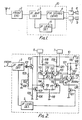
- the FM carrier wave including the (L+R) signal, the AM suppressed carrier of 38 kHz modulated by the (L-R) signal, and the pilot signal of 19 kHz etc. is received at an antenna 1, and supplied to the circuit 2 (usually called the "front end").
- This circuit 2 comprises a radio frequency amplifier (RF Amp.), the local oscillator (osc), and mixer, and supplies the intermediate frequency (IF).
- RF Amp. radio frequency amplifier
- osc local oscillator
- IF intermediate frequency
- the output signal is supplied to the next IF Amp" and to the FM detector 3, to obtain the composite signal.
- This composite signal is supplied to the FM stereo signal demodulator 4, while part of the output from the IF amp.
- This IF level detector 5 supplies a DC voltage, in accordance with the IF signal, to the FM stereo signal demodulator 4. This output from the IF level detector 5 is used to control the separation of the demodulator 5. Thus when the electric field strength of the received signal is high this output is supplied to the demodulator 5 to make the separation great, and when the strength is low the output is supplied to make the separation small.
- the separated left and right signals are supplied to the Audio Frequency Amplfiers (AF Amp.) 6 and 7 and thence to the loudspeakers 8 and 9.
- AF Amp. Audio Frequency Amplfiers
- Figure 2 shows a preferred embodiment of the part of Figure 1 enclosed by dotted lines.
- the composite signal from the detector 3 is supplied via capacitor 101 to the base of transistor 102 operating as an emitter follower.
- the emitter of transistor 102 is grounded through resistance 105, and its collector is connected to power supply terminal 130.
- the signal appearing at the emitter of transistor 102 is supplied to the base of a first input transistor 114.
- a DC bias source 128 is connected to the base of transistor 102 and to a second emitter follower 107 through resistances 103 and 104 respectively. As the junction of the resistances 103 and 104 is ground to any alternating signal, the composite signal is not supplied to the base of transistor 115.
- the emitter of transistor 107 is grounded through resistance 106, and its collector is connected to the power supply terminal 130.
- the collector of the first input transistor 114 is connected to the junction of the emitters of a pair of transistors 110 and 111 which are operated as a first synchronous demodulator 20.
- the collectors of these transistors are connected to the power supply terminal 13Q through resistances 108 and 109 respectively.
- the emitter of transistor 114 is connected to the emitter of the second input transistor 115 through the resistances 116 and 117, and the junction of resistances 116 and is grounded through resistance 118,
- the collector of the second input transistor 115 is connected to the emitters of a pair of transistors 112 and 113 which are operated as a second synchronous demodulator 30, the collectors of these transistors being connected to the collectors of transistors 110 and 111 respectively. In this way the outputs of said first synchronous demodulator 20 and said second synchronous demodulator 30 are added.
- the left and right signals which appear at the output terminals 119 and 120 are supplied to the AF amplifiers 6 and 7.
- An output from the IF level detector 5 is supplied to the base of a third input transistor 127.
- the IF level detector 5 detects the output of the IF Amp. 3, and rectifies the output to a DC voltage before applying it to transistor 127.
- the output drive a Signal Strength Meter.
- the emitter of the third input transistor 127 is grounded, and its collector is connected to the junction of the emitters of a pair of transistors 123 and 124 operating as a gate circuit 40.
- the collectors of these transistors 123 and 124 are connected to the DC voltage source 129 through resistances 121 and 122 respectively.
- the 38 kHz switching signals is applied to the bases of these transistors 123 and 124, via terminals 125 and 126.
- This 38 kHz signal is, for example, obtained from the 19 kHz pilot signal to be doubled by a frequency doubler (not shown).
- the collector of transistor 123 is connected to the bases of transistors 110 and 113, and the collector of transistor 124 is connected to the bases of the transistors 111 and 112.
- pairs of transistors 110 and 113, 111 and 112 are kept in the same conductive condition. That is to say, when transistors 111 and 112 are conductive, transistors 110 and 113 are nonconductive and vice versa at the next half cycle of the 38 kHz switching signal.
- a synchronous demodulator of the type used as the demodulator 20 produces a substantially equal and predictable amount of undesirable crosstalk at each of the output terminals 119 and 120.
- the composite signal applied to the second sycnhronous demodulator 30 is supplied through the resistances 116, 117 to the emitter of the second input transistor 115 from the emitter of the first input transistor 114.
- the composite signal to be supplied to the second demodulator 30 is out of phase with the composite signal supplied to the first synchronous demodulator 20, and so if the ratio of the composite signal at the collector of transistor 114 to that at the collector of transistor 115 is 1:1/k, the output of the second synchronous demodulator 30 can be expressed as: wherein L 2 and R 2 are signals which appear at the collectors of transistors 112 and 113 respectively.
- the ratio of the collector current of the transistor 110 to111, or 113 to 112 can be as follows : or wherein I c110 ,I c111 , Icll2 and I c113 are the collector current of transistors 110, 111, 112 and 113 respectively "a" having a value in the range 0.5 ⁇ a ⁇ 1.
- the voltage difference between the collectors of transistors 123 and 124 is wherein q: the charge of an electron, k: Boltzman's constant, T: absolute temperature, I 1 : collector currents of transistors 110, 113, I 2 : collector current of transistors 111, 112. when therefore from equations (20) and (18) and also the separation S is, from the equations (13) and (21)
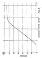
- This equation (22) shows the the separation S varies 10 proportion to the V BB38
- This relationship is shown in Figure which shows the relationship becween the separation of the FM stereo signal demodulator and the separation control voltage supplied to the base of the transistor 123.
- V BB38 is varied by varying the voltage drop of the resistances 121 and 122 by controlling the separation control voltage.
Landscapes
- Engineering & Computer Science (AREA)
- Power Engineering (AREA)
- Signal Processing (AREA)
- Stereo-Broadcasting Methods (AREA)
Applications Claiming Priority (2)
| Application Number | Priority Date | Filing Date | Title |
|---|---|---|---|
| JP160435/78 | 1978-12-25 | ||
| JP16043578A JPS5586235A (en) | 1978-12-25 | 1978-12-25 | Fm stereo signal demodulator |
Publications (2)
| Publication Number | Publication Date |
|---|---|
| EP0013149A1 true EP0013149A1 (de) | 1980-07-09 |
| EP0013149B1 EP0013149B1 (de) | 1983-04-06 |
Family
ID=15714862
Family Applications (1)
| Application Number | Title | Priority Date | Filing Date |
|---|---|---|---|
| EP79302992A Expired EP0013149B1 (de) | 1978-12-25 | 1979-12-20 | FM Stereosignal-Demodulator |
Country Status (4)
| Country | Link |
|---|---|
| US (1) | US4466115A (de) |
| EP (1) | EP0013149B1 (de) |
| JP (1) | JPS5586235A (de) |
| DE (1) | DE2965165D1 (de) |
Families Citing this family (6)
| Publication number | Priority date | Publication date | Assignee | Title |
|---|---|---|---|---|
| JPS57208743A (en) * | 1981-06-17 | 1982-12-21 | Pioneer Electronic Corp | Stereo demodulation circuit |
| US4607381A (en) * | 1984-10-05 | 1986-08-19 | Sony Corporation | Signal mixing circuit |
| JPH0669150B2 (ja) * | 1985-05-16 | 1994-08-31 | クラリオン株式会社 | Fm受信機 |
| US4646348A (en) * | 1985-07-18 | 1987-02-24 | National Semiconductor Corporation | Blend control for low voltage stereo decoders |
| US5027402A (en) * | 1989-12-22 | 1991-06-25 | Allegro Microsystems, Inc. | Blend-on-noise stereo decoder |
| DE4235909C2 (de) * | 1992-10-23 | 2003-01-02 | Atmel Germany Gmbh | Mono/Stereo-Umschalter |
Citations (6)
| Publication number | Priority date | Publication date | Assignee | Title |
|---|---|---|---|---|
| US3634626A (en) * | 1970-04-06 | 1972-01-11 | Sylvania Electric Prod | Noise-operated automatic stereo to monaural switch for fm receivers |
| US3790714A (en) * | 1970-07-13 | 1974-02-05 | Sony Corp | Fm stereophonic receiver |
| US3798376A (en) * | 1969-12-29 | 1974-03-19 | Rca Corp | Multiplex decoding system |
| DE2461134A1 (de) * | 1973-12-27 | 1975-07-10 | Rediffusion Ag | Stereophonie-empfaenger |
| DE2534310A1 (de) * | 1974-08-01 | 1976-02-19 | Nippon Musical Instruments Mfg | Rauschunterdrueckungsvorrichtung fuer einen fm-stereoempfaenger |
| US4032717A (en) * | 1975-03-13 | 1977-06-28 | Siemens Aktiengesellschaft | Circuit arrangement for a continuous adjustment of the base width in a stereo decoder |
Family Cites Families (6)
| Publication number | Priority date | Publication date | Assignee | Title |
|---|---|---|---|---|
| DE2004572A1 (de) * | 1969-02-07 | 1971-03-04 | Motorola Inc | Multiplex Demodulatorschaltung fur einen Stereo Empfanger |
| US3752934A (en) * | 1969-12-19 | 1973-08-14 | N Shoichi | Stereo demodulating circuit triggered by a minimum input signal level |
| US3711652A (en) * | 1971-03-10 | 1973-01-16 | Gen Electric | Monolithic stereo decoder with balanced decoder operation |
| US3825697A (en) * | 1973-07-27 | 1974-07-23 | Gen Motors Corp | Phase-lock-loop fm-stereo decoder including stereophonic/monophonic blend system for reducing audio distortion |
| JPS5243303A (en) * | 1975-10-01 | 1977-04-05 | Pioneer Electronic Corp | Reversion circuit of fm stereo |
| JPS5828776B2 (ja) * | 1977-05-17 | 1983-06-17 | 株式会社ケンウッド | 出力制御回路 |
-
1978
- 1978-12-25 JP JP16043578A patent/JPS5586235A/ja active Pending
-
1979
- 1979-11-19 US US06/095,385 patent/US4466115A/en not_active Expired - Lifetime
- 1979-12-20 EP EP79302992A patent/EP0013149B1/de not_active Expired
- 1979-12-20 DE DE7979302992T patent/DE2965165D1/de not_active Expired
Patent Citations (6)
| Publication number | Priority date | Publication date | Assignee | Title |
|---|---|---|---|---|
| US3798376A (en) * | 1969-12-29 | 1974-03-19 | Rca Corp | Multiplex decoding system |
| US3634626A (en) * | 1970-04-06 | 1972-01-11 | Sylvania Electric Prod | Noise-operated automatic stereo to monaural switch for fm receivers |
| US3790714A (en) * | 1970-07-13 | 1974-02-05 | Sony Corp | Fm stereophonic receiver |
| DE2461134A1 (de) * | 1973-12-27 | 1975-07-10 | Rediffusion Ag | Stereophonie-empfaenger |
| DE2534310A1 (de) * | 1974-08-01 | 1976-02-19 | Nippon Musical Instruments Mfg | Rauschunterdrueckungsvorrichtung fuer einen fm-stereoempfaenger |
| US4032717A (en) * | 1975-03-13 | 1977-06-28 | Siemens Aktiengesellschaft | Circuit arrangement for a continuous adjustment of the base width in a stereo decoder |
Non-Patent Citations (1)
| Title |
|---|
| FUNKSCHAU, Vol. 47, No. 10, 1975 Munchen D. MALLON "Monolithischer PLL-Stereo-Decoder" pages 193 to 196 * Page 194; fig. 3 * * |
Also Published As
| Publication number | Publication date |
|---|---|
| DE2965165D1 (en) | 1983-05-11 |
| EP0013149B1 (de) | 1983-04-06 |
| JPS5586235A (en) | 1980-06-28 |
| US4466115A (en) | 1984-08-14 |
Similar Documents
| Publication | Publication Date | Title |
|---|---|---|
| EP0331234B1 (de) | Schaltungsanordnung zum linearen Verstärken und Demodulieren eines AM-modulierten Signals und dazu geeignetes integriertes Halbleiterelement | |
| US4380824A (en) | Receiving reproducing system | |
| US4907293A (en) | Adjacent channel interference suppressing system for FM receiver | |
| EP0018608A2 (de) | Störunterdrückungsschaltung | |
| US4356350A (en) | FM Receiver | |
| US4063039A (en) | Stereo noise reduction circuit | |
| US3825697A (en) | Phase-lock-loop fm-stereo decoder including stereophonic/monophonic blend system for reducing audio distortion | |
| US4140878A (en) | Stereo demodulator system | |
| US4074075A (en) | Circuit for demodulating a stereo signal | |
| EP0013149B1 (de) | FM Stereosignal-Demodulator | |
| US4399325A (en) | Demodulating circuit for controlling stereo separation | |
| US4146747A (en) | Fm stereo demodulating device | |
| US4512031A (en) | Arrangement for receiving TV-signals having left and right stereo sound signals | |
| US4047116A (en) | FM multiplex stereo demodulating circuit | |
| US4349696A (en) | AM Stereophonic demodulator circuit for amplitude/angle modulation system | |
| EP0448144A2 (de) | Signalverarbeitungsschaltung | |
| US4607381A (en) | Signal mixing circuit | |
| EP0056270A1 (de) | Tonsignaldemodulatorgerät für einen Fernsehempfänger | |
| EP0047522B1 (de) | Schaltungsanordnung zur Identifizierung eines Stereo-Signals | |
| JPS6239858B2 (de) | ||
| US4710958A (en) | Circuit for controlling separation and high-cut operation of a stereo demodulator in an FM radio receiver | |
| US3339025A (en) | De-emphasis network arrangement for am-fm radios | |
| GB2040145A (en) | Improvements in F.M. receivers | |
| US3526720A (en) | Stereo attachment for standard frequency modulation receiver | |
| US3339024A (en) | Time sampling stereophonic receiver circuit |
Legal Events
| Date | Code | Title | Description |
|---|---|---|---|
| PUAI | Public reference made under article 153(3) epc to a published international application that has entered the european phase |
Free format text: ORIGINAL CODE: 0009012 |
|
| AK | Designated contracting states |
Designated state(s): DE FR GB NL |
|
| 17P | Request for examination filed | ||
| GRAA | (expected) grant |
Free format text: ORIGINAL CODE: 0009210 |
|
| AK | Designated contracting states |
Designated state(s): DE FR GB NL |
|
| ET | Fr: translation filed | ||
| REF | Corresponds to: |
Ref document number: 2965165 Country of ref document: DE Date of ref document: 19830511 |
|
| PLBI | Opposition filed |
Free format text: ORIGINAL CODE: 0009260 |
|
| PLBI | Opposition filed |
Free format text: ORIGINAL CODE: 0009260 |
|
| 26 | Opposition filed |
Opponent name: GRUNDIG E.M.V. ELEKTRO-MECHANISCHE VERSUCHSANSTALT Effective date: 19831221 |
|
| 26 | Opposition filed |
Opponent name: INTERESSENGEMEINSCHAFT FUER RUNDFUNKSCHUTZRECHTE G Effective date: 19840105 |
|
| RAP2 | Party data changed (patent owner data changed or rights of a patent transferred) |
Owner name: KABUSHIKI KAISHA TOSHIBA |
|
| PLAB | Opposition data, opponent's data or that of the opponent's representative modified |
Free format text: ORIGINAL CODE: 0009299OPPO |
|
| REG | Reference to a national code |
Ref country code: FR Ref legal event code: CD |
|
| R26 | Opposition filed (corrected) |
Opponent name: GRUNDIG E.M.V. ELEKTRO-MECHANISCHE VERSUCHSANSTALT Effective date: 19831221 |
|
| REG | Reference to a national code |
Ref country code: GB Ref legal event code: 746 |
|
| PLAB | Opposition data, opponent's data or that of the opponent's representative modified |
Free format text: ORIGINAL CODE: 0009299OPPO |
|
| R26 | Opposition filed (corrected) |
Opponent name: GRUNDIG E.M.V. ELEKTRO-MECHANISCHE VERSUCHSANSTALT Effective date: 19831221 |
|
| PLAB | Opposition data, opponent's data or that of the opponent's representative modified |
Free format text: ORIGINAL CODE: 0009299OPPO |
|
| R26 | Opposition filed (corrected) |
Opponent name: GRUNDIG E.M.V. ELEKTRO-MECHANISCHE VERSUCHSANSTALT Effective date: 19831221 |
|
| PLBN | Opposition rejected |
Free format text: ORIGINAL CODE: 0009273 |
|
| STAA | Information on the status of an ep patent application or granted ep patent |
Free format text: STATUS: OPPOSITION REJECTED |
|
| 27O | Opposition rejected |
Effective date: 19881213 |
|
| NLR2 | Nl: decision of opposition | ||
| PGFP | Annual fee paid to national office [announced via postgrant information from national office to epo] |
Ref country code: FR Payment date: 19981209 Year of fee payment: 20 |
|
| PGFP | Annual fee paid to national office [announced via postgrant information from national office to epo] |
Ref country code: GB Payment date: 19981224 Year of fee payment: 20 |
|
| PGFP | Annual fee paid to national office [announced via postgrant information from national office to epo] |
Ref country code: NL Payment date: 19981229 Year of fee payment: 20 Ref country code: DE Payment date: 19981229 Year of fee payment: 20 |
|
| PG25 | Lapsed in a contracting state [announced via postgrant information from national office to epo] |
Ref country code: GB Free format text: LAPSE BECAUSE OF EXPIRATION OF PROTECTION Effective date: 19991219 |
|
| PG25 | Lapsed in a contracting state [announced via postgrant information from national office to epo] |
Ref country code: NL Free format text: LAPSE BECAUSE OF EXPIRATION OF PROTECTION Effective date: 19991220 |
|
| REG | Reference to a national code |
Ref country code: GB Ref legal event code: PE20 Effective date: 19991219 |
|
| NLV7 | Nl: ceased due to reaching the maximum lifetime of a patent |
Effective date: 19991220 |
|
| APAH | Appeal reference modified |
Free format text: ORIGINAL CODE: EPIDOSCREFNO |