EP0014310A1 - Dispositif pour la polarisation d'un substrat - Google Patents
Dispositif pour la polarisation d'un substrat Download PDFInfo
- Publication number
- EP0014310A1 EP0014310A1 EP80100036A EP80100036A EP0014310A1 EP 0014310 A1 EP0014310 A1 EP 0014310A1 EP 80100036 A EP80100036 A EP 80100036A EP 80100036 A EP80100036 A EP 80100036A EP 0014310 A1 EP0014310 A1 EP 0014310A1
- Authority
- EP
- European Patent Office
- Prior art keywords
- electrode
- mosfet
- substrate
- semiconductor substrate
- capacitor
- Prior art date
- Legal status (The legal status is an assumption and is not a legal conclusion. Google has not performed a legal analysis and makes no representation as to the accuracy of the status listed.)
- Granted
Links
Images


Classifications
-
- H—ELECTRICITY
- H10—SEMICONDUCTOR DEVICES; ELECTRIC SOLID-STATE DEVICES NOT OTHERWISE PROVIDED FOR
- H10D—INORGANIC ELECTRIC SEMICONDUCTOR DEVICES
- H10D89/00—Aspects of integrated devices not covered by groups H10D84/00 - H10D88/00
- H10D89/211—Design considerations for internal polarisation
- H10D89/213—Design considerations for internal polarisation in field-effect devices
- H10D89/215—Design considerations for internal polarisation in field-effect devices comprising arrangements for charge pumping or biasing substrates
-
- G—PHYSICS
- G05—CONTROLLING; REGULATING
- G05F—SYSTEMS FOR REGULATING ELECTRIC OR MAGNETIC VARIABLES
- G05F3/00—Non-retroactive systems for regulating electric variables by using an uncontrolled element, or an uncontrolled combination of elements, such element or such combination having self-regulating properties
- G05F3/02—Regulating voltage or current
- G05F3/08—Regulating voltage or current wherein the variable is DC
- G05F3/10—Regulating voltage or current wherein the variable is DC using uncontrolled devices with non-linear characteristics
- G05F3/16—Regulating voltage or current wherein the variable is DC using uncontrolled devices with non-linear characteristics being semiconductor devices
- G05F3/20—Regulating voltage or current wherein the variable is DC using uncontrolled devices with non-linear characteristics being semiconductor devices using diode- transistor combinations
- G05F3/205—Substrate bias-voltage generators
-
- H—ELECTRICITY
- H10—SEMICONDUCTOR DEVICES; ELECTRIC SOLID-STATE DEVICES NOT OTHERWISE PROVIDED FOR
- H10D—INORGANIC ELECTRIC SEMICONDUCTOR DEVICES
- H10D88/00—Three-dimensional [3D] integrated devices
Definitions
- the invention relates to a substrate bias generator for producing a potential in a semiconductor substrate, and more particularly to such a generator used with a dynamic memory cell in the form of an integrated circuit including, as the fundamental element, at least one MOS field effect transistor (abbreviated hereinafter as "MOSFET").
- MOSFET MOS field effect transistor
- Conventional substrate bias generators comprised a MOS capacitor and one pair of serially connected MOSFET's with the gate electrode connected to the drain electrode disposed on one of opposite main faces of the P type semiconductor substrate and interconnected so that the MOS capacitor is connected to the junction of the MOSFET, and one of the MOSFET's includes a source electrode normally put at a ground potential while the other MOSFET hat the drain electrode connected to an electrode on the other main face of the substrate. Therefore, a parasitic diode is formed between a pair of N type semiconductor regions forming an electrode for the MOS capacitor and a combined drain and source region of both MOSFET's, respectively, and the substrate, while these regions and the substrate are attended with parasitic capacitances to ground.
- the dynamic memory cell includes a single MOSFET and a single MOS capacitor serially connected to each other, and stores data expressed by a binary ONE by having the MOS capacitor charged to a high potential.
- the MOS capacitor changes from the high potential to a low potential which may reach a ground potential corresponding to a binary ZERO as the case may be. This has resulted in malfunction of the dynamic memory cell that a binary ZERO is read out although the binary ONE ought to have been written in the cell.
- the invention as claimed is intended to provide a remedy by providing an improved substrate bias generator for producing a potential in a semiconductor substrate disposed in an integrated circuit on a semiconductor chip to permit a very small number of electrons to be injected into an associated semiconductor substrate to remove the principal factor for malfunction in a dynamic memory cell in the form of an integrated circuit disposed on the same chip as the generator.
- a substrate bias generator for generating a potential in a semiconductor substrate, comprising a semiconductor substrate of a first type conductivity and including a pair of first and second main faces opposite to each other, a first, a second and a third semiconductor region of a second type conductivity disposed in predetermined intervals on the first main face of the semiconductor substrate, a first MOSFET disposed on the first main face of the semiconductor substrate and including a source region formed on the first semiconductor region, a drain region formed of said second semiconductor region and a gate electrode, a second MOSFET disposed on the first main face of the semiconductor substrate and including a source region formed of the second semiconductor region, a drain region formed of the third semiconductor region, and a gate electrode, a capacitor disposed on the first main face of the semiconductor substrate through an electrically insulating film, the capacitor including a pair of opposite electrodes and another electrically insulating film interposed between the electrodes, a first electrical lead for connecting one of the electrodes of the capacitor to the gate electrode and drain region
- the capacitor may include one electrode disposed on the first main face of the semiconductor substrate through the electrically insulating film and connected to the gate electrode and the drain region of the first MOSFET through the first electric lead and the other electrode disposed on the one electrode through the abovementioned another electrically insulating film and applied with the signal.
- Figure 1 shows a conventional substrate bias generator for producing a potential in a semiconductor substrate.
- the arrangement illustrated comprises a P type semiconductor substrate 10 having a high resistivity and including a pair of first and second main faces opposite to each other, and a plurality of N + type low resistivity semiconductor regions, in this case, five regions 12, 14, 16 and 18 disposed in predetermined intervals on the first main face, in this case, the upper main face of the substrate 10.
- the two N + type semiconductor regions 12 are interconnected through an N type semiconductor layer 20 disposed on the upper main face of the substrate to act as an electrode for a MOS type capacitor 22 including a thin electrically insulating film 24 underlaid with the N type semiconductor layer 20 and adjacent portions of the semiconductor regions 12 and a region 26 disposed on the electrically insulating film 24.
- the electrically insulating film 24 is, in many cases, formed of silicon dioxide and is called hereinafter a "gate oxide film", while the region 26 is formed of polycrystalline silicon, aluminum or molybdenum.
- the N type semiconductor regions 14 and 16 form respectively a source and a drain region of a first M O S -FET 28 including a gate oxide film 30 similar to the gate oxide film 24 and disposed on the upper main face of the substrate 10 so as to bridge the regions 14 and 16, and a region 32 formed on the gate oxide film 30 of polycrystalline silicon or the like.
- the gate oxide film 30 and the region 32 form a part of the gate region of the MOSFET 28.
- the N + type semiconductor region 16 also forms a source region of a second MOSFET 34 including a gate oxide film 36 similar to the gate oxide film 30 and a region 38 similar to the region 32, while the N + type semiconductor region 18 forms the drain region of the MOSFET 34.
- the gate oxide film 36 similarly forms a part of the gate region of the MOSFET 34 with the region 38.
- an electrode 4C is connected to the region 26 forming the other electrode of the MOS capacitor 22, and electrodes 43 are connected to the N + type semiconductor regions 12, respectively, and to each other.
- a source, a gate and a drain electrode 44, 46 and 48 are connected to the source region 14, the region 32 and the drain regions of the first MOSFET 28, respectively.
- a gate and a drain electrode 52 are connected to the region 38 and the drain region 18 of the second MOSFET 34.
- an electrode 54 is connected to the second or lower main face of the semiconductor substrate 10.
- the electrodes 42, the gate electrode 32 and the drain electrode 48 are connected to one another through a first electric lead 56, while the gate electrode 50, the drain electrode 52 and the electrode 54 are connected to one another through a second electric lead 58.
- Figure 2 shows a circuit equivalent to the arrangement of Figure 1.
- like reference numerals designate the components identical to those shown in Figure 1.
- a parasitic diode 60 is shown as being formed between the N type semiconductor regions 12 and the P type semiconductor substrate 10 due to a PN junction formed therebetween
- a parasitic diode 62 is shown as being formed between the N + type semiconductor region 16 and the P type semiconductor substrate 10 due to a PN junction formed therebetween.
- Further parasitic capacitances 64 and 66 to ground are produced on the N type semiconductor regions 12, 16 and the semiconductor substrate 10, respectively.
- signals are generally transmitted therethrough by charging and discharging the source electrode and/or the drain electrode of MOSFET's, and the higher the charging and discharging rates, the more the operation of the integrated circuits is speeded up. For example, random access memory devices are required to shorten the access time.
- One of the important factors for determining the charging and discharging rates is a junction capacitance of a PN junction relative to the particular semiconductor substrate appearing on either of the source and drain regions of each MOSFET involved. The smaller this junction capacitance, the less the charging and discharging rates will be.
- the junction capacitance C may be generally expressed by where V designates a built-in potential at the P N junction which is normally of about 0,6 volts, V a voltage across either of the source and drain regions of the MOSFET and the semiconductor substrate and holds V ⁇ O, and K designates a constant as determined by the type of a semiconductive material involved and the dimension of the MOSFET. Since V and K are constants o as determined by the type of the semiconductive material and the dimension of the MOSFET's, the junction capacitance C J is permitted to decrease only with a small degree of freedom. This means that the junction capacitance C J can decrease only by increasing the voltage V in a negative sense.
- MOSFET's have the source (or drain) voltage the magnitude of which generally ranges from ground potential to a voltage across an electric source used with the particular integrated circuit, for example, +5 volts.
- a potential difference V between the source (or drain) voltage and a voltage applied to the semiconductor substrate has a magnitude between the ground potential and -5 volts.
- a voltage of, for example, -3 volts applied to the semiconductor substrate that potential difference V has a magnitude of from -3 to -8 volts.
- equation (1) indicates that the junction capacitance C J becomes small resulting in the attainment of high speed operation.
- an external electric (power) source has been previously used to apply a potential to an associated semiconductor substrate through an electrode such as the electrode 54 shown in Figure 1.
- the arrangement of Figure 2 produces'a negative voltage on an associated integrated circuit formed of MOSFET's to supply it to the electrode 54 in order to eliminate waste when the external electric source is prepared.
- the electrode 40 shown in Figure 2 is fed with an output signal delivered from an oscillator such as a ring oscillator, a trigger circuit or the like disposed on an integrated circuit.
- the output signal may be of square waveform as shown in Figure 3.
- this output signal is shown as forming a source voltage V DD supplied to the arrangement shown in Figure 1 as being constructed into an integrated circuit.
- V DD source voltage supplied to the arrangement shown in Figure 1 as being constructed into an integrated circuit.
- this MOSFET is brought into its conducting state with the potential on the electric lead 56 equal to about the threshold voltage V T (28) of the MOSFET 28.
- the potential on the electric lead 56 has its magnitude varying between V (28) and -(Vp - V T (28) ) ⁇ -(V DD - V T (28)), as shown at square waveform b in Figure 3.
- V (28) and -(Vp - V T (28) ) ⁇ -(V DD - V T (28)) the potential on the electric lead 56 has its magnitude varying between V (28) and -(Vp - V T (28) ) ⁇ -(V DD - V T (28)), as shown at square waveform b in Figure 3.
- the substrate potential has a magnitude selectively expressed by and dependent upon the relative magnitudes of V T (34), V F (60) and V F (62), where V T (32) designates the threshold voltage of the MOSFET 34 and V F (60) and F F (62) designate forward voltage drops across the diodes 60 and 62, respectively.
- the solid curve depicts the current component of the discharging current discharged through the diodes 60 and 62, while the dotted curve depicts that current component thereof discharged through the MOSFET 34.
- V T (34) > V F (60) VF(62) holds, the substrate potential is discharged to -(V DD - V T (28) - V (60) in the steady state. As a result the substrate potential has the ultimate magnitude as shown at waveform C or the lowermost solid line in Figure 4.
- V T (34) ⁇ V F (60) V F (62) holds, the discharging current from the capacitor 66 includes a current component through the diodes 60 and 62 smaller than that through the MOSFET 34. Therefore, the substrate potential has the ultimate magnitude expressed by -( V DD - V T (28) - VT(32)) in the steady state.
- the substrate bias generator as shown in Figure 1 performs such an operation that electrons are injected into the P type semiconductor substrate through the parasitic diodes 60 and 62, on the one hand, and the electrons passing through the MOSFET 34 reach the electrode 54 connected to the second or lower main face of the substrate, on the other hand. Therefore the shortage of holes is established in the substrate resulting in the substrate potential reaching a negative magnitude. More specifically, the electrons injected into the substrate through the diodes 60 and 62 live within the substrate for a short time interval after which they disappear through their recombination with holes which form majority carriers in P type semiconductive materials.
- the arrangement illustrated comprises a P type semiconductor substrate 110 having a high resistivity and including a pair of opposite main faces, and a pair of type low resistivity semiconductor regions 112 and 114 disposed on one of the main faces, in this case, the upper main face as viewed in Figure 5 of the substrate 110, to form a predetermined spacing therebetween.
- the N type semiconductor regions 112 and 114 act as a drain and a source region of a MOSFET 116 including a gate oxide film 118 underlaid with that portion of the upper main face of the substrate 110 defined by the semiconductor regions 112 and 114 and the adjacent portions of the latter, and a gate electrode 120 disposed on the gate oxide film 118.
- the drain region 112 is connected to an electric lead 122 which is called a "bit line”
- the gate electrode 120 is connected to an electric lead 124 called a "word line”.
- anbther gate oxide film 118' overlaid with another gate electrode 120' is disposed on the upper main face of the substrate 110 so that one end thereof is located on the end portion of the semiconductor region 114 remote from the gate oxide film 118, and the other end thereof is spaced from the region 114 by a predetermined distance.
- the gate oxide film 118' and gate electrode 120' form parts of an MOS type capacitor 116', as will be described later.
- the gate electrode 120' is connected to an electric lead 124' having normally applied thereto a maximum voltage, for example of +5 volts, used with the arrangement of Figure 5.
- the MOS type capacitor 106' is formed between the source region 114 and the gate electrode 120'.
- an electrode 126 is connected to the other or lower main face of the substrate 110.
- Figure 5 forms an equivalent circuit as shown in Figure 6 wherein like reference numerals designate the components identical to those illustrated in Figure 5.
- the bit line 122 is put at a high potential.
- the word line 124 is put a a high potential to bring the MOSFET 116 into its conducting state.
- This conduction of the MOSFET 116 causes the potential in the bit line 122 to be transferred to the source region 114 of the MOSFET 116. Therefore, the MOS type capacitor 116' is charged to the high potential. At that time, the number of electrons becomes very small within the MOS capacitor 116'.
- the word line 124 is returned back to a low potential, whereupon the MOSFET 116 is put in its nonconducting,state. Accordingly, the bit line 122 is electrically isolated from the source region 114 with the result that the MOS type capacitor 116' charged to the high potential is left intact. At that time, the memory cell stores and holds written data corresponding to the binary ONE.
- the substrate bias generator shown in Figures 1 and 2 is operated to inject electrons into the substrate 10 through the diodes 60 and 62.
- some of the electrons thus injected may reach the vicinity of the MOS type capacitor 116' as shown at the arrow 128 in Figure 5.
- the electrons form minority carriers within the P type semiconductor substrate 110, the electrons are normally recombined with holes and disappear, while the electrons are not so spaced from a source into which they have been injected. According to circumstances, however, some of the injected electrons reach the vicinity of the memory cell.
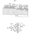
- FIG 7 there is illustrated one embodiment of a substrate bias generator for generating a potential in a semiconductor substrate according to the present invention.
- the arrangement illustrated is different from that shown in Figure 1 only in that in Figure 7 a parallel plate type capacitor is substituted for the MOS type capacitor shown in Figure 1. Therefore, like reference numerals of the 200 series have been employed to identify the components identical or corresponding to those shown in Figure 1, and the description will now be directed only to the difference between the arrangements shown in Figures 1 and 7, respectively.
- the MOS type capacitor 20 shown in Figure 1 is omitted and instead a silicon dioxide film 270 is disposed on the upper main face of the P type semiconductor substrate 210 to extend substantially between positions occupied by the outer sides of the opposite N type semiconductor regions 12 which have been now omitted with the N type semiconductor layer 20 sandwiched therebetween.
- the silicon dioxide film 270 is substituted for the gate oxide film 24 shown in Figure 1, but thicker than the gate oxide films 230 and 236 included in the MOSFET's 228 and 324, respectively.
- a first region 272 is formed on the gate oxide film 270 of polycrystalline silicon to form a first layer.
- the region 272 is preferably formed by the well known irradiation with light or an electron beam simultaneously with the regions 232 and 252 included in the MOSFET's 228 and 234, respectively.
- a silicon dioxide film 224 is disposed on the first layer 272 to cause the bilateral end portions as viewed in Figure 7 of the first layer 270 to be exposed for the purpose as will be apparent subsequently.
- the silicon dioxide film 224 is overlaid with a second layer 226 formed of polycrystalline silicon, and the electrode 240 is connected to the second layer 226, while the electrodes 242 are connected to the exposed portions of the first layer 272 and to each other.
- the electrodes 240 and 242 have a parallel plate capacitor 222 formed therebetween and including an electrically insulating film composed of the silicon dioxide film 224.
- the electrode 272 is connected to the electrodes 246 and 248 for the MOSFET 228 through the lead 256 as in the arrangement shown in Figure 1.
- Figure 7 forms an equivalent circuit as shown in Figure 8, wherein like reference numerals designate the components identical to those illustrated in Figure 7.
- the equivalent circuit illustrated is different from that shown in Figure 2 only in that in Figure 8 a single parasitic diode 262 is formed between the N type semiconductor region 216 and the P type semiconductor substrate 210, in addition to the substitution of the parallel plate type capacitor 222 for the MOS type capacitor 22.
- Figures 7 and 8 The arrangement shown in Figures 7 and 8 is fundamentally identical in operation to that described above in conjunction with. Figures 1 through 4 in view of the fact that the substrate bias generator is integrated with the dynamic memory cell in a common semiconductor chip.
- an electron-stream is injected into the substrate 210 through the MOSFET 234 and the lower or second main face of the substrate 210 until electrons included in the latter stream are immediately recombined with holes in the vicinity of the second main face and disappear resulting in a hole stream.
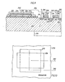
- the second layer 236 has an inverted U-shaped cross-section so as to bridge in intimate contact relationship the first layer 272 through the silicon dioxide film 224.
- the second layer 272 has folded ends of both legs of the "U” fixedly secured to the gate oxide film 270 and causes the exposure of the opposite end portions of the first layer 272 extending in the direction of width of the legs of the "U” (see Figure 10).
- the electrodes 240 are connected to the exposed end portions of the first layer 272 and to each other, while the electrode 242 is connected to the central portion of the second layer 226, as shown in Figure 10.
- the electrode 240 corresponds to the electrode 40 shown in Figures 1 and 2, and electrode 242 is connected to the junction of the MOSFET's 228 and 234.
- a coupling capacitor is formed of two layers of polycrystalline silicon serving as electrodes and a thin silicon dioxide film sandwiched therebetween and underlaid with a thick silicon dioxide film disposed on a first main face of a semiconductor chip, thereby to be electrically insulated from the semiconductor substrate.
- the coupling capacitor forms a part of the substrate bias generator integrated with a dynamic memory cell disposed on the same chip as the generator.
- PN junction formed between a P type semiconductor substrate included in that chip and an associated N + type semiconductor region is small in area as compared with the prior art practice, resulting in an extremely small risk for malfunction of the dynamic memory cell.
Landscapes
- Engineering & Computer Science (AREA)
- Physics & Mathematics (AREA)
- Microelectronics & Electronic Packaging (AREA)
- Nonlinear Science (AREA)
- Electromagnetism (AREA)
- General Physics & Mathematics (AREA)
- Radar, Positioning & Navigation (AREA)
- Automation & Control Theory (AREA)
- Semiconductor Integrated Circuits (AREA)
- Metal-Oxide And Bipolar Metal-Oxide Semiconductor Integrated Circuits (AREA)
- Semiconductor Memories (AREA)
Applications Claiming Priority (2)
| Application Number | Priority Date | Filing Date | Title |
|---|---|---|---|
| JP88379A JPS5593252A (en) | 1979-01-05 | 1979-01-05 | Substrate potential generating apparatus |
| JP883/79 | 1979-01-05 |
Publications (2)
| Publication Number | Publication Date |
|---|---|
| EP0014310A1 true EP0014310A1 (fr) | 1980-08-20 |
| EP0014310B1 EP0014310B1 (fr) | 1982-12-29 |
Family
ID=11486061
Family Applications (1)
| Application Number | Title | Priority Date | Filing Date |
|---|---|---|---|
| EP80100036A Expired EP0014310B1 (fr) | 1979-01-05 | 1980-01-04 | Dispositif pour la polarisation d'un substrat |
Country Status (4)
| Country | Link |
|---|---|
| US (1) | US4255756A (fr) |
| EP (1) | EP0014310B1 (fr) |
| JP (1) | JPS5593252A (fr) |
| DE (1) | DE3061453D1 (fr) |
Cited By (6)
| Publication number | Priority date | Publication date | Assignee | Title |
|---|---|---|---|---|
| EP0048474A1 (fr) * | 1980-09-24 | 1982-03-31 | Kabushiki Kaisha Toshiba | Dispositif pour polarisation automatique de substrat |
| EP0084177A3 (en) * | 1982-01-14 | 1985-04-10 | Kabushiki Kaisha Toshiba | A semiconductor device having a back-gate bias generator |
| EP0165766A1 (fr) * | 1984-06-20 | 1985-12-27 | American Microsystems, Incorporated | Circuit filtre intégré |
| US4853759A (en) * | 1986-09-29 | 1989-08-01 | American Microsystems, Inc. | Integrated circuit filter with reduced die area |
| GB2224160A (en) * | 1988-10-24 | 1990-04-25 | Marconi Instruments Ltd | Integrated semiconductor circuits |
| EP2744108A3 (fr) * | 2012-12-14 | 2015-06-10 | Palo Alto Research Center Incorporated | Générateur d'impulsions et circuit de mémoire ferroélectrique |
Families Citing this family (23)
| Publication number | Priority date | Publication date | Assignee | Title |
|---|---|---|---|---|
| JPS55107255A (en) * | 1979-02-12 | 1980-08-16 | Mitsubishi Electric Corp | Substrate potential generating circuit device |
| DE2926417A1 (de) * | 1979-06-29 | 1981-01-22 | Siemens Ag | Dynamische halbleiterspeicherzelle und verfahren zu ihrer herstellung |
| JPS6038028B2 (ja) * | 1979-07-23 | 1985-08-29 | 三菱電機株式会社 | 基板電位発生装置 |
| JPS5632758A (en) * | 1979-08-27 | 1981-04-02 | Fujitsu Ltd | Substrate bias generating circuit |
| US4539490A (en) * | 1979-12-08 | 1985-09-03 | Tokyo Shibaura Denki Kabushiki Kaisha | Charge pump substrate bias with antiparasitic guard ring |
| US4591738A (en) * | 1983-10-27 | 1986-05-27 | International Business Machines Corporation | Charge pumping circuit |
| US4670669A (en) * | 1984-08-13 | 1987-06-02 | International Business Machines Corporation | Charge pumping structure for a substrate bias generator |
| JPS62155547A (ja) * | 1985-12-27 | 1987-07-10 | Mitsubishi Electric Corp | 基板電位発生装置 |
| US5364801A (en) * | 1990-12-17 | 1994-11-15 | Texas Instruments Incorporated | Method of forming a charge pump circuit |
| JPH098244A (ja) * | 1995-06-20 | 1997-01-10 | Yamaha Corp | 半導体装置とその製造方法 |
| US6499866B1 (en) | 1998-08-12 | 2002-12-31 | Acuity Brands, Inc. | Emergency lighting unit/exit sign combination |
| US5797673A (en) * | 1995-11-22 | 1998-08-25 | Nsi Enterprises, Inc. | Emergency lighting unit/exit sign combination |
| US6124751A (en) * | 1997-06-30 | 2000-09-26 | Stmicroelectronics, Inc. | Boost capacitor for an H-bridge integrated circuit motor controller having matching characteristics with that of the low-side switching devices of the bridge |
| US9160328B2 (en) | 2012-07-07 | 2015-10-13 | Skyworks Solutions, Inc. | Circuits, devices, methods and applications related to silicon-on-insulator based radio-frequency switches |
| US8975950B2 (en) | 2012-07-07 | 2015-03-10 | Skyworks Solutions, Inc. | Switching device having a discharge circuit for improved intermodulation distortion performance |
| US9628075B2 (en) | 2012-07-07 | 2017-04-18 | Skyworks Solutions, Inc. | Radio-frequency switch having dynamic body coupling |
| US9276570B2 (en) | 2012-07-07 | 2016-03-01 | Skyworks Solutions, Inc. | Radio-frequency switch having gate node voltage compensation network |
| US9148194B2 (en) | 2012-07-07 | 2015-09-29 | Skyworks Solutions, Inc. | Radio-frequency switch system having improved intermodulation distortion performance |
| TWI624110B (zh) * | 2012-07-07 | 2018-05-11 | Skyworks Solutions, Inc. | 與基於射頻開關之絕緣體上矽相關之電路、裝置、方法及其組合 |
| US9059702B2 (en) * | 2012-07-07 | 2015-06-16 | Skyworks Solutions, Inc. | Switch linearization by non-linear compensation of a field-effect transistor |
| US10147724B2 (en) | 2012-07-07 | 2018-12-04 | Skyworks Solutions, Inc. | Feed-forward circuit to improve intermodulation distortion performance of radio-frequency switch |
| US8723578B1 (en) | 2012-12-14 | 2014-05-13 | Palo Alto Research Center Incorporated | Pulse generator circuit |
| US9013225B2 (en) | 2013-02-04 | 2015-04-21 | Skyworks Solutions, Inc. | RF switches having increased voltage swing uniformity |
Citations (2)
| Publication number | Priority date | Publication date | Assignee | Title |
|---|---|---|---|---|
| US3794862A (en) * | 1972-04-05 | 1974-02-26 | Rockwell International Corp | Substrate bias circuit |
| US3845331A (en) * | 1972-06-27 | 1974-10-29 | Battelle Memorial Institute | Arrangements for biasing the substrate of an integrated circuit |
Family Cites Families (4)
| Publication number | Priority date | Publication date | Assignee | Title |
|---|---|---|---|---|
| US4183040A (en) * | 1976-02-09 | 1980-01-08 | International Business Machines Corporation | MOS RAM with implant forming peripheral depletion MOSFET channels and capacitor bottom electrodes |
| JPS6028393B2 (ja) * | 1977-04-27 | 1985-07-04 | 株式会社日立製作所 | 半導体装置 |
| DE2720533A1 (de) * | 1977-05-06 | 1978-11-09 | Siemens Ag | Monolithisch integrierte schaltungsanordnung mit ein-transistor- speicherelementen |
| DE2734354A1 (de) * | 1977-07-29 | 1979-02-08 | Siemens Ag | Speicherelement |
-
1979
- 1979-01-05 JP JP88379A patent/JPS5593252A/ja active Pending
-
1980
- 1980-01-03 US US06/109,399 patent/US4255756A/en not_active Expired - Lifetime
- 1980-01-04 EP EP80100036A patent/EP0014310B1/fr not_active Expired
- 1980-01-04 DE DE8080100036T patent/DE3061453D1/de not_active Expired
Patent Citations (2)
| Publication number | Priority date | Publication date | Assignee | Title |
|---|---|---|---|---|
| US3794862A (en) * | 1972-04-05 | 1974-02-26 | Rockwell International Corp | Substrate bias circuit |
| US3845331A (en) * | 1972-06-27 | 1974-10-29 | Battelle Memorial Institute | Arrangements for biasing the substrate of an integrated circuit |
Non-Patent Citations (2)
| Title |
|---|
| IBM TECHNICAL DISCLOSURE BULLETIN, Vol. 11, No. 10, March 1969 New York H. FRANTZ et al. "MOSFET substrate bias-voltage generator" * page 1219 * * |
| IEEE JOURNAL OF SOLID-STATE CIRCUITS, Vol. SC-13, No. 4, August 1978 New York Y. PURI "Substrate voltage bounce in NMOS self-biased substrates" * pages 515 to 519 * * |
Cited By (6)
| Publication number | Priority date | Publication date | Assignee | Title |
|---|---|---|---|---|
| EP0048474A1 (fr) * | 1980-09-24 | 1982-03-31 | Kabushiki Kaisha Toshiba | Dispositif pour polarisation automatique de substrat |
| EP0084177A3 (en) * | 1982-01-14 | 1985-04-10 | Kabushiki Kaisha Toshiba | A semiconductor device having a back-gate bias generator |
| EP0165766A1 (fr) * | 1984-06-20 | 1985-12-27 | American Microsystems, Incorporated | Circuit filtre intégré |
| US4853759A (en) * | 1986-09-29 | 1989-08-01 | American Microsystems, Inc. | Integrated circuit filter with reduced die area |
| GB2224160A (en) * | 1988-10-24 | 1990-04-25 | Marconi Instruments Ltd | Integrated semiconductor circuits |
| EP2744108A3 (fr) * | 2012-12-14 | 2015-06-10 | Palo Alto Research Center Incorporated | Générateur d'impulsions et circuit de mémoire ferroélectrique |
Also Published As
| Publication number | Publication date |
|---|---|
| EP0014310B1 (fr) | 1982-12-29 |
| JPS5593252A (en) | 1980-07-15 |
| US4255756A (en) | 1981-03-10 |
| DE3061453D1 (en) | 1983-02-03 |
Similar Documents
| Publication | Publication Date | Title |
|---|---|---|
| EP0014310B1 (fr) | Dispositif pour la polarisation d'un substrat | |
| US4399372A (en) | Integrated circuit having spare parts activated by a high-to-low adjustable resistance device | |
| US4837520A (en) | Fuse status detection circuit | |
| US4377756A (en) | Substrate bias circuit | |
| KR960012249B1 (ko) | 래치업 방지회로를 가진 cmos 집적회로장치 | |
| US4384218A (en) | Substrate bias generator | |
| US3469155A (en) | Punch-through means integrated with mos type devices for protection against insulation layer breakdown | |
| US20010005327A1 (en) | Negative resistance device | |
| JPH0249057B2 (fr) | ||
| US3911464A (en) | Nonvolatile semiconductor memory | |
| US4638463A (en) | Fast writing circuit for a soft error protected storage cell | |
| US4255677A (en) | Charge pump substrate bias generator | |
| US3528064A (en) | Semiconductor memory element and method | |
| US7113377B2 (en) | Electrostatic discharge protection device comprising several thyristors | |
| US3543052A (en) | Device employing igfet in combination with schottky diode | |
| GB2072419A (en) | Mos integrated circuit device | |
| US4760557A (en) | Radiation hard memory cell circuit with high inverter impedance ratio | |
| US4654865A (en) | CCD device with electrostatic protective means | |
| US4048584A (en) | Input protection circuit for cmos oscillator | |
| JPH03232269A (ja) | 半導体装置の入力回路 | |
| US5543649A (en) | Electrostatic discharge protection device for a semiconductor circuit | |
| EP0132536B1 (fr) | Circuit d'attaque à transistor | |
| US3718826A (en) | Fet address decoder | |
| US4621345A (en) | Soft error protection circuit for a storage cell | |
| US4706107A (en) | IC memory cells with reduced alpha particle influence |
Legal Events
| Date | Code | Title | Description |
|---|---|---|---|
| PUAI | Public reference made under article 153(3) epc to a published international application that has entered the european phase |
Free format text: ORIGINAL CODE: 0009012 |
|
| AK | Designated contracting states |
Designated state(s): DE FR GB |
|
| 17P | Request for examination filed |
Effective date: 19801027 |
|
| DET | De: translation of patent claims | ||
| GRAA | (expected) grant |
Free format text: ORIGINAL CODE: 0009210 |
|
| AK | Designated contracting states |
Designated state(s): DE FR GB |
|
| REF | Corresponds to: |
Ref document number: 3061453 Country of ref document: DE Date of ref document: 19830203 |
|
| ET | Fr: translation filed | ||
| PLBI | Opposition filed |
Free format text: ORIGINAL CODE: 0009260 |
|
| 26 | Opposition filed |
Opponent name: SIEMENS AG, BERLIN UND MUENCHEN Effective date: 19830912 |
|
| PLAA | Information modified related to event that no opposition was filed |
Free format text: ORIGINAL CODE: 0009299DELT |
|
| PLBN | Opposition rejected |
Free format text: ORIGINAL CODE: 0009273 |
|
| STAA | Information on the status of an ep patent application or granted ep patent |
Free format text: STATUS: OPPOSITION REJECTED |
|
| 27O | Opposition rejected |
Effective date: 19840904 |
|
| REG | Reference to a national code |
Ref country code: GB Ref legal event code: 746 Effective date: 19951026 |
|
| REG | Reference to a national code |
Ref country code: FR Ref legal event code: D6 |
|
| PGFP | Annual fee paid to national office [announced via postgrant information from national office to epo] |
Ref country code: DE Payment date: 19980112 Year of fee payment: 19 |
|
| PGFP | Annual fee paid to national office [announced via postgrant information from national office to epo] |
Ref country code: GB Payment date: 19990107 Year of fee payment: 20 |
|
| PGFP | Annual fee paid to national office [announced via postgrant information from national office to epo] |
Ref country code: FR Payment date: 19990111 Year of fee payment: 20 |
|
| PG25 | Lapsed in a contracting state [announced via postgrant information from national office to epo] |
Ref country code: DE Free format text: LAPSE BECAUSE OF NON-PAYMENT OF DUE FEES Effective date: 19991103 |
|
| PG25 | Lapsed in a contracting state [announced via postgrant information from national office to epo] |
Ref country code: GB Free format text: LAPSE BECAUSE OF EXPIRATION OF PROTECTION Effective date: 20000103 |
|
| REG | Reference to a national code |
Ref country code: GB Ref legal event code: PE20 Effective date: 20000103 |