EP0014511A1 - Connecteur à force d'insertion nulle pouvant établir une connexion électrique déconnectable - Google Patents
Connecteur à force d'insertion nulle pouvant établir une connexion électrique déconnectable Download PDFInfo
- Publication number
- EP0014511A1 EP0014511A1 EP19800200104 EP80200104A EP0014511A1 EP 0014511 A1 EP0014511 A1 EP 0014511A1 EP 19800200104 EP19800200104 EP 19800200104 EP 80200104 A EP80200104 A EP 80200104A EP 0014511 A1 EP0014511 A1 EP 0014511A1
- Authority
- EP
- European Patent Office
- Prior art keywords
- force
- contact elements
- carrier
- deflector
- connecting elements
- Prior art date
- Legal status (The legal status is an assumption and is not a legal conclusion. Google has not performed a legal analysis and makes no representation as to the accuracy of the status listed.)
- Granted
Links
- 238000003780 insertion Methods 0.000 title claims abstract description 15
- 230000037431 insertion Effects 0.000 title claims abstract description 15
- 239000000463 material Substances 0.000 claims description 11
- 238000010521 absorption reaction Methods 0.000 claims 1
- 239000006261 foam material Substances 0.000 claims 1
- 239000011343 solid material Substances 0.000 claims 1
- 230000007246 mechanism Effects 0.000 abstract description 3
- 239000013013 elastic material Substances 0.000 description 6
- 238000000034 method Methods 0.000 description 4
- 230000008569 process Effects 0.000 description 4
- 230000001413 cellular effect Effects 0.000 description 2
- 239000004020 conductor Substances 0.000 description 2
- 230000000694 effects Effects 0.000 description 2
- 239000002184 metal Substances 0.000 description 2
- 239000012811 non-conductive material Substances 0.000 description 2
- 229910000906 Bronze Inorganic materials 0.000 description 1
- 239000010974 bronze Substances 0.000 description 1
- 230000008859 change Effects 0.000 description 1
- 238000004140 cleaning Methods 0.000 description 1
- 239000002131 composite material Substances 0.000 description 1
- KUNSUQLRTQLHQQ-UHFFFAOYSA-N copper tin Chemical compound [Cu].[Sn] KUNSUQLRTQLHQQ-UHFFFAOYSA-N 0.000 description 1
- 238000001746 injection moulding Methods 0.000 description 1
- 239000007788 liquid Substances 0.000 description 1
- 239000004033 plastic Substances 0.000 description 1
- 239000011148 porous material Substances 0.000 description 1
- 230000009467 reduction Effects 0.000 description 1
Images

Classifications
-
- H—ELECTRICITY
- H01—ELECTRIC ELEMENTS
- H01R—ELECTRICALLY-CONDUCTIVE CONNECTIONS; STRUCTURAL ASSOCIATIONS OF A PLURALITY OF MUTUALLY-INSULATED ELECTRICAL CONNECTING ELEMENTS; COUPLING DEVICES; CURRENT COLLECTORS
- H01R12/00—Structural associations of a plurality of mutually-insulated electrical connecting elements, specially adapted for printed circuits, e.g. printed circuit boards [PCB], flat or ribbon cables, or like generally planar structures, e.g. terminal strips, terminal blocks; Coupling devices specially adapted for printed circuits, flat or ribbon cables, or like generally planar structures; Terminals specially adapted for contact with, or insertion into, printed circuits, flat or ribbon cables, or like generally planar structures
- H01R12/70—Coupling devices
- H01R12/82—Coupling devices connected with low or zero insertion force
- H01R12/85—Coupling devices connected with low or zero insertion force contact pressure producing means, contacts activated after insertion of printed circuits or like structures
Definitions
- the invention relates to a connector for establishing a releasable electrical connection between a plurality of electrically mutually insulated first and a corresponding plurality of likewise mutually electrically insulated second contact elements, with an electrically non-conductive support and guide element which carries the plurality of first contact elements and their connections and into which the second contact elements, including their carrier, can be inserted essentially in a straight line, such that the contact surfaces of the second contact elements come to lie next to the contact surfaces of the first contact elements, and with a pressing device, by means of which the contact surfaces of the first and second contact elements for establishing the electrical connection are pressed against each other.
- Metal springs for example made of spring bronze, serve as contact elements of the female connectors. At the same time, they fulfill the following functions: conduction of the electrical current, perfect contacting and generation of the contact pressure necessary for contacting.
- the force required for contacting is relatively large. With longer power strips, this results in a total force that is quite considerable when the circuit board is inserted to spread the springs. This force must be overcome when the circuit board is inserted. Long friction paths also occur, which wears out the contact surfaces. Finally, so that sufficient spring forces can be permanently guaranteed, the dimensions of the springs must be kept relatively large. This in turn prevents a reduction in the size of the connector strips or an increase in the contacts with the same size of the connector strips.
- zero insertion force connectors for example from Cannon, DL series
- the contact pressure between the contact elements of the one and the other plug-in element necessary for contacting is generated externally by a force transmitter, for example by an eccentric, after insertion.
- the zero-force plug-in connectors are subject to only slight signs of wear, allow reduced dimensions of the contact elements and ensure an even contact force for all contact elements.
- the zero-force plug-in connectors must be accessible from two places, on the one hand for inserting the plate to be contacted and on the other hand for operating the force transmitter. It is also disadvantageous that no self-cleaning effect due to grinding occurs when contact is made.
- the object of the invention is to provide a connector in which the plate to be contacted can be inserted from one side like a female connector, but no force should be used to spread the spring elements. Furthermore, the force that presses the contact surfaces of the connector and the inserted plate against each other when the contact is made should be applied at the end of the insertion process via the inserted printed circuit board without the aid of any other device.
- the connector that fulfills this task is characterized in that the pressing device for pressing the first and the second contact elements together is made up of at least the following elements, a force deflector that converts a first force acting in the direction of insertion into a second force that transversely acts uniformly and essentially perpendicularly to the first force on all contact elements, a holder on the carrier and guide element which carries the force deflector and acts as an abutment for occurring forces, a force mediator which occurs when the carrier of the second contact elements is inserted in the direction of insertion Passes force to the force deflector, and a locking device that fixes the inserted carrier of the second contact elements in its inserted position regardless of the forces acting on the force transmitter and the force deflector.
- the connector thus has properties that combine the advantages of today's connector strips with the advantages of zero-force plug-in connectors. This means establishing the plug connection with a single handle and gentle handling of the contact surfaces despite slight grinding to ensure safe contact.
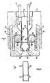
- Fig. 1 shows the perspective view of a connector 11 for establishing a releasable electrical connection.
- 12 is a carrier and guide element which can be fastened to a frame or a wiring printed circuit board via fastening tabs 13 and fastening holes 14.
- 15 are a plurality of connector pins, of which only the four delimiting pins are drawn. These connection pins can be designed to connect inserted, soldered, crimped or coiled connectors.
- Each connector pin 15 is connected to a contact element in the interior of the carrier and guide element 12, via which contact elements an electrical connection between the connector pins and the conductor tracks, for example a printed circuit board, can be established.
- the circuit board can be inserted into the connector from below, according to the position of the connector 11 shown.
- the carrier and guide element 12 guides the printed circuit board in such a way that the contact elements of the plug connector 11 make contact with one contact element of the printed circuit board, while all other possible connections are excluded by the guide as being faulty.
- 18 is a unit which is movably and captively attached to the carrier and guide element 12. It is referred to below as a power mediator.
- Fig. 2 shows a section across the connector in the direction of the arrow A of Fig. 1.
- 12 is again the support and guide element. It consists of non-conductive material and is made of plastic, for example, by injection molding.
- 18 is the power mediator. It also consists of non-conductive material, preferably of the same material as the carrier and guide element 12. Both parts 12 and 18 are captively connected to one another and can be displaced relative to one another in the direction of arrow B.
- connection pins 15 and 15 ' are rigidly connected to the carrier and guide element 12.
- the carrier and guide element is hollow inside.
- the cavity 20 serves to receive the contact side of a circuit board 22 to be contacted and also shown in FIG. 2.
- the contact elements already mentioned in connection with FIG. 1 are located in the cavity 20. 25 and 25 '. Each of these contact elements is connected to a respective connector pin 15 or 15 'via a conductive connection 26 or 26'.
- the contact elements 25 and 25 ' have good electrical conductivity and contact areas which point towards the interior of the cavity 20.
- the contact elements are weakly elastic. The elasticity serves to keep the contact elements in the direction of the double arrow C in a certain rest position. However, the elasticity does not serve to generate a contact force when the printed circuit board 22 is inserted.
- the carrier and guide element 12 carries profile surfaces 28 and 28 'on the inside. These profile surfaces are designed for carrying and guiding elastic force deflectors 30 and 30 '. These force deflectors have a cylindrical shape, for example, and are made of rubber-elastic material. Fig. 3 shows such a power deflector in a perspective view.
- the force mediator 18 has guides 34 and 34', locking hooks 36 and 36 'and a funnel-shaped opening 38.
- the guides 34 and 34 ' hold the first contact elements 25 and 25' in a position that ensures that a printed circuit board 22 can be freely inserted through the opening 38, that the printed circuit board cannot get caught anywhere when inserted, and that the first contact elements 25 and 25 'are always electrically insulated from one another.
- the locking hooks 36 and 36 ' are designed such that when the force mediator 18 is pushed together with the carrier and guide element 12, they snap into associated openings 40 and 40' of the carrier and guide element 12, respectively.
- the circuit board 22 is inserted into the plug connector 11.
- the circuit board 22 is inserted into the opening 38 with its contact elements 42 and 42 ′ to be contacted, which are attached on both sides of the circuit board 22. No forces occur here.
- a pressure edge 44 for example an incision in the plate 22, touches a pressure surface 45 on the force transmitter 18 which is assigned to this pressure edge the profile surfaces 28 and 32 and 28 'and 32' pressed.
- the force deflectors When the pressure is increased, the force deflectors deform due to their rubber elasticity so that there is a surface and non-positive contact between the profile surfaces mentioned and the force deflectors. Since rubber-elastic material does not change its volume when pressed together, the material of the force deflectors 30 and 30 'must deflect in the direction of the first contact elements 25 and 25'. As a result, these contact elements are pressed against the second contact elements 42 or 42 ′ of the printed circuit board 22. At the same time, the locking hooks 36 and 36 'approach the openings 40 and 40', respectively. When these openings are reached, the locking hooks snap into the Open and hold the force mediator 18 against the reaction forces of the force deflector 30 and 30 'in the inserted position.
- the locking hooks 36 and 36 ' must be moved out of the openings 40 and 40'. This is advantageously done by an overtravel mechanism which responds when the circuit board 22 including the force mediator 18 is pushed in further in the direction of arrow B than described in the previous section. Since the overtravel mechanism as such is not part of the invention, it is not described in detail here.
- the first contact elements 25 and 25 ' are connected to the pins 15 and 15' via conductive connections 26 and 26 '. At their free end they are guided through the guides 34 and 34 '. Furthermore, they have a weak elastic behavior. According to these requirements, the contact elements can be designed as conductor tracks of an elastic, thin circuit board. In another embodiment, the contact elements are thin springs which are guided by grooves in the interior of the carrier and guide element 12 and are electrically insulated from one another.
- a rubber-elastic band with a circular cross-section is a rubber-elastic band with a circular cross-section.
- this band with a different cross section, for example with an oval, rectangular or trapezoidal cross section, etc.
- a composite material can be used, for example porous material such as cellular or cellular rubber with a non-porous sheathing , tubular material with open tube ends (Fig. 4), or tubular material in which the tube ends are closed and the tube interior is filled with gas or a liquid, etc.
- All of the force deflectors 30 enumerated in the last two sections have the property of exerting a force in the direction of arrow B (FIG. 2) and when guided by suitably designed profile surfaces 32; 32 'and 28; 28 'or counter bearing in the direction of arrows C or C' and press the contact elements together.
- the opposing forces are absorbed by the circuit board material of the circuit board 22 and by the profile surfaces 28, 28 ', 32 and 32' or the abutments.
- Fig. 6 shows such a semi-rigid power deflector. 12 is a section of the support and guide element, and 28 is an arcuate profile surface.
- the force deflector 25 is a section of a first contact element and 30.1 together with 30.2 the force deflector.
- 30.1 resembles a quarter segment of a tube, on one edge of which elastic material 30.2 is attached. If a force is exerted on this force deflector in the direction of arrow B, the force deflector shifts and presses with its elastic part 30.2 in direction C onto the first contact elements 25.
- the elastic tip 30.2 results in a resilient contact pressure.
- the circuit board 22 is equipped with contact elements 42 and 42 'which are arranged on two sides of the circuit board.
- contact elements 42 and 42 ' which are arranged on two sides of the circuit board.
- the contact elements can be designed in the form of contact pins which are connected laterally to the printed circuit board via a pin base.
- the plug connector can not only be used to produce plug contacts with a printed circuit board 22, but quite generally for contacting a large number of mechanically interconnected contact elements, i.e. a connector.
- the force in direction B is transmitted from the circuit board 22 via the force mediator 18 to the force deflectors 30 and 30 '. It does not speak against the principle described if the force in direction B is transmitted directly from the plate to be contacted to the force deflectors 30 and 30 '.
- an element corresponding to the force mediator 18 must be attached to the plate to be inserted. This element must have profile surfaces 32 and 32 'and have locking hooks 36 and 36' which, in accordance with the manner shown in FIG. 2, with the force deflectors 30; 30 ', the profile surfaces 28 28' and the openings 40; 40 'of the support and guide element 12 cooperate.
Landscapes
- Coupling Device And Connection With Printed Circuit (AREA)
Applications Claiming Priority (2)
| Application Number | Priority Date | Filing Date | Title |
|---|---|---|---|
| CH1332/79 | 1979-02-12 | ||
| CH133279 | 1979-02-12 |
Publications (2)
| Publication Number | Publication Date |
|---|---|
| EP0014511A1 true EP0014511A1 (fr) | 1980-08-20 |
| EP0014511B1 EP0014511B1 (fr) | 1983-05-11 |
Family
ID=4207989
Family Applications (1)
| Application Number | Title | Priority Date | Filing Date |
|---|---|---|---|
| EP19800200104 Expired EP0014511B1 (fr) | 1979-02-12 | 1980-02-07 | Connecteur à force d'insertion nulle pouvant établir une connexion électrique déconnectable |
Country Status (2)
| Country | Link |
|---|---|
| EP (1) | EP0014511B1 (fr) |
| DE (1) | DE3063010D1 (fr) |
Cited By (4)
| Publication number | Priority date | Publication date | Assignee | Title |
|---|---|---|---|---|
| EP0378284A1 (fr) * | 1989-01-12 | 1990-07-18 | KRONE Aktiengesellschaft | Dispositif à fiches pour la technique des télécommunications et des informations |
| TR24642A (tr) * | 1989-05-10 | 1992-01-01 | Unilever Nv | Agartma aktivasyonu ve agartici bilesimler |
| EP0896388A3 (fr) * | 1997-08-06 | 1999-12-22 | Robert Bosch Gmbh | Connecteur électrique |
| EP1760837A1 (fr) * | 2005-08-30 | 2007-03-07 | Kostal Kontakt Systeme GmbH | Connecteur électrique à force d' insertion nulle |
Citations (4)
| Publication number | Priority date | Publication date | Assignee | Title |
|---|---|---|---|---|
| FR1537456A (fr) * | 1967-09-20 | 1968-08-23 | Bautzen Waggonbau Veb | Dispositif de liaison électrique, en particulier pour câbles à plusieurs veines |
| US3594707A (en) * | 1969-10-20 | 1971-07-20 | William Donald Peterson | Circuit board with fluid pressurized insert strip |
| DE2247927A1 (de) * | 1971-10-01 | 1973-04-05 | Honeywell Bull Soc Ind | Verbinder fuer gedruckte schaltungskarten |
| US4023881A (en) * | 1975-09-12 | 1977-05-17 | Souriau Et Cie | Connectors |
-
1980
- 1980-02-07 DE DE8080200104T patent/DE3063010D1/de not_active Expired
- 1980-02-07 EP EP19800200104 patent/EP0014511B1/fr not_active Expired
Patent Citations (4)
| Publication number | Priority date | Publication date | Assignee | Title |
|---|---|---|---|---|
| FR1537456A (fr) * | 1967-09-20 | 1968-08-23 | Bautzen Waggonbau Veb | Dispositif de liaison électrique, en particulier pour câbles à plusieurs veines |
| US3594707A (en) * | 1969-10-20 | 1971-07-20 | William Donald Peterson | Circuit board with fluid pressurized insert strip |
| DE2247927A1 (de) * | 1971-10-01 | 1973-04-05 | Honeywell Bull Soc Ind | Verbinder fuer gedruckte schaltungskarten |
| US4023881A (en) * | 1975-09-12 | 1977-05-17 | Souriau Et Cie | Connectors |
Cited By (4)
| Publication number | Priority date | Publication date | Assignee | Title |
|---|---|---|---|---|
| EP0378284A1 (fr) * | 1989-01-12 | 1990-07-18 | KRONE Aktiengesellschaft | Dispositif à fiches pour la technique des télécommunications et des informations |
| TR24642A (tr) * | 1989-05-10 | 1992-01-01 | Unilever Nv | Agartma aktivasyonu ve agartici bilesimler |
| EP0896388A3 (fr) * | 1997-08-06 | 1999-12-22 | Robert Bosch Gmbh | Connecteur électrique |
| EP1760837A1 (fr) * | 2005-08-30 | 2007-03-07 | Kostal Kontakt Systeme GmbH | Connecteur électrique à force d' insertion nulle |
Also Published As
| Publication number | Publication date |
|---|---|
| DE3063010D1 (en) | 1983-06-16 |
| EP0014511B1 (fr) | 1983-05-11 |
Similar Documents
| Publication | Publication Date | Title |
|---|---|---|
| DE2828588C2 (de) | Elektrischer Steckverbinder für einen eingreifenden Kontakt | |
| DE102015104625B4 (de) | Leiteranschlussklemme | |
| DE102007059096B4 (de) | Elektrodenklemme zum elektrischen Kontaktieren einer Filmelektrode und einer Druckknopfelektrode | |
| DE102015107853A1 (de) | Leiteranschlussklemme | |
| EP2729992A1 (fr) | Ensemble de serrage d'une borne de connexion électrique | |
| DE2826978A1 (de) | Schraubenlose elektrische anschlussklemme | |
| DE102020105813A1 (de) | Federkraftklemmanschluss | |
| EP3782238A1 (fr) | Module de connecteur enfichable blindé pour un connecteur enfichable industriel modulaire | |
| EP3000153A1 (fr) | Cavalier enfichable comprenant des éléments en tôle superposés | |
| DE1615666C3 (de) | Elektrische Klemmhülse | |
| DE102009008932A1 (de) | Elektrische Anschlussklemme | |
| DE2328505C2 (de) | Elektrischer Verbinder zur elektrischen Verbindung wenigstens zweier Leitungsdrähte | |
| WO2018007129A1 (fr) | Contact électrique à grande puissance | |
| DE102008060282B4 (de) | Werkzeuglos betätigbare Federklemme für elektrische Leiter | |
| EP0014511B1 (fr) | Connecteur à force d'insertion nulle pouvant établir une connexion électrique déconnectable | |
| DE2911573C2 (de) | Elektrisches Kupplungsstück zum Verbinden zweier Steckverbinder | |
| DE202009002240U1 (de) | Elektrische Anschlussklemme | |
| EP4032149A1 (fr) | Borne pour mise en contact de broche de contact | |
| DE3625864A1 (de) | Elektrische kontaktvorrichtung | |
| DE3020990A1 (de) | Elektrische anschluss- oder verbindungsklemme fuer nicht abisolierte leitungsenden | |
| DE4319615C2 (de) | Elektrischer Schalter zum Schalten eines Elektromotors, insbesondere in einer elektrischen Zahnbürste | |
| DE2165940C2 (de) | Kontaktvorrichtung mit einander gegenüberstehend angeordneten Kontaktlamellen | |
| DE3219294A1 (de) | Schaltvorrichtung fuer elektrische schalter, vorzugsweise fuer installationszwecke | |
| DE2622323A1 (de) | Kontaktvorrichtung zum anschluss eines elektrischen leitungsendes | |
| DE8911218U1 (de) | Elektrisches Druckübertragungselement für eine Anschlußklemme |
Legal Events
| Date | Code | Title | Description |
|---|---|---|---|
| PUAI | Public reference made under article 153(3) epc to a published international application that has entered the european phase |
Free format text: ORIGINAL CODE: 0009012 |
|
| AK | Designated contracting states |
Designated state(s): BE DE FR GB IT NL |
|
| 17P | Request for examination filed |
Effective date: 19810115 |
|
| GRAA | (expected) grant |
Free format text: ORIGINAL CODE: 0009210 |
|
| AK | Designated contracting states |
Designated state(s): BE DE FR GB IT NL |
|
| PG25 | Lapsed in a contracting state [announced via postgrant information from national office to epo] |
Ref country code: NL Effective date: 19830511 Ref country code: IT Free format text: LAPSE BECAUSE OF FAILURE TO SUBMIT A TRANSLATION OF THE DESCRIPTION OR TO PAY THE FEE WITHIN THE PRESCRIBED TIME-LIMIT;WARNING: LAPSES OF ITALIAN PATENTS WITH EFFECTIVE DATE BEFORE 2007 MAY HAVE OCCURRED AT ANY TIME BEFORE 2007. THE CORRECT EFFECTIVE DATE MAY BE DIFFERENT FROM THE ONE RECORDED. Effective date: 19830511 Ref country code: FR Free format text: THE PATENT HAS BEEN ANNULLED BY A DECISION OF A NATIONAL AUTHORITY Effective date: 19830511 Ref country code: BE Effective date: 19830511 |
|
| REF | Corresponds to: |
Ref document number: 3063010 Country of ref document: DE Date of ref document: 19830616 |
|
| NLV1 | Nl: lapsed or annulled due to failure to fulfill the requirements of art. 29p and 29m of the patents act | ||
| EN | Fr: translation not filed | ||
| PLBE | No opposition filed within time limit |
Free format text: ORIGINAL CODE: 0009261 |
|
| STAA | Information on the status of an ep patent application or granted ep patent |
Free format text: STATUS: NO OPPOSITION FILED WITHIN TIME LIMIT |
|
| 26N | No opposition filed | ||
| GBPC | Gb: european patent ceased through non-payment of renewal fee | ||
| PG25 | Lapsed in a contracting state [announced via postgrant information from national office to epo] |
Ref country code: DE Effective date: 19841101 |
|
| PG25 | Lapsed in a contracting state [announced via postgrant information from national office to epo] |
Ref country code: GB Effective date: 19881118 |