EP0014945A1 - Montage pour la production d'une fréquence d'horloge dans des centraux de télécommunication, en particulier dans des centraux à multiplexage temporel de signaux numériques - Google Patents
Montage pour la production d'une fréquence d'horloge dans des centraux de télécommunication, en particulier dans des centraux à multiplexage temporel de signaux numériques Download PDFInfo
- Publication number
- EP0014945A1 EP0014945A1 EP80100711A EP80100711A EP0014945A1 EP 0014945 A1 EP0014945 A1 EP 0014945A1 EP 80100711 A EP80100711 A EP 80100711A EP 80100711 A EP80100711 A EP 80100711A EP 0014945 A1 EP0014945 A1 EP 0014945A1
- Authority
- EP
- European Patent Office
- Prior art keywords
- clock
- official
- ccg
- frequency
- phase
- Prior art date
- Legal status (The legal status is an assumption and is not a legal conclusion. Google has not performed a legal analysis and makes no representation as to the accuracy of the status listed.)
- Granted
Links
- 230000009467 reduction Effects 0.000 claims abstract description 17
- 239000003638 chemical reducing agent Substances 0.000 claims abstract description 16
- 238000000034 method Methods 0.000 claims description 7
- 230000001360 synchronised effect Effects 0.000 claims description 7
- 230000010363 phase shift Effects 0.000 claims description 4
- 230000003111 delayed effect Effects 0.000 claims 1
- 230000004913 activation Effects 0.000 description 5
- 230000000694 effects Effects 0.000 description 4
- 230000008901 benefit Effects 0.000 description 3
- 238000010586 diagram Methods 0.000 description 2
- 230000002035 prolonged effect Effects 0.000 description 2
- 230000000717 retained effect Effects 0.000 description 2
- 102100021606 Ephrin type-A receptor 7 Human genes 0.000 description 1
- 101710116633 Ephrin type-A receptor 7 Proteins 0.000 description 1
- 230000005540 biological transmission Effects 0.000 description 1
- 238000004891 communication Methods 0.000 description 1
- 238000012937 correction Methods 0.000 description 1
- 238000011161 development Methods 0.000 description 1
- 238000012423 maintenance Methods 0.000 description 1
- 239000011159 matrix material Substances 0.000 description 1
- 230000001404 mediated effect Effects 0.000 description 1
- 230000008569 process Effects 0.000 description 1
- 230000004044 response Effects 0.000 description 1
- 238000004904 shortening Methods 0.000 description 1
- 230000001960 triggered effect Effects 0.000 description 1
Images


Classifications
-
- H—ELECTRICITY
- H04—ELECTRIC COMMUNICATION TECHNIQUE
- H04Q—SELECTING
- H04Q11/00—Selecting arrangements for multiplex systems
- H04Q11/04—Selecting arrangements for multiplex systems for time-division multiplexing
-
- H—ELECTRICITY
- H04—ELECTRIC COMMUNICATION TECHNIQUE
- H04J—MULTIPLEX COMMUNICATION
- H04J3/00—Time-division multiplex systems
- H04J3/02—Details
- H04J3/06—Synchronising arrangements
- H04J3/0635—Clock or time synchronisation in a network
- H04J3/0685—Clock or time synchronisation in a node; Intranode synchronisation
- H04J3/0688—Change of the master or reference, e.g. take-over or failure of the master
Definitions
- a coarse adjustment digital phase locked loop is formed, the mitzugie per beat period between normal frequency and reference frequency Henden oscillator emits only a digital control step for frequency correction and that in addition an analog phase locked loop is provided, the pull range corresponds to about twice the control step of the digital control loop, and that the middle of the analog control range in the middle between the two response points of the digital control loop associated with a beat period lies and that when the analog control range is exceeded, a further control step is triggered by the digital control loop, which causes the phase of the reference frequency of the oscillator to be pulled back to return approximately to the middle of the control range of the analog phase control, and that the control variable thus formed is stored .
- the stored controlled variable is retained in the event of a failure of the normal frequency (see also tekade techn.mitt. (1978), pp. 24-28), so that interruptions in the normal frequency transmission have no influence on the short-term frequency stability of the oscillator ; in the event of a failure of the frequency readjustment device, however, frequency stability is no longer ensured.
- the office clocks generated in the two office clock generation arrangements are practically in phase, so that when the bit streams mediated via the two switching matrix halves are merged, negligibly small phase differences occur between the two bit streams and there is a mutual switching of the office clock generation arrangements, on account of which a now leading office clock generation system works (and vice versa), at most there is a limited phase shift which leaves the synchronism of line regenerators inserted in the lines coming from the switching system unaffected.
- the possibility is opened to supply both switching network halves with clocks after a corresponding substitute circuit in the event of a fault or during maintenance-related interventions while avoiding impermissible phase jumps 'can.
- the master clock is only supplied to one of the two office clock generators during servo synchronization.
- the circuit redundancy and, in the case of duplicate office clock generation arrangements, frequency synchronization of both office clock generators from different master clock sources using the servo synchronous method, the task is to limit deviations from the desired phase equality of the two office clocks to a maximum permitted value even if the two office clock generators supplied master clocks (in themselves the same clock frequency) can differ in their phase position by up to 2 ⁇ .
- the invention has the advantage that the phase difference between the office clocks supplied by the two office clock producers does not exceed an amount in the order of the intermediate clock period, so that the phase difference between the be iden by appropriate specification of the intermediate clock frequency. Office clocks can be kept within the desired limits.
- the invention also has the advantage that a retraction of the office clock generator in each case is not effected even with an arbitrarily small phase difference, rather the phase synchronization is subject to a hysteresis, due to which a jitter of the leading office clock remains irrelevant.
- the master clock pulses are expediently fed to the two office clock generators by a frequency readjustment device which is acted upon by a normal clock pulse and at the same time stores the respective controlled variable;
- a frequency readjustment device which is acted upon by a normal clock pulse and at the same time stores the respective controlled variable;
- a digital clock reduction and phase synchronization circuit is expediently connected to the intermediate clock generator, which is servo-synchronized by the master clock, of the office clock generator in each case carried out, with a comparison input is connected to the output of the leading public clock generator and at the output of the official clock of the managed official clock generator occurs; this allows a phase synchronization between the leading and leading office clock without an intervention in the actual intermediate clock generator of the office clock generator being carried out.
- the invention can expediently experience a further embodiment in such a way that the digital clock reduction and phase synchronization circuit has an intermediate clock frequency halving stage, which operates a phase shift key operated by each time a phase difference exceeding the respective limit value is detected, an additional reduction step only with a subsequent leading official clock Frequency converter is connected downstream, with the output of the official clock output of the official clock generator corresponding to the official clock frequency.
- two link elements to which the respective clock input of the leading office clock generator is applied at their second input, the bistable flip-flop flip-flops and an OR circuit to one controlling the frequency reducer can be connected to the frequency reducer via two office clock time slot circuits Guide the setting element whose output is also connected to an actuator for the phase switch.
- the setting member has a lock input for a changeover signal for switching over a previously performed official clock generator into a leading official clock generator.
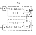
- the drawing Fig. 1 shows schematically an embodiment of a. Circuit arrangement for clock generation with a doubly provided official clock generator arrangement CCG ', CCG "according to the invention.
- One of the two official clock generators for example the official clock generator CCG', may have at its clock output T 'an official clock generated by it independently of the other official clock generator CCG" with a clock frequency of, for example, 2.048 MHz; the official clock generator CCG "may supply an official clock of the same frequency that is synchronized at least approximately in phase with the official clock supplied by the official clock generator CCG '.
- Such frequency control devices which essentially have a PLL oscillator and one S p ei- Rather, for the respective controlled variable in which the respectively stored controlled variable is retained in the event of a failure of the normal cycle, are generally known (for example from DE-AS 26 36 150), which is why further explanations are unnecessary here; Suffice it to say here that such frequency readjustment devices are able to guarantee a required frequency tolerance of the button clocks M ', M "of 10 -9 / d.
- the normal clock N in turn can originate directly from a central normal clock generator to which a multiplicity of identical or similar circuit arrangements are connected in parallel; however, the normal clock N can also be derived from a central normal clock generator via a chain connection of clock generators or frequency control circuits operated in each case by a master slave.
- phase of the two master clocks M 'and M can differ by up to 2 ⁇ (corresponding to 488ns with a master clock frequency of 2.048 MEz). So that there is nevertheless a phase difference between the two official clocks T' and T" within the desired limits of, for example, 35 ns holds, both the leading official clock generator CCG 'and the official clock generator CCG' he is running, servo-synchronized by the respectively supplied master clock M 'or M', generate an intermediate clock H 'or H' with a clock period h (in FIG. 3 and Fig.
- FIG. 2 An example of how the digital clock reduction and phase synchronization circuit UVR can advantageously be designed is shown in the drawing in FIG. 2;
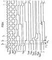
- the mode of operation of the circuit arrangement according to FIG. 2 is illustrated by the switching state diagrams shown in the drawings in FIGS. 3 and 4.
- this leads to the intermediate clock frequency of, for example, 32.768 MHz having intermediate clock, as shown in Fig. 3 and Fig. 4 in line H ", applied intermediate clock input H" initially to an intermediate clock frequency halving stage in the form of a bistable flip-flop BKU, the switching states in Fig. 3 and Fig. 4 in each Line Q BKU are clarified.
- the intermediate clock frequency halving stage BKU is followed by a further frequency reducer U, which can be formed by a binary counter and with which the official clock frequency of 2.048 MHz in the example corresponding output c is connected via a bistable flip-flop BKT to the official clock output T '' of the official clock generator.
- Input signals and switching states of the bistable switching element BKP are indicated in FIG. 3 and FIG. 4 in lines J BKP and Q BKP , switching states of frequency reducer U in lines a, b, c. In each case in line T "in FIG. 3 and FIG. 4 the official clock occurring at the official clock output T" of the circuit arrangement according to FIG. 2 is shown.
- a phase comparison circuit for the phase comparison between the guided office clock T "and the leading office clock supplied via a line T ', as shown in FIG. 3 and FIG . 4 in line T', is connected to the frequency reducer U.
- This comparison circuit initially has two time window circuits, which are formed by a NAND gate UG3 and a bistable flip-flop BK3 and a bistable flip-flop BK4; switching states of the two bistable flip-flops are shown in FIGS. 3 and 4 in lines Q BK3 and Q BK4 .
- the two bistable flip-flops BK3 and BK4 each lead to one input of two logic elements, namely the NOR gate UGN and the AND gate UGV, each of which has the official clock T 'at its second input.
- bistable flip-flops BKN or BKV, BEVv the switching states of which are shown in FIGS. 3 and 4 in the lines Q BKN , Q BKV , Q BKVv and which are combined to form an OR circuit a bistable flip-flop BKR.
- This bistable flip-flop BKR is connected on the one hand with a special switching input of the frequency converter U and on the other hand an actuator for the phase switch EOP provided by a bistable flip-flop BKS.
- the switching states of the last two bistable flip-flops are shown in FIGS. 3 and 4 in lines Q BKR and Q BKS .
- Figure 2 is where in turn the indices indicate the corresponding circuit components; in practice, about be.
- the limit values ⁇ Nmax and ⁇ Vmax are both in the order of an intermediate clock period h of 30.52 ns and in the example. in any case below the maximum permitted phase difference between the leading clock pulse T 'and the official clock T', of 35 ns in the example.
- bistable flip-flop BKN Both the activation of the bistable flip-flop BKN and the activation of the bistable flip-flop BKV or BEVv result in an activation of the following bistable flip-flop BKR, the bistable flip-flop BKR being reset again after two intermediate cycle periods via the bistable flip-flops EK11 and BK12; at the same time, the bistable flip-flop BKS is also switched over.
- the latter has the result that the frequency converter U is now supplied with a clock inverse to the previous clock via the phase switch EOP, which has an immediate effect on the lengthening of the currently occurring eleven period of the official clock T "by the duration h of a period of the intermediate clock H". how this is provided with the leading official clock T "and indicated for this purpose in line 4" in FIG. 4.
- the activation of the bistable flip-flop BKR in the circuit arrangement according to FIG. 2 also has the consequence that the frequency reducer U which can be implemented by a binary counter at time t z , ie to the positive clock edge of the intermediate clock H "occurring during the activation of the bistable flip-flop BKR the reduction state corresponding to the counting state 2.
- the frequency reducer U arrives in this reduction state at this instant with the leading office clock pulse T "(FIG. 4) so that the setting process has no further effects. If the official clock T "lagged (FIG. 3), the frequency reducer at the time t z (in FIG.
- the guided office clock T "follows the leading office clock T 'in the phase position.
- the phase synchronization is subject to a certain hysteresis, so that jitter phenomena of the leading office clock T', as they occur in practice with time amplitudes, are of the order of magnitude of 5 ns can remain irrelevant
- the hysteresis range results from FIGS. 3 and 4 with in practice, about be.
- the circuit arrangement according to FIG. 2 also has a changeover signal input FG, which leads to a lock input of the bistable Xipp element BKR. Via this change-over signal input, a change-over signal "0" occurring synchronously with the official clock can be used to switch over the previous official clock generator, so that it is no longer operated in accordance with the official clock occurring on line T ';
- the official clock generator CCG " in Fig. 1), if necessary, in turn to lead the previously leading official clock generator (CCG 'in Fig. 1), which has been switched in the opposite direction, as is indicated in Fig. 1 by a dashed line.
Landscapes
- Engineering & Computer Science (AREA)
- Computer Networks & Wireless Communication (AREA)
- Signal Processing (AREA)
- Stabilization Of Oscillater, Synchronisation, Frequency Synthesizers (AREA)
- Synchronisation In Digital Transmission Systems (AREA)
- Exchange Systems With Centralized Control (AREA)
- Mobile Radio Communication Systems (AREA)
- Time-Division Multiplex Systems (AREA)
Priority Applications (1)
| Application Number | Priority Date | Filing Date | Title |
|---|---|---|---|
| AT80100711T ATE3606T1 (de) | 1979-02-27 | 1980-02-12 | Schaltungsanordnung zur takterzeugung in fernmeldeanlagen, insbesondere zeitmultiplexdigital-vermittlungsanlagen. |
Applications Claiming Priority (2)
| Application Number | Priority Date | Filing Date | Title |
|---|---|---|---|
| DE2907608 | 1979-02-27 | ||
| DE19792907608 DE2907608A1 (de) | 1979-02-27 | 1979-02-27 | Schaltungsanordnung zur takterzeugung in fernmeldeanlagen, insbesondere zeitmultiplex-digital-vermittlungsanlagen |
Publications (2)
| Publication Number | Publication Date |
|---|---|
| EP0014945A1 true EP0014945A1 (fr) | 1980-09-03 |
| EP0014945B1 EP0014945B1 (fr) | 1983-05-25 |
Family
ID=6064011
Family Applications (1)
| Application Number | Title | Priority Date | Filing Date |
|---|---|---|---|
| EP80100711A Expired EP0014945B1 (fr) | 1979-02-27 | 1980-02-12 | Montage pour la production d'une fréquence d'horloge dans des centraux de télécommunication, en particulier dans des centraux à multiplexage temporel de signaux numériques |
Country Status (7)
| Country | Link |
|---|---|
| US (1) | US4330854A (fr) |
| EP (1) | EP0014945B1 (fr) |
| JP (1) | JPS55117349A (fr) |
| AT (1) | ATE3606T1 (fr) |
| DE (2) | DE2907608A1 (fr) |
| IL (1) | IL59468A (fr) |
| ZA (1) | ZA801100B (fr) |
Cited By (6)
| Publication number | Priority date | Publication date | Assignee | Title |
|---|---|---|---|---|
| DE3207245A1 (de) * | 1982-02-25 | 1983-09-01 | Deutsche Telephonwerke Und Kabelindustrie Ag, 1000 Berlin | Verfahren und schaltungsanordnung zur phasenrichtigen takterzeugung in digitalen kommunikationssystemen, z.b. fernsprechvermittlungsanlagen |
| EP0110648A1 (fr) * | 1982-11-26 | 1984-06-13 | Fujitsu Limited | Appareil de synchronisation dans un équipement redondant de communication à accès multiple par répartition dans le temps |
| EP0389662A1 (fr) * | 1989-03-31 | 1990-10-03 | Siemens Aktiengesellschaft | Procédé de réglage de la phase des signaux de deux générateurs d'horloge dans les réseaux de télécommunications |
| AU610783B1 (en) * | 1989-09-27 | 1991-05-23 | Siemens Aktiengesellschaft | Clock supply for multiplex systems |
| WO1998027680A1 (fr) * | 1996-12-19 | 1998-06-25 | Dsc Telecom L.P. | Dispositif et procede pour l'alignement et la commutation d'horloge |
| DE19947095A1 (de) * | 1999-09-30 | 2001-05-03 | Siemens Ag | Vorrichtung zur Synchronisierung des Rahmentaktes in Einheiten/Knoten datenübertragender Systeme |
Families Citing this family (8)
| Publication number | Priority date | Publication date | Assignee | Title |
|---|---|---|---|---|
| DE3227848A1 (de) * | 1982-07-26 | 1984-01-26 | Siemens AG, 1000 Berlin und 8000 München | Schaltungsanordnung zur takterzeugung in fernmeldeanlagen, insbesondere zeitmultiplex-digital-vermittlungsanlagen |
| DE3227849A1 (de) * | 1982-07-26 | 1984-01-26 | Siemens AG, 1000 Berlin und 8000 München | Schaltungsanordnung zur takterzeugung in fernmeldeanlagen, insbesondere zeitmultiplex-digital-vermittlungsanlagen |
| JPS59106261U (ja) * | 1982-12-29 | 1984-07-17 | 日本電気株式会社 | トリガ−回路 |
| US4583054A (en) * | 1984-11-13 | 1986-04-15 | Rca Corporation | Frequency time standard failure monitor |
| US4860285A (en) * | 1987-10-21 | 1989-08-22 | Advanced Micro Devices, Inc. | Master/slave synchronizer |
| US5391996A (en) * | 1993-11-19 | 1995-02-21 | General Instrument Corporation Of Delaware | Techniques for generating two high frequency signals with a constant phase difference over a wide frequency band |
| US5631933A (en) * | 1996-02-21 | 1997-05-20 | Hewlett-Packard Company | Phase-locked digital synthesizers |
| US6297702B1 (en) * | 2000-01-10 | 2001-10-02 | Honeywell International Inc. | Phase lock loop system and method |
Citations (6)
| Publication number | Priority date | Publication date | Assignee | Title |
|---|---|---|---|---|
| US3522455A (en) * | 1967-07-27 | 1970-08-04 | Bendix Corp | Method and means of synchronizing timing pulses of a three channel triplicated system |
| GB1350150A (en) * | 1970-11-20 | 1974-04-18 | Ericsson Telefon Ab L M | Computer control |
| GB1444067A (en) * | 1973-07-13 | 1976-07-28 | Int Standard Electric Corp | Control arrangement |
| US3974333A (en) * | 1975-09-24 | 1976-08-10 | Bell Telephone Laboratories, Incorporated | Adaptive synchronization system |
| DE2636150B1 (de) * | 1976-08-11 | 1978-01-05 | Siemens Ag | Verfahren und anordnung zur phasengenauen synchronisation von grundgeneratoren |
| LU80132A1 (fr) * | 1977-08-22 | 1979-01-19 |
Family Cites Families (1)
| Publication number | Priority date | Publication date | Assignee | Title |
|---|---|---|---|---|
| US3803568A (en) * | 1973-04-06 | 1974-04-09 | Gte Automatic Electric Lab Inc | System clock for electronic communication systems |
-
1979
- 1979-02-27 DE DE19792907608 patent/DE2907608A1/de not_active Withdrawn
-
1980
- 1980-02-12 US US06/120,910 patent/US4330854A/en not_active Expired - Lifetime
- 1980-02-12 AT AT80100711T patent/ATE3606T1/de not_active IP Right Cessation
- 1980-02-12 EP EP80100711A patent/EP0014945B1/fr not_active Expired
- 1980-02-12 DE DE8080100711T patent/DE3063404D1/de not_active Expired
- 1980-02-25 IL IL59468A patent/IL59468A/xx unknown
- 1980-02-26 ZA ZA00801100A patent/ZA801100B/xx unknown
- 1980-02-27 JP JP2289180A patent/JPS55117349A/ja active Pending
Patent Citations (7)
| Publication number | Priority date | Publication date | Assignee | Title |
|---|---|---|---|---|
| US3522455A (en) * | 1967-07-27 | 1970-08-04 | Bendix Corp | Method and means of synchronizing timing pulses of a three channel triplicated system |
| GB1350150A (en) * | 1970-11-20 | 1974-04-18 | Ericsson Telefon Ab L M | Computer control |
| GB1444067A (en) * | 1973-07-13 | 1976-07-28 | Int Standard Electric Corp | Control arrangement |
| US3974333A (en) * | 1975-09-24 | 1976-08-10 | Bell Telephone Laboratories, Incorporated | Adaptive synchronization system |
| DE2636150B1 (de) * | 1976-08-11 | 1978-01-05 | Siemens Ag | Verfahren und anordnung zur phasengenauen synchronisation von grundgeneratoren |
| LU80132A1 (fr) * | 1977-08-22 | 1979-01-19 | ||
| DE2737713A1 (de) * | 1977-08-22 | 1979-03-08 | Siemens Ag | Zeitmultiplex-digital-vermittlungsanlage, insbesondere pcm-fernsprechvermittlungsanlage, mit doppelt vorgesehenen koppelfeldeinrichtungen |
Non-Patent Citations (2)
| Title |
|---|
| ELEKTRONIK, Band 22, Nr. 8, August 1973, Seiten 285-287 Munchen, DE. GROSSKOPF: "Rechteckgenerator mit digital einstellbarer Frequenz" * Seite 285, linke Spalte, Zeilen 1-28 * * |
| HAZELTINE LABORATORIES STAFF, "Principles of Color Television", 1956, Wiley, Seiten 180-190 New York, U.S.A. * Seite 180, Zeile 7 - Seite 181, Zeile 19 * * |
Cited By (8)
| Publication number | Priority date | Publication date | Assignee | Title |
|---|---|---|---|---|
| DE3207245A1 (de) * | 1982-02-25 | 1983-09-01 | Deutsche Telephonwerke Und Kabelindustrie Ag, 1000 Berlin | Verfahren und schaltungsanordnung zur phasenrichtigen takterzeugung in digitalen kommunikationssystemen, z.b. fernsprechvermittlungsanlagen |
| EP0110648A1 (fr) * | 1982-11-26 | 1984-06-13 | Fujitsu Limited | Appareil de synchronisation dans un équipement redondant de communication à accès multiple par répartition dans le temps |
| US4574377A (en) * | 1982-11-26 | 1986-03-04 | Fujitsu Limited | Synchronization method and apparatus in redundant time-division-multiple-access communication equipment |
| EP0389662A1 (fr) * | 1989-03-31 | 1990-10-03 | Siemens Aktiengesellschaft | Procédé de réglage de la phase des signaux de deux générateurs d'horloge dans les réseaux de télécommunications |
| AU610783B1 (en) * | 1989-09-27 | 1991-05-23 | Siemens Aktiengesellschaft | Clock supply for multiplex systems |
| WO1998027680A1 (fr) * | 1996-12-19 | 1998-06-25 | Dsc Telecom L.P. | Dispositif et procede pour l'alignement et la commutation d'horloge |
| DE19947095A1 (de) * | 1999-09-30 | 2001-05-03 | Siemens Ag | Vorrichtung zur Synchronisierung des Rahmentaktes in Einheiten/Knoten datenübertragender Systeme |
| US6778623B1 (en) | 1999-09-30 | 2004-08-17 | Siemens Aktiengesellschaft | Apparatus for synchronizing the frame clock in units/nodes of data-transmitting systems |
Also Published As
| Publication number | Publication date |
|---|---|
| US4330854A (en) | 1982-05-18 |
| EP0014945B1 (fr) | 1983-05-25 |
| JPS55117349A (en) | 1980-09-09 |
| DE2907608A1 (de) | 1980-08-28 |
| ATE3606T1 (de) | 1983-06-15 |
| DE3063404D1 (en) | 1983-07-07 |
| IL59468A (en) | 1982-11-30 |
| ZA801100B (en) | 1981-03-25 |
| IL59468A0 (en) | 1980-05-30 |
Similar Documents
| Publication | Publication Date | Title |
|---|---|---|
| DE3687896T2 (de) | Phasenanpassungssystem. | |
| EP0014945B1 (fr) | Montage pour la production d'une fréquence d'horloge dans des centraux de télécommunication, en particulier dans des centraux à multiplexage temporel de signaux numériques | |
| DE69737903T2 (de) | Verfahren und Vorrichtung für eine störungsfreie Umschaltung zwischen redundanten Signalen | |
| LU87892A1 (de) | Optisches datennetz hoher betriebssicherheit | |
| DE2428495A1 (de) | Anordnung zur stoerungsunterdrueckung in synchronisierten oszillatoren | |
| DE3222993A1 (de) | Funk-synchronisationssystem | |
| DE3215783C2 (de) | Digitale Datenübertragungsanlage mit störungsfreiem Umschalten von regulären Kanälen auf einen Reservekanal | |
| DE19901588A1 (de) | Synchronisation eines Netzelementes in einem synchronen digitalen Nachrichtenübertragungsnetz | |
| DE2951781C2 (fr) | ||
| DE2819519C2 (de) | Taktgeber | |
| DE2149911B2 (de) | Schaltungsanordnung zur gegenseitigen synchronisierung der in den vermittlungsstellen eines pcm-zeitmultiplexfernmeldenetzes vorgesehenen amtstaktoszillatoren | |
| DE2752996A1 (de) | Digitale multiplexiervorrichtung fuer plesiochrone bitfolgen | |
| DE60035373T2 (de) | Vorrichtung und verfahren in einer halbleiterschaltung | |
| EP0100076B1 (fr) | Arrangement pour la génération de signaux d'horloge dans des installations de télécommunication, en particulier des centraux numériques temporels | |
| DE2655443B2 (de) | Vervielfachte Zeitsteuerung zum Erzeugen von Zeitsignalen für Installationen mit signalverarbeitenden Schaltungen | |
| DE3340553C2 (fr) | ||
| EP1223698B1 (fr) | Procédé et module de compensation de phase des signaux d'horloge | |
| DE2737713C2 (de) | Zeitmultiplex-Digital-Vermittlungsanlage, insbesondere PCM-Fernsprechvermittlungsanlage, mit doppelt vorgesehenen Koppelfeldeinrichtungen | |
| DE3227849C2 (fr) | ||
| EP1094610A1 (fr) | Boucle de verrouillage de phase numérique | |
| DE3809089C2 (fr) | ||
| DE19943172A1 (de) | Anordnung zur Taktversorgung von hochbitratigen Koppelfeldstrukturen | |
| DE19618953C2 (de) | Synchroner Taktschaltkreis | |
| DE3924907A1 (de) | Redundante taktgeberanordnung | |
| DE3835259C2 (de) | Schaltungsanordnung zum Empfang von seriell übertragenen digitalen Daten |
Legal Events
| Date | Code | Title | Description |
|---|---|---|---|
| PUAI | Public reference made under article 153(3) epc to a published international application that has entered the european phase |
Free format text: ORIGINAL CODE: 0009012 |
|
| AK | Designated contracting states |
Designated state(s): AT CH DE FR GB IT NL SE |
|
| 17P | Request for examination filed |
Effective date: 19810213 |
|
| ITF | It: translation for a ep patent filed | ||
| GRAA | (expected) grant |
Free format text: ORIGINAL CODE: 0009210 |
|
| AK | Designated contracting states |
Designated state(s): AT CH DE FR GB IT NL SE |
|
| REF | Corresponds to: |
Ref document number: 3606 Country of ref document: AT Date of ref document: 19830615 Kind code of ref document: T |
|
| REF | Corresponds to: |
Ref document number: 3063404 Country of ref document: DE Date of ref document: 19830707 |
|
| ET | Fr: translation filed | ||
| PLBE | No opposition filed within time limit |
Free format text: ORIGINAL CODE: 0009261 |
|
| STAA | Information on the status of an ep patent application or granted ep patent |
Free format text: STATUS: NO OPPOSITION FILED WITHIN TIME LIMIT |
|
| 26N | No opposition filed | ||
| ITTA | It: last paid annual fee | ||
| PGFP | Annual fee paid to national office [announced via postgrant information from national office to epo] |
Ref country code: CH Payment date: 19930519 Year of fee payment: 14 |
|
| PGFP | Annual fee paid to national office [announced via postgrant information from national office to epo] |
Ref country code: GB Payment date: 19940124 Year of fee payment: 15 |
|
| PGFP | Annual fee paid to national office [announced via postgrant information from national office to epo] |
Ref country code: AT Payment date: 19940128 Year of fee payment: 15 |
|
| PGFP | Annual fee paid to national office [announced via postgrant information from national office to epo] |
Ref country code: SE Payment date: 19940223 Year of fee payment: 15 |
|
| PGFP | Annual fee paid to national office [announced via postgrant information from national office to epo] |
Ref country code: FR Payment date: 19940224 Year of fee payment: 15 |
|
| PG25 | Lapsed in a contracting state [announced via postgrant information from national office to epo] |
Ref country code: CH Effective date: 19940228 |
|
| PGFP | Annual fee paid to national office [announced via postgrant information from national office to epo] |
Ref country code: NL Payment date: 19940228 Year of fee payment: 15 |
|
| REG | Reference to a national code |
Ref country code: CH Ref legal event code: PL |
|
| EAL | Se: european patent in force in sweden |
Ref document number: 80100711.3 |
|
| PG25 | Lapsed in a contracting state [announced via postgrant information from national office to epo] |
Ref country code: GB Effective date: 19950212 Ref country code: AT Effective date: 19950212 |
|
| PG25 | Lapsed in a contracting state [announced via postgrant information from national office to epo] |
Ref country code: SE Effective date: 19950213 |
|
| PG25 | Lapsed in a contracting state [announced via postgrant information from national office to epo] |
Ref country code: NL Effective date: 19950901 |
|
| GBPC | Gb: european patent ceased through non-payment of renewal fee |
Effective date: 19950212 |
|
| PG25 | Lapsed in a contracting state [announced via postgrant information from national office to epo] |
Ref country code: FR Effective date: 19951031 |
|
| NLV4 | Nl: lapsed or anulled due to non-payment of the annual fee |
Effective date: 19950901 |
|
| EUG | Se: european patent has lapsed |
Ref document number: 80100711.3 |
|
| REG | Reference to a national code |
Ref country code: FR Ref legal event code: ST |
|
| PGFP | Annual fee paid to national office [announced via postgrant information from national office to epo] |
Ref country code: DE Payment date: 19970418 Year of fee payment: 18 |
|
| PG25 | Lapsed in a contracting state [announced via postgrant information from national office to epo] |
Ref country code: DE Free format text: LAPSE BECAUSE OF NON-PAYMENT OF DUE FEES Effective date: 19981103 |