EP0016251A1 - Circuit électronique à film mince et procédé pour sa fabrication - Google Patents
Circuit électronique à film mince et procédé pour sa fabrication Download PDFInfo
- Publication number
- EP0016251A1 EP0016251A1 EP79104498A EP79104498A EP0016251A1 EP 0016251 A1 EP0016251 A1 EP 0016251A1 EP 79104498 A EP79104498 A EP 79104498A EP 79104498 A EP79104498 A EP 79104498A EP 0016251 A1 EP0016251 A1 EP 0016251A1
- Authority
- EP
- European Patent Office
- Prior art keywords
- layer
- nickel
- valve metal
- pattern
- electronic thin
- Prior art date
- Legal status (The legal status is an assumption and is not a legal conclusion. Google has not performed a legal analysis and makes no representation as to the accuracy of the status listed.)
- Granted
Links
Images


Classifications
-
- H—ELECTRICITY
- H10—SEMICONDUCTOR DEVICES; ELECTRIC SOLID-STATE DEVICES NOT OTHERWISE PROVIDED FOR
- H10D—INORGANIC ELECTRIC SEMICONDUCTOR DEVICES
- H10D86/00—Integrated devices formed in or on insulating or conducting substrates, e.g. formed in silicon-on-insulator [SOI] substrates or on stainless steel or glass substrates
- H10D86/80—Integrated devices formed in or on insulating or conducting substrates, e.g. formed in silicon-on-insulator [SOI] substrates or on stainless steel or glass substrates characterised by multiple passive components, e.g. resistors, capacitors or inductors
- H10D86/85—Integrated devices formed in or on insulating or conducting substrates, e.g. formed in silicon-on-insulator [SOI] substrates or on stainless steel or glass substrates characterised by multiple passive components, e.g. resistors, capacitors or inductors characterised by only passive components
-
- Y—GENERAL TAGGING OF NEW TECHNOLOGICAL DEVELOPMENTS; GENERAL TAGGING OF CROSS-SECTIONAL TECHNOLOGIES SPANNING OVER SEVERAL SECTIONS OF THE IPC; TECHNICAL SUBJECTS COVERED BY FORMER USPC CROSS-REFERENCE ART COLLECTIONS [XRACs] AND DIGESTS
- Y10—TECHNICAL SUBJECTS COVERED BY FORMER USPC
- Y10T—TECHNICAL SUBJECTS COVERED BY FORMER US CLASSIFICATION
- Y10T29/00—Metal working
- Y10T29/49—Method of mechanical manufacture
- Y10T29/49002—Electrical device making
- Y10T29/49082—Resistor making
- Y10T29/49099—Coating resistive material on a base
-
- Y—GENERAL TAGGING OF NEW TECHNOLOGICAL DEVELOPMENTS; GENERAL TAGGING OF CROSS-SECTIONAL TECHNOLOGIES SPANNING OVER SEVERAL SECTIONS OF THE IPC; TECHNICAL SUBJECTS COVERED BY FORMER USPC CROSS-REFERENCE ART COLLECTIONS [XRACs] AND DIGESTS
- Y10—TECHNICAL SUBJECTS COVERED BY FORMER USPC
- Y10T—TECHNICAL SUBJECTS COVERED BY FORMER US CLASSIFICATION
- Y10T29/00—Metal working
- Y10T29/49—Method of mechanical manufacture
- Y10T29/49002—Electrical device making
- Y10T29/49082—Resistor making
- Y10T29/49101—Applying terminal
-
- Y—GENERAL TAGGING OF NEW TECHNOLOGICAL DEVELOPMENTS; GENERAL TAGGING OF CROSS-SECTIONAL TECHNOLOGIES SPANNING OVER SEVERAL SECTIONS OF THE IPC; TECHNICAL SUBJECTS COVERED BY FORMER USPC CROSS-REFERENCE ART COLLECTIONS [XRACs] AND DIGESTS
- Y10—TECHNICAL SUBJECTS COVERED BY FORMER USPC
- Y10T—TECHNICAL SUBJECTS COVERED BY FORMER US CLASSIFICATION
- Y10T428/00—Stock material or miscellaneous articles
- Y10T428/24—Structurally defined web or sheet [e.g., overall dimension, etc.]
- Y10T428/24802—Discontinuous or differential coating, impregnation or bond [e.g., artwork, printing, retouched photograph, etc.]
- Y10T428/24917—Discontinuous or differential coating, impregnation or bond [e.g., artwork, printing, retouched photograph, etc.] including metal layer
Definitions
- the invention relates to an electronic thin film circuit according to the preamble of the main claim.
- an electronic thin-film circuit of this type is already known, in which the nickel layer is applied directly to the valve metal-containing layer in the area of the first pattern to form the conductor tracks and / or connection contacts.
- this thin-layer circuit it is difficult to apply the nickel layer with good adhesion to the valve metal-containing layer. If a connecting wire is to be attached to the nickel layer by soldering, there is a risk with longer soldering times that the nickel layer dissolves in the applied solder to such an extent that its adhesion to the valve metal-containing layer is lost.
- the thin-layer circuit according to the invention with the characterizing features of claim 1 has the advantage that the boundary layer arranged between the nickel layer and the valve metal-containing layer significantly improves the adhesion of the nickel layer on the valve metal-containing layer. If a connecting wire is to be attached to the nickel layer in the area of the first pattern by soldering and / or if the entire area of the nickel layer is to be reinforced by applying a solder layer, the solder can no longer penetrate to the valve metal-containing layer, since the boundary layer as Diffusion barrier works.
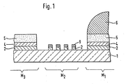
- Fig. 1 denotes an insulating substrate plate, for example made of soft glass or Al 2 O 3 ceramic or one with an insulation layer covered metal plate, for example made of spring steel or ferrite.
- a tantalum layer 2 containing the basic geometry of the circuit network is applied to the substrate plate 1.
- Layer 2 can also consist of tantalum nitride or tantalum oxynitride (TaO x N y ) or of a tantalum aluminum alloy. Instead of tantalum, it can also contain another valve metal, for example niobium, aluminum, zirconium or hafnium, as the main component.
- the tantalum layer 2 forms a first, a second and a third pattern of the electronic thin-film circuit, of which the first pattern M 1 defines a conductor track and / or a connection contact, the second pattern M 2 defines a temperature-independent resistance and the third pattern M 3 defines a temperature-dependent resistance .
- the tantalum layer 2 is covered with a boundary layer 4, which contains tantalum, tantalum oxide, nickel, nickel oxide and mixed phases of these components.
- a nickel layer 5 is arranged on the boundary layer 4 in the region of the first pattern M 1 and a solder layer 6 is arranged on the nickel layer 5, which solder layer may consist of lead-tin soft solder.
- the layers 2, 4, 5 and 6 form the conductor track and / or the connection contact in the region of the first pattern M 1 .
- the solder layer 6 can also be omitted or replaced by a galvanically applied reinforcing layer.
- the tantalum layer 2 forms the temperature-independent resistance and is covered with a tantalum oxide layer 9.
- the tantalum layer 2 is covered with the boundary layer 4 and the boundary layer 4 with the nickel layer 5, as in the region of the first pattern M 1 .
- Layers 2, 4 and 5 form in the area of third pattern M 3 the temperature-dependent resistance (sensor).
- the tantalum oxide layer 9 provided in the area of the second pattern M 2 can also be replaced by a layer 30 (compare FIGS. 2i and 3!), The formation and composition of which is described below.
- FIG. 2a to 2n show the electronic thin-film circuit according to FIG. 1, which is being produced, in the various process steps to be carried out according to the invention.
- the tantalum layer 2 is first applied to the insulating substrate plate 1 as a continuous layer by sputtering (FIG. 2a). Their layer thickness results from the two tasks that are assigned to this tantalum layer. It is an adhesion promoter between the substrate plate 1 and all subsequent layers.
- the second pattern M 2 long-term stable, anodically adjustable, largely temperature-independent resistors with a temperature coefficient of less than 100 ppm / o C h are produced , the relative change in resistance due to mechanical deformation being about twice as great as that caused thereby relative resistance extension.
- this tantalum adhesion and resistance layer 2 should have a sheet resistance which is between 20 and 200 ⁇ , preferably 50 ⁇ .
- the tantalum layer 2 is first oxidized to form the tantalum oxide layer 3 (FIG. 2b) on the exposed surface, preferably in a plate washing and drying process in which all foreign particles are removed from its surface at the same time, which lead to defects in the further layer structure can.
- the thickness of the tantalum oxide layer 3 is adjusted to 3 to 10 nm, preferably to 5 nm, with the aid of the temperature and duration of the plate drying. It is in any case thicker than the natural tantalum surface oxide layer, which slowly forms when the plates are stored.
- the oxide layer 3 can also be produced by other methods, for example with the aid of anodic oxidation, the desired thickness then being adjustable via the adjustment parameters.
- the tantalum layer 2 covered with the closed oxide layer 3 is covered over the entire area with a nickel layer 5, the sputtering energy being chosen so high that firstly the tantalum layer 2 is pre-aged as a result of the thermal load and thus maintains its long-term stability, and that it secondly, there is an intermetallic diffusion of nickel atoms into the tantalum oxide layer 3, a boundary layer 4 (FIG. 2c) containing tantalum, tantalum oxide, nickel, nickel oxide and mixed phases of these constituents being formed via reduction and oxidation processes and which excels the nickel layer 5 on the tantalum layer 2 anchored and produces a good ohmic contact between the tantalum layer 2 and the nickel layer 5.
- a boundary layer 4 FIG. 2c
- the necessary surface oxidation of the tantalum layer is produced in a delayed cooling phase by reaction with the residual oxidation gas. If, for other reasons, the energy of the nickel dusting has to be kept so low that the nickel diffusion into the tantalum oxide layer has not yet taken place sufficiently, the diffusion can process and the aging of the tantalum layer also take place in a subsequent tempering process.
- the nickel layer 5 in the area of the first pattern M 1 or in partial areas thereof can be the basis for galvanic amplification in order to also include active components, for example chip transistors, by means of bond connections (FIG. 3! Include thin layer circuit. So that the galvanic reinforcement runs well and is deposited with a uniform thickness on all areas of the nickel layer to be galvanically reinforced, the surface resistance of the nickel layer should be less than 5 ⁇ , preferably 0.5 ⁇ .
- the nickel layer 5 in the area of the first pattern M 1 (see FIG. 1 !) Or in partial areas of it (see FIG. 3! Can be a soldering partner for the lead-tin-soft solder layer 6 necessary to achieve sufficient good conductivity preferably over all conductor tracks, connection points and connection contacts extends, so is the main component of these areas M 1 itself. It is particularly important for the present invention that the thickness of the nickel layer 5 does not have to be adapted to the soldering process, but its thickness is optimized in accordance with the other two tasks, and nevertheless that the layer system has excellent soldering stability. This is due to the boundary layer 4 introduced according to the invention, which is only partially soluble in the lead-tin soft solder (FIG. 4d).
- the boundary layer 4 prevents the soft solder from contacting the tantalum layer 2 comes and contracts like a drop.
- the adhesion of the solder layer and the components and connection conductors soldered to it remains unchanged, so that even if the soft solder has penetrated to the boundary layer, the adhesion is limited by the breaking strength of the substrate material used or of the solder itself.
- the sputtering of the nickel layer 5 is preferably carried out with hydrogen doping of the discharge gas in order to increase the temperature coefficients of the nickel layer and because then the solder wetting unexpectedly proceeds so well that it can be soldered without protective gilding and without surface activation by etching or flux.
- the etching is carried out in a two-step process.
- the nickel layer 5 and the majority of the barrier layer 4 is in a mixture of 190 g / 1 (NH 4) 2 S 2 O 8 practical with 460 g / l H 2 S0 4 without Un - terfordung selectively etched from the tantalum layer 2 under the lacquer edge, a small part 30 (FIG. 2e) of the boundary layer 4 remaining.
- the rest 30 of the boundary layer 4 and the tantalum layer 2 are mixed with 190 g / l (NH 4 ) 2 S 2 O 8 with 125 g / 1 HF, which nickel is practically not attacks, etched off.
- the nickel layer 5 is thus an etching mask for the tantalum layer 2, whereby the Tantalunterfordung based on the coating edge to 1 / is to be limited.
- the nickel etching under the lacquer edge is practically negligible even in the event of long overetching in order to reliably expose the tantalum resistance surfaces. Even with etching time, which is ten times as long as normal etching time, the undercutting remains at 4 / to be limited. After the surface has been etched free, a nickel passivation layer unexpectedly forms on the nickel-lacquer etching edge, which prevents under-etching.
- an adjustment mask 91 (FIG. 2k) has to be produced beforehand. The procedure is as follows:
- the surface must be water-free before the second coating of lacquer, otherwise lacquer adhesion problems occur.
- the etched plates are dried in the oven at at least 120 ° C. for about 30 ', which due to the corrosion stability of the nickel layer 5 has no consequences for the solder wettability and guarantees excellent paint adhesion even on the exposed substrate surfaces.
- the adjustment mask 91 is then produced by coating, exposure and development, the coating thickness resulting from the required dielectric strength.
- an electrolyte and an adjustment method of this type must be selected for the anodic oxidation so that this layer, which still contains nickel oxides, is dissolved as quickly as possible in the electrolyte and does not interfere with the adjustment process.
- electrolytes containing Na 2 SO 4 and / or NH 4 Cl if first a constant voltage between 1 and 10 volts is applied to all resistors, which is above the solution potentials of nickel and of oxidic Ta-Ni mixed phase-n lies in the selected electrolyte. For 0.5 m Na 2 SO 4 , this voltage is preferably 3 volts.
- the solution process is completed particularly quickly when the generator used has a high current limit tion has so that the charge required for the dissolution process can flow freely. At the same time, all the remaining nickel layer residues are then replaced by the resistance tracks, which are left as etching residues in selective nickel etching, for example due to paint mask defects.
- a high adjustment current should first be chosen to shorten the resolution process until a noticeable R adjustment takes place, for example up to 10% R increase. The rest of the adjustment must then be carried out with such a low current density that after the adjustment all resistances of the circuit lie within the required tolerance limit, the R-stroke being able to be selected specifically for the circuit by means of high current.
- the tantalum layer 2 is covered with a tantalum oxide layer 9 in the area of the second pattern M 2 (FIG. 21).
- the matching mask 91 is now detached (FIG. 2m) and then a mask 92 made of solder resist is applied to the nickel layer 5 in the region of the third pattern M 3 (FIG. 2n).
- the system 1, 2, 4, 5, 9, 92 shown in Fig. 2n is now immersed in liquid lead-tin soft solder.
- the liquid solder does not wet the resistance tracks 2 with the valve metal oxide layer 9 in the area of the second pattern M 2 and the resistance tracks 2, 4, 5 covered with the mask 92 in the area of the third pattern M 3.
- Those in the area of the first pattern M 1 The exposed upper side of the metallization 2, 4, 5, on the other hand, is replaced by the liquid solder to form a solder layer 6 wetted so that after detaching the solder mask 92 the structure shown in Fig. 1 is formed, which represents the finished electronic thin-film circuit.
- the solder layer 6 the electrical conductivity of the conductor tracks and connection contacts is considerably increased.
- FIG. 3 shows a thin-film hybrid as an application example of an electronic thin-film circuit according to the invention.
- the substrate plate is again designated 1, the tantalum layer 2.
- 9 denotes an oxide layer formed by anodic oxidation on a balanced tantalum resistor 11.
- a conductor track area reinforced with a lead-tin soft solder layer is shown at 10.
- a galvanically reinforced conductor track part with bond contact 16 is shown at 12.
- a component soldered in the reflow process is designated.
- An unbalanced tantalum resistor with protective layer 30 is shown at 14. With 15 a temperature-h teiliger resistor (sensor) is indicated, with 17 an imprinted CP-resistance (conductive plastic resistor).
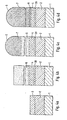
- FIGS. 4a to 4d show the formation of the boundary layer 4 and its effect as a solder barrier layer.
- 4a shows the layer system 2, 3 after the formation of the tantalum oxide layer 3.
- FIG. 4b shows the same layer system after the additional application of the nickel layer 5. It can be seen how the boundary layer 4 has been formed from the oxide layer 3.
- 30 denotes that part of the boundary layer 4 which does not dissolve in the selective nickel etchant and which serves as a protective layer in the case of the non-matching tantalum resistor (compare position 14 in FIG. 3!).
- Figures 4c and 4d show the same layer system as in Fig. 4b, however after the application of the lead-tin soft solder layer 6.
- FIG. 1 shows the layer system 2, 3 after the formation of the tantalum oxide layer 3.
- FIG. 4b shows the same layer system after the additional application of the nickel layer 5. It can be seen how the boundary layer 4 has been formed from the oxide layer 3.
- 30 denotes that part of the boundary layer 4 which does
- FIG. 4c shows this system with a short soldering time and / or low soldering temperature, FIG. 4d with a long soldering time and / or high soldering temperature.
- FIG. 4c only a part of the nickel layer 5 has dissolved in the solder 6, in FIG. 4d the entire nickel layer 5. Furthermore, a part 8 of the boundary layer 4 has still been detached from the solder there.
- 7 denotes the part of the nickel layer dissolved in solder 6.
Landscapes
- Apparatuses And Processes For Manufacturing Resistors (AREA)
- Parts Printed On Printed Circuit Boards (AREA)
- Non-Adjustable Resistors (AREA)
- Manufacturing Of Printed Circuit Boards (AREA)
- Manufacturing Of Printed Wiring (AREA)
Applications Claiming Priority (2)
| Application Number | Priority Date | Filing Date | Title |
|---|---|---|---|
| DE2906813 | 1979-02-22 | ||
| DE2906813A DE2906813C2 (de) | 1979-02-22 | 1979-02-22 | Elektronische Dünnschichtschaltung |
Publications (2)
| Publication Number | Publication Date |
|---|---|
| EP0016251A1 true EP0016251A1 (fr) | 1980-10-01 |
| EP0016251B1 EP0016251B1 (fr) | 1982-06-16 |
Family
ID=6063581
Family Applications (1)
| Application Number | Title | Priority Date | Filing Date |
|---|---|---|---|
| EP79104498A Expired EP0016251B1 (fr) | 1979-02-22 | 1979-11-14 | Circuit électronique à film mince et procédé pour sa fabrication |
Country Status (4)
| Country | Link |
|---|---|
| US (1) | US4358748A (fr) |
| EP (1) | EP0016251B1 (fr) |
| JP (1) | JPS55146902A (fr) |
| DE (2) | DE2906813C2 (fr) |
Cited By (3)
| Publication number | Priority date | Publication date | Assignee | Title |
|---|---|---|---|---|
| WO1982003458A1 (fr) * | 1981-04-04 | 1982-10-14 | Burger Kurt | Jauge de contrainte a couche mince et procede pour sa fabrication |
| WO1983001344A1 (fr) * | 1981-10-06 | 1983-04-14 | Gruner, Heiko | Circuit electronique a couche mince et son procede de fabrication |
| EP0380122A1 (fr) * | 1989-01-26 | 1990-08-01 | Casio Computer Company Limited | Mémoire à couche mince et procédé pour sa fabrication |
Families Citing this family (15)
| Publication number | Priority date | Publication date | Assignee | Title |
|---|---|---|---|---|
| DE3024297C2 (de) * | 1980-06-27 | 1985-08-14 | Endress U. Hauser Gmbh U. Co, 7867 Maulburg | Kapazitiver Feuchtigkeitsfühler und Verfahren zum Herstellen seiner feuchtigkeitsempfindlichen Schicht |
| DE3136198A1 (de) * | 1981-01-15 | 1982-08-05 | Robert Bosch Gmbh, 7000 Stuttgart | "elektronische duennschichtschaltung" |
| DE3151630C2 (de) * | 1981-12-28 | 1986-07-03 | Endress U. Hauser Gmbh U. Co, 7867 Maulburg | Feuchtigkeitsfühler und Verfahren zu seiner Herstellung |
| JPS59185801U (ja) * | 1983-05-26 | 1984-12-10 | アルプス電気株式会社 | チツプ抵抗 |
| US4847445A (en) * | 1985-02-01 | 1989-07-11 | Tektronix, Inc. | Zirconium thin-film metal conductor systems |
| DE3604368A1 (de) * | 1985-02-13 | 1986-08-14 | Sharp K.K., Osaka | Verfahren zur herstellung eines duennfilm-transistors |
| DE3605425A1 (de) * | 1986-02-20 | 1987-08-27 | Standard Elektrik Lorenz Ag | Duennschichtschaltung und ein verfahren zu ihrer herstellung |
| US4719443A (en) * | 1986-04-03 | 1988-01-12 | General Electric Company | Low capacitance power resistor using beryllia dielectric heat sink layer and low toxicity method for its manufacture |
| US4829553A (en) * | 1988-01-19 | 1989-05-09 | Matsushita Electric Industrial Co., Ltd. | Chip type component |
| DE3829195A1 (de) * | 1988-08-29 | 1990-03-08 | Bosch Gmbh Robert | Temperaturfuehler |
| US5591480A (en) * | 1995-08-21 | 1997-01-07 | Motorola, Inc. | Method for fabricating metallization patterns on an electronic substrate |
| US6933186B2 (en) * | 2001-09-21 | 2005-08-23 | International Business Machines Corporation | Method for BEOL resistor tolerance improvement using anodic oxidation |
| JP4811756B2 (ja) * | 2001-09-28 | 2011-11-09 | Dowaメタルテック株式会社 | 金属−セラミックス接合回路基板の製造方法 |
| US7771604B2 (en) * | 2004-10-04 | 2010-08-10 | International Business Machines Corporation | Reduced mask count gate conductor definition |
| DE102005053930B4 (de) * | 2005-11-11 | 2014-10-30 | Rohde & Schwarz Gmbh & Co. Kg | Befestigungs- und Kontaktvorrichtung für ein Substrat |
Citations (8)
| Publication number | Priority date | Publication date | Assignee | Title |
|---|---|---|---|---|
| US3487522A (en) * | 1966-02-01 | 1970-01-06 | Western Electric Co | Multilayered thin-film intermediates employing parting layers to permit selective,sequential etching |
| DE1665571B1 (de) * | 1966-03-08 | 1971-09-09 | Siemens Ag | Verfahren zur herstellung von duennschichtbaugruppen der elektronik |
| DE2157923A1 (de) * | 1970-11-27 | 1972-06-08 | Western Electric Co | Verfahren zur Herstellung einer bestimmten RC Schaltung |
| DE2105411B2 (de) * | 1970-02-10 | 1972-12-28 | Fujitsu Ltd., Kawasaki, Kanagawa (Japan) | Verfahren zum herstellen von integrierten duennfilmschaltungen |
| US3949275A (en) * | 1973-06-20 | 1976-04-06 | Siemens Aktiengesellschaft | Electric thin-film circuit and method for its production |
| DE2509912A1 (de) * | 1975-03-07 | 1976-09-16 | Bosch Gmbh Robert | Elektronische duennfilmschaltung |
| DE2606086B2 (de) * | 1976-02-16 | 1978-11-30 | Bernd Dipl.-Ing. 7250 Leonberg Kaiser | Herstellung von integrierten Dünnschichtschaltungen aus mit dünnen Schichten mehrlagig beschichteter Unterlage |
| DE2746225A1 (de) * | 1977-09-14 | 1979-03-22 | Bbc Brown Boveri & Cie | Verfahren zur herstellung von lokalen anodischen oxidschichten |
Family Cites Families (7)
| Publication number | Priority date | Publication date | Assignee | Title |
|---|---|---|---|---|
| US3256588A (en) * | 1962-10-23 | 1966-06-21 | Philco Corp | Method of fabricating thin film r-c circuits on single substrate |
| US3544287A (en) * | 1967-04-13 | 1970-12-01 | Western Electric Co | Heat treatment of multilayered thin film structures employing oxide parting layers |
| US3621442A (en) * | 1968-11-07 | 1971-11-16 | Allen Bradley Co | Terminal connection of electronic devices |
| DE2522944C3 (de) * | 1975-05-23 | 1980-11-27 | Siemens Ag, 1000 Berlin Und 8000 Muenchen | Verfahren zur Herstellung einer elektrischen Dünnfilmschaltung |
| DE2657949A1 (de) * | 1975-10-17 | 1978-06-22 | Siemens Ag | Verfahren zum herstellen einer duennschichtschaltung |
| US4107632A (en) * | 1976-08-09 | 1978-08-15 | Texscan Corporation | Attenuator element |
| US4199745A (en) * | 1977-12-15 | 1980-04-22 | Trx, Inc. | Discrete electrical components |
-
1979
- 1979-02-22 DE DE2906813A patent/DE2906813C2/de not_active Expired
- 1979-11-14 EP EP79104498A patent/EP0016251B1/fr not_active Expired
- 1979-11-14 DE DE7979104498T patent/DE2963126D1/de not_active Expired
-
1980
- 1980-02-01 US US06/117,452 patent/US4358748A/en not_active Expired - Lifetime
- 1980-02-22 JP JP2070380A patent/JPS55146902A/ja active Granted
Patent Citations (11)
| Publication number | Priority date | Publication date | Assignee | Title |
|---|---|---|---|---|
| US3487522A (en) * | 1966-02-01 | 1970-01-06 | Western Electric Co | Multilayered thin-film intermediates employing parting layers to permit selective,sequential etching |
| DE1665571B1 (de) * | 1966-03-08 | 1971-09-09 | Siemens Ag | Verfahren zur herstellung von duennschichtbaugruppen der elektronik |
| DE2105411B2 (de) * | 1970-02-10 | 1972-12-28 | Fujitsu Ltd., Kawasaki, Kanagawa (Japan) | Verfahren zum herstellen von integrierten duennfilmschaltungen |
| DE2157923A1 (de) * | 1970-11-27 | 1972-06-08 | Western Electric Co | Verfahren zur Herstellung einer bestimmten RC Schaltung |
| US3718565A (en) * | 1970-11-27 | 1973-02-27 | Bell Telephone Labor Inc | Technique for the fabrication of discrete rc structure |
| US3949275A (en) * | 1973-06-20 | 1976-04-06 | Siemens Aktiengesellschaft | Electric thin-film circuit and method for its production |
| DE2331586B2 (de) * | 1973-06-20 | 1976-11-25 | Siemens AG, 1000 Berlin und 8000 München | Aluminium-tantal-schichten fuer duennschichtschaltungen sowie diskrete widerstaende und kondensatoren |
| DE2509912A1 (de) * | 1975-03-07 | 1976-09-16 | Bosch Gmbh Robert | Elektronische duennfilmschaltung |
| US4075416A (en) * | 1975-03-07 | 1978-02-21 | Robert Bosch Gmbh | Electronic thin film circuit unit and method of making the same |
| DE2606086B2 (de) * | 1976-02-16 | 1978-11-30 | Bernd Dipl.-Ing. 7250 Leonberg Kaiser | Herstellung von integrierten Dünnschichtschaltungen aus mit dünnen Schichten mehrlagig beschichteter Unterlage |
| DE2746225A1 (de) * | 1977-09-14 | 1979-03-22 | Bbc Brown Boveri & Cie | Verfahren zur herstellung von lokalen anodischen oxidschichten |
Cited By (4)
| Publication number | Priority date | Publication date | Assignee | Title |
|---|---|---|---|---|
| WO1982003458A1 (fr) * | 1981-04-04 | 1982-10-14 | Burger Kurt | Jauge de contrainte a couche mince et procede pour sa fabrication |
| US4620365A (en) * | 1981-04-04 | 1986-11-04 | Robert Bosch Gmbh | Method of making a thin-film strain gauge |
| WO1983001344A1 (fr) * | 1981-10-06 | 1983-04-14 | Gruner, Heiko | Circuit electronique a couche mince et son procede de fabrication |
| EP0380122A1 (fr) * | 1989-01-26 | 1990-08-01 | Casio Computer Company Limited | Mémoire à couche mince et procédé pour sa fabrication |
Also Published As
| Publication number | Publication date |
|---|---|
| JPS55146902A (en) | 1980-11-15 |
| EP0016251B1 (fr) | 1982-06-16 |
| DE2906813A1 (de) | 1980-09-04 |
| DE2963126D1 (en) | 1982-08-05 |
| US4358748A (en) | 1982-11-09 |
| DE2906813C2 (de) | 1982-06-03 |
| JPS6255706B2 (fr) | 1987-11-20 |
Similar Documents
| Publication | Publication Date | Title |
|---|---|---|
| EP0016251B1 (fr) | Circuit électronique à film mince et procédé pour sa fabrication | |
| DE2729030C2 (de) | Verfahren zum Herstellen eines mehrschichtigen Leiterzugsmusters für monolithisch integrierte Halbleiterschaltungen | |
| DE69005785T2 (de) | Elektrischer Widerstand in Chip-Bauweise für Oberflächenbestückung und Verfahren zu seiner Herstellung. | |
| DE3340563C2 (de) | Schichtkondensator und Verfahren zur Herstellung desselben | |
| DE2554691C2 (de) | Verfahren zum Herstellen elektrischer Leiter auf einem isolierenden Substrat und danach hergestellte Dünnschichtschaltung | |
| DE2901697C3 (de) | Verfahren zur Ausbildung von Leitungsverbindungen auf einem Substrat | |
| DE2509912C3 (de) | Elektronische Dünnfilmschaltung | |
| DE2709933A1 (de) | Verfahren zum herstellen durchgehender metallischer verbindungen zwischen mehreren metallisierungsebenen in halbleitervorrichtungen | |
| DE2024494A1 (de) | Verfahren zur Beseitigung von durch Fehlstellen, insbesondere Nadellöcher verursachten Kurzschlüssen in DünnschichtÜberkreuzungen | |
| DE3123213A1 (de) | Hybridschaltung mit integrierten kondensatoren und widerstaenden und verfahren zu ihrer herstellung | |
| DE2315710A1 (de) | Verfahren zum herstellen einer halbleiteranordnung | |
| DE10039710B4 (de) | Verfahren zur Herstellung passiver Bauelemente auf einem Halbleitersubstrat | |
| EP0013728B1 (fr) | Procédé pour former des connexions électriques entre des couches conductrices dans des structures semi-conductrices | |
| DE3605425A1 (de) | Duennschichtschaltung und ein verfahren zu ihrer herstellung | |
| DE2926516A1 (de) | Verfahren zur herstellung eines metallfolienwiderstandes und metallfolienwiderstand | |
| DE2539193B2 (de) | Verfahren zur herstellung eines planaren leiterbahnsystems fuer integrierte halbleiterschaltungen | |
| EP0016263A1 (fr) | Résistance en couche mince à coefficient de température élevé et procédé pour sa fabrication | |
| DE19501693C2 (de) | Verfahren zum Herstellen von elektronischen Bauelementen und mit diesem Verfahren hergestelltes elektronisches Bauelement | |
| DE102008016613B4 (de) | Verfahren zur Herstellung eines elektrischen Bauelements mit mindestens einer dielektrischen Schicht und ein elektrisches Bauelement mit mindestens einer dielektrischen Schicht | |
| DE1614786C3 (de) | Halbleiteranordnung mit mehrschichtigen Leiterbahnen und Verfahren zum Herstellen dieser Halbleiteranordnung | |
| DE2331586C3 (de) | Aluminium-Tantal-Schichten für Dünnschichtschaltungen sowie diskrete Widerstände und Kondensatoren | |
| DE2653814C3 (de) | Verfahren zur Herstellung einer elektrischen Dünnschichtschaltung | |
| DE1665571B1 (de) | Verfahren zur herstellung von duennschichtbaugruppen der elektronik | |
| DE2114118A1 (de) | Gedruckte Schaltung und Verfahren zu ihrer Herstellung | |
| DE1540175C (de) | Verfahren zur Herstellung von Kon takten |
Legal Events
| Date | Code | Title | Description |
|---|---|---|---|
| PUAI | Public reference made under article 153(3) epc to a published international application that has entered the european phase |
Free format text: ORIGINAL CODE: 0009012 |
|
| 17P | Request for examination filed | ||
| AK | Designated contracting states |
Designated state(s): CH DE FR GB IT NL |
|
| ITF | It: translation for a ep patent filed | ||
| GRAA | (expected) grant |
Free format text: ORIGINAL CODE: 0009210 |
|
| AK | Designated contracting states |
Designated state(s): CH DE FR GB IT NL |
|
| REF | Corresponds to: |
Ref document number: 2963126 Country of ref document: DE Date of ref document: 19820805 |
|
| REG | Reference to a national code |
Ref country code: FR Ref legal event code: DL |
|
| REG | Reference to a national code |
Ref country code: GB Ref legal event code: 746 |
|
| ITPR | It: changes in ownership of a european patent |
Owner name: OFFERTA DI LICENZA AL PUBBLICO |
|
| PGFP | Annual fee paid to national office [announced via postgrant information from national office to epo] |
Ref country code: GB Payment date: 19900905 Year of fee payment: 12 |
|
| PGFP | Annual fee paid to national office [announced via postgrant information from national office to epo] |
Ref country code: FR Payment date: 19901129 Year of fee payment: 12 |
|
| ITTA | It: last paid annual fee | ||
| PGFP | Annual fee paid to national office [announced via postgrant information from national office to epo] |
Ref country code: NL Payment date: 19901130 Year of fee payment: 12 |
|
| PGFP | Annual fee paid to national office [announced via postgrant information from national office to epo] |
Ref country code: CH Payment date: 19910221 Year of fee payment: 12 |
|
| PG25 | Lapsed in a contracting state [announced via postgrant information from national office to epo] |
Ref country code: GB Effective date: 19911114 |
|
| PG25 | Lapsed in a contracting state [announced via postgrant information from national office to epo] |
Ref country code: CH Effective date: 19911130 |
|
| PGFP | Annual fee paid to national office [announced via postgrant information from national office to epo] |
Ref country code: DE Payment date: 19920129 Year of fee payment: 13 |
|
| PG25 | Lapsed in a contracting state [announced via postgrant information from national office to epo] |
Ref country code: NL Effective date: 19920601 |
|
| GBPC | Gb: european patent ceased through non-payment of renewal fee | ||
| NLV4 | Nl: lapsed or anulled due to non-payment of the annual fee | ||
| PG25 | Lapsed in a contracting state [announced via postgrant information from national office to epo] |
Ref country code: FR Effective date: 19920731 |
|
| REG | Reference to a national code |
Ref country code: CH Ref legal event code: PL |
|
| REG | Reference to a national code |
Ref country code: FR Ref legal event code: ST |
|
| PG25 | Lapsed in a contracting state [announced via postgrant information from national office to epo] |
Ref country code: DE Effective date: 19930803 |
|
| PLBE | No opposition filed within time limit |
Free format text: ORIGINAL CODE: 0009261 |
|
| STAA | Information on the status of an ep patent application or granted ep patent |
Free format text: STATUS: NO OPPOSITION FILED WITHIN TIME LIMIT |