EP0016603A1 - Verfahren zur Behandlung von Substraten durch Plasma - Google Patents
Verfahren zur Behandlung von Substraten durch Plasma Download PDFInfo
- Publication number
- EP0016603A1 EP0016603A1 EP80300752A EP80300752A EP0016603A1 EP 0016603 A1 EP0016603 A1 EP 0016603A1 EP 80300752 A EP80300752 A EP 80300752A EP 80300752 A EP80300752 A EP 80300752A EP 0016603 A1 EP0016603 A1 EP 0016603A1
- Authority
- EP
- European Patent Office
- Prior art keywords
- electrode plates
- bus lines
- plasma
- substrate materials
- pair
- Prior art date
- Legal status (The legal status is an assumption and is not a legal conclusion. Google has not performed a legal analysis and makes no representation as to the accuracy of the status listed.)
- Granted
Links
Images


Classifications
-
- H—ELECTRICITY
- H01—ELECTRIC ELEMENTS
- H01J—ELECTRIC DISCHARGE TUBES OR DISCHARGE LAMPS
- H01J37/00—Discharge tubes with provision for introducing objects or material to be exposed to the discharge, e.g. for the purpose of examination or processing thereof
- H01J37/32—Gas-filled discharge tubes
- H01J37/32009—Arrangements for generation of plasma specially adapted for examination or treatment of objects, e.g. plasma sources
- H01J37/32082—Radio frequency generated discharge
-
- C—CHEMISTRY; METALLURGY
- C23—COATING METALLIC MATERIAL; COATING MATERIAL WITH METALLIC MATERIAL; CHEMICAL SURFACE TREATMENT; DIFFUSION TREATMENT OF METALLIC MATERIAL; COATING BY VACUUM EVAPORATION, BY SPUTTERING, BY ION IMPLANTATION OR BY CHEMICAL VAPOUR DEPOSITION, IN GENERAL; INHIBITING CORROSION OF METALLIC MATERIAL OR INCRUSTATION IN GENERAL
- C23C—COATING METALLIC MATERIAL; COATING MATERIAL WITH METALLIC MATERIAL; SURFACE TREATMENT OF METALLIC MATERIAL BY DIFFUSION INTO THE SURFACE, BY CHEMICAL CONVERSION OR SUBSTITUTION; COATING BY VACUUM EVAPORATION, BY SPUTTERING, BY ION IMPLANTATION OR BY CHEMICAL VAPOUR DEPOSITION, IN GENERAL
- C23C16/00—Chemical coating by decomposition of gaseous compounds, without leaving reaction products of surface material in the coating, i.e. chemical vapour deposition [CVD] processes
- C23C16/44—Chemical coating by decomposition of gaseous compounds, without leaving reaction products of surface material in the coating, i.e. chemical vapour deposition [CVD] processes characterised by the method of coating
- C23C16/50—Chemical coating by decomposition of gaseous compounds, without leaving reaction products of surface material in the coating, i.e. chemical vapour deposition [CVD] processes characterised by the method of coating using electric discharges
- C23C16/505—Chemical coating by decomposition of gaseous compounds, without leaving reaction products of surface material in the coating, i.e. chemical vapour deposition [CVD] processes characterised by the method of coating using electric discharges using radio frequency discharges
- C23C16/509—Chemical coating by decomposition of gaseous compounds, without leaving reaction products of surface material in the coating, i.e. chemical vapour deposition [CVD] processes characterised by the method of coating using electric discharges using radio frequency discharges using internal electrodes
-
- H—ELECTRICITY
- H10—SEMICONDUCTOR DEVICES; ELECTRIC SOLID-STATE DEVICES NOT OTHERWISE PROVIDED FOR
- H10P—GENERIC PROCESSES OR APPARATUS FOR THE MANUFACTURE OR TREATMENT OF DEVICES COVERED BY CLASS H10
- H10P14/00—Formation of materials, e.g. in the shape of layers or pillars
- H10P14/60—Formation of materials, e.g. in the shape of layers or pillars of insulating materials
Definitions
- the present invention relates to a method for processing substrate materials by means of treating plasma and more particularly to a method for processing semiconductor wafers by means of treating plasma, such as by a chemical vapor deposition (CVD) or by an etching process.
- CVD chemical vapor deposition
- the reaction gas consists of, for example, monosilane (SiH 4 ) and nitrous oxide (N 2 0) or ammonia (NH 3 ).
- the reaction gas consists of, for example,tetrachlorocarbon (CC1 4 ) or tetrafluoride (CF 4 ).
- silicon dioxide (Si0 2 ) or silicon nitride (Si 3 N 4 ) is produced and deposited on the wafers by means of the plasma to form an insulating film on each wafer.
- the insulating films of silicon dioxide or silicon nitride are etched away by means of the plasma and, particularly, by means of the radicals in the plasma.
- polycrystalline silicon or metal oxide such as aluminum oxide can be coated on the surfaces of the wafers by means of decomposition of monosilane (SiH 4 ).
- silicon wafers constituting substrate materials can be etched away by means of tetrafluoride (CF4)' or metal layers such as aluminum (Al) or molybdenum (Mo) can be etched away by means of tetrachloro-carbon (CC1 4 ).
- CF4' tetrafluoride
- metal layers such as aluminum (Al) or molybdenum (Mo) can be etched away by means of tetrachloro-carbon (CC1 4 ).
- the present invention intends to solve the above-mentioned problems in the prior art.
- a method for processing substrate materials by treating plasma including the steps of mounting said substrate materials onto a series of electrode plates arranged in parallel to each other, alternately connecting said electrode plates to a pair of bus lines, and applying a high-frequency power between said pair of bus lines for producing plasma between said electrode plates, said method comprising the step of changing the feeding points of said high-frequency power on said pair of bus lines so that said plasma treatment is effected substantially uniformly in the spaces between said electrode plates.
- FIG. 10a through 10c illustrates two graphs substantially showing the distribution of the electric field intensities when the feeding points of the power to the bus lines are changed according to the present invention
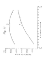
- Fig. 11 illustrates a result of an experiment according to one embodiment of the present invention
- Fig. 12 is a schematic circuit diagram of an electrode structure for explaining the method of applying high-frequency voltage to the electrode plates according to one embodiment of the present invention
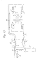
- Fig. 13 is a schematic diagram showing a switching mechanism for applying high-frequency power to the electrode structure of Fig. 12, and
- Fig. 14 is another embodiment of a schematic circuit diagram of an electrode structure, according to the present invention.
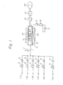
- Fig. 1 is a schematic diagram illustrating a plasma treatment apparatus for explaining the fundamental method of the prior art.
- a reaction gas of nitrous oxide (N 2 O), nitrogen (N 2 ), monosilane (SiH 4 ), ammonia ( NH 3) or tetrafluoride ( CF 4) is introduced from gas inlets 1(1), 1(2), 1(3), 1(4) or 1(5) respectively through a needle valve 3, a stop valve 5 and a duct 7 into a reaction tube 9 made of quartz.
- the amount of the introduced gas is controlled by each needle valve 3.
- a number of electrode plates 13 are arranged in parallel to each other and are perpendicular to the longitudinal direction of the reaction tube 9.
- a semiconductor wafer 15 is mounted on a surface of each electrode plate 13.
- a high-frequency voltage is applied from a high-frequency oscillator (power supply) 17 through a power amplifier 19 and a control unit 21 including a power coupler (not shown) to the electrode plates 13 in such a manner as herein after described.
- a heating furnace 23 is electrically conducted to heat the quartz tube 9.
- a plasma is produced within the quartz tube 9.
- monosilane (SiH 4 J and ammonia (NH 3 ) have been introduced into the quartz tube 9 for the purpose of a CVD process, the produced plasma causes the chemical reaction represented as:
- the silicon nitride (Si 3 N 4 ) produced by this reaction is then deposited on the wafers 15.
- the hydrogen (H 2 ) and by-product gas produced by that reaction is introduced into a cooling trap 25 by opening a stop valve 27.
- the low boiling point gas is exhausted by an exhaust pump 29.
- the valve 11 is used for replacing the gas within the quartz tube 9 by a desired gas.
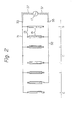
- Fig. 2 is a schematic diagram of the electrode portion within the quartz tube 9 of Fig. 1.
- each of the electrode plates 13 is electrically connected to the high-frequency power supply 17 through either bus line 31 or 32, in such a manner that each of the adjacent electrode plates 13 is connected to the opposite terminal of the power supply 17.
- the portion between the end point 33 of the bus line 31 and the power supply 17 and the portion between the end point 35 of the bus line 32 are connected by coaxial cables 37.
- the power amplifier 19 and the control unit 21 (Fig. 1) are not shown in Fig. 2, but they are -actually connected between the bus lines 31, 32 and the power supply 17.
- the feeding points of the high-frequency power supply 17 to the bus lines 31 and 32 are fixed to the end points 33 and 35, respectively.
- the positions of the electrode plates with respect to the longitudinal direction of the quartz tube 9 are scaled below the schematic diagram of Fig. 2 with symbols S, C and E which respectively represent the start position, the center position and the end position of the electrode plates with respect to the feeding terminals 33 and 35.
- Fig. 3 illustrates the deposition rates of the films on the wafers with respect to the positions of the electrode plates, for various frequencies applied to the electrode plates. As shown in Fig. 3, the higher the frequency of the applied power (3.5 MHz, 7 MH z, 13.56 MHz, 20 MHz), the more uneven the deposition rate becomes with rrespect to the positions of the electrode plates.
- Fig. 3 may also be adapted to explain the etching rates of the wafers by replacing the ordinate by "ETCHING RATE". The reason why the deposition rates or the etching rates are different will be described in conjunction with Figs. 4 through 9.
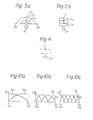
- Fig. 4(a) is an equivalent circuit diagram of F ig. 2.
- each of the inductance L 1 , L 2 ,..., L n-1 connected in series represents the bus line 31 between alternate electrode plates.
- Each of the inductance L 2 , L 4 ,..., L n connected in series represents the bus line 32 between alternate electrode plates.
- Each of the parallel circuits of C 1 and R 1 , of C 2 and R 2 ,..., and of C and R connected between the bus lines 31 and 32 n n represents a pair of adjacent electrode plates.
- Figs. 5a and b there are provided equivalent circuits of a well known dipole antenna.
- the capacitors C l , C 2 ,..., C n represent distributed capacitances on a dipole antenna 39.
- the circuit of Fig. 5a can be drawn as an equivalent circuit, as illustrated in Fig. 5b.
- circuit of Fig. 4b which is an equivalent circuit of the electrode structure of Fig. 2
- circuit of Fig. 5b which is an equivalent circuit of the dipole antenna of Fig. 5a
- Fig. 6 the circuit of Fig. 6b
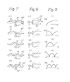
- F ig. 7(1) illustrates a current distribution curve 41 and a voltage distribution curve 43' on a dipole antenna when a half wave length of a power is fed from a power supply 17' to the two elements 45 and 46 of the dipole antenna.
- Figs. 7(2) through 7(5) also show these curves 41 and 43' on the dipole antenna when receiving ⁇ , 3/2X, 2 ⁇ , and 5/2 respectively, where the notation ⁇ represents one wave length of the power fed from the power supply 17'.
- the current distributions show zero at both ends E of the antenna elements 45, 46, and show maximum at the feeding points S.
- the voltage distributions show maximum at both ends E of the antenna elements and zero at the feeding points S.
- the only difference among Figs. 7(1) through 7(5) is that, when the wave length of the power fed to the antenna becomes short, accordingly the number of the standing waves of current or voltage is increased.
- Fig. 9(1) is a graph of a distribution of the intensity of the electric field in the reaction tube 9 of Fig. 1.
- the abscissa represents the position of the electrode plates in the longitudinal direction of the reaction tube 9 from the feeding point S to the end point E
- the ordinate represents the absolute value of the intensity of the electric field in the reaction tube 9.
- This graph can easily be obtained from the voltage distribution of Fig. 8(1).
- Fig. 8(1) since the polarities of the voltages on the bus lines 31 and 32 are opposite to each other, the potential difference between the bus lines 31 and 32 is maximum at the end point E of the reaction tube 9.
- the absolute value of the electric field intensity is maximum at the end point E of the reaction tube.
- Figs. 9(2) through 9(5) also show graphs of electric field intensities in the reaction tube and correspond to Figs. 8(2) through 8(5), respectively.
- the electric-field intensity varies with respect to the position in the reaction tube. It is well known that the thickness of a film formed by a plasma CVD process is nearly proportional to the intensity of the electic field. Therefore, the variations of the electric-field intensity, as illustrated in Figs. 9(1) through 9(5), result in non-uniform thickness of films on the wafers with respect to their positions in the reaction tube. Also, for the same reason, the depth of the plasma etching cannot be uniform with respect to the positions of the wafers.
- the present invention intends to improve the uniformness of the thickness of the films deposited on the wafers by the plasma CVD process or portions etched away from the wafers by the plasma etching process.
- Fig. 10a illustrates two lines showing electric field intensities when the feeding points of the power to the bus lines are changed according to the present invention.
- the curve 52 is the same as the curve of Fig. 9a. If the feeding point S 1 and the end point E 1 in the reaction tube are exchanged so that the new feeding point S 2 corresponds to the original end point E 1 and the new end point E 2 corresponds to the original feeding point S 1 , the reversed curve 54 will be obtained.
- the feeding point is fixed to the point S 1 during the first half period of a plasma CVD process, and then during the last half period of the process, the feeding point is fixed to the point S 2'
- the thickness of the films deposited on the wafers become almost uniform regardless of the electrode positions from the feeding point S 1 to the end point E 1 .
- Fig. 10b and Fig. 10c correspond to Fig. 9(3) and Fig. 9(5), respectively.
- the curve 54 can be obtained by exchaning the feeding points, as in the case of Fig. 10a.
- Fig. 11 illustrates a result of an experiment according to one embodiment of the present invention. The experiment was performed under the following conditions:
- Fig. 12 is a schematic circuit diagram of an electrode structure for explaining the method of applying high-frequency voltage to the electrode plates, according to one embodiment of the present invention.
- one terminal of the high-frequency power supply 17 is connected through a switch SW 1 to a right end point 33a of a bus line 31a or a right end point 33b of a bus line 31b, and, the other terminal of the power supply 17 is connected through a switch SW 2 to a right end point 35a of a bus line 32a or a right end point 35b of a bus line 32b.
- the bus line 31a is connected to the bus line 31b at the left-most point 33c of the bus line 31a.
- the bus line 32a is connected to the bus line 32b at the left-most point 35c of the bus line 32a.
- the power supply 17 is connected between the end points 33a and 35a.
- the situation of the electrode structure is the same as that of Fig. 2 and thus, after this period, the film deposited on the right-most wafer 15(1), which is nearest to the feeding point 35a, is thinnest and the film deposited on the left-most wafer 15(16), which is the farthest from the feeding point 33a, is thickest.
- the switches SW and S69 2 are switched so that the power supply 17 is connected between the end point 33b of the bus line 31b and the end point 35b of the bus line 32b and then the last half period of the processing is executed.
- the feeding point from one terminal of the power supply is the point 33c and the other feeding point is 35c. Therefore, after this last half period, substantially uniform thicknesses of films can be obtained.
- switches SW 1 and SW 2 are switched only one time during the CVD process in this embodiment, they may be switched more than once as long as the time periods are appropriate.
- Fig. 13 is a schematic diagram showing a switching mechanism for applying high-frequency power to the electrode structure of Fig. 12, according to one embodiment of the invention.
- the high-frequency oscillator (power supply) 17 is connected through a coaxial cable 61 to a coupler 63.
- the coaxial cable 61 is mechanically fixed to a rod 65 which is reciprocally movable by means of an air cylinder 67.
- the inductance L 1 in the coupler 63 is coupled to either the inductance S 1 or S 2 .
- the inductances S 1 and S 2 are spaced apart from each other by more than 3 cm.
- the inductance L 1 When the inductance L 1 is coupled to the inductance S l , the high-frequency power is applied through a coaxial cable 69 between a terminal 71 in a switch S 5 and a terminal 73 in a switch S 6 .
- the switches S5 and S 6 By actuating air cylinders 75 and 77, the switches S5 and S 6 are turned on to conduct the power to the right end of a pair of bus lines 31, 32.
- the inductance L l when the inductance L l is coupled to the inductance S 2 , the power is applied through a coaxial cable 79 and switches S 3 and S 4 to the left end of the pair of bus lines 31, 32.
- the distance between the terminals in each of the switches S 3 , S 4 , S 5 and S 6 is designed to be more than 3 cm.
- the length of the coaxial cables 69 is equal to that of the coaxial cable 79.
- Fig. 14 is another embodiment of a schematic circuit diagram of an electrode structure, according to the present invention.
- one of the feeding points is fixed to the left-most end 33c of a bus line 31b whose right-most end 33b is connected directly, but not through any switch, to the one terminal of the power supply.
- the other feeding point is fixed to the right-most end 35 of a bus line 32 in the same way as the prior art method.
- the plasma etching process may also be adaptable to these embodiments.
- the present invention is effective for mass production of semiconductor devices, such as those used in integrated circuits.
Landscapes
- Chemical & Material Sciences (AREA)
- Engineering & Computer Science (AREA)
- Physics & Mathematics (AREA)
- Plasma & Fusion (AREA)
- Chemical Kinetics & Catalysis (AREA)
- General Chemical & Material Sciences (AREA)
- Analytical Chemistry (AREA)
- Materials Engineering (AREA)
- Mechanical Engineering (AREA)
- Metallurgy (AREA)
- Organic Chemistry (AREA)
- Plasma Technology (AREA)
- Drying Of Semiconductors (AREA)
- Chemical Vapour Deposition (AREA)
Applications Claiming Priority (2)
| Application Number | Priority Date | Filing Date | Title |
|---|---|---|---|
| JP54032019A JPS5846057B2 (ja) | 1979-03-19 | 1979-03-19 | プラズマ処理方法 |
| JP32019/79 | 1979-03-19 |
Publications (2)
| Publication Number | Publication Date |
|---|---|
| EP0016603A1 true EP0016603A1 (de) | 1980-10-01 |
| EP0016603B1 EP0016603B1 (de) | 1983-04-13 |
Family
ID=12347141
Family Applications (1)
| Application Number | Title | Priority Date | Filing Date |
|---|---|---|---|
| EP80300752A Expired EP0016603B1 (de) | 1979-03-19 | 1980-03-11 | Verfahren zur Behandlung von Substraten durch Plasma |
Country Status (4)
| Country | Link |
|---|---|
| US (1) | US4292153A (de) |
| EP (1) | EP0016603B1 (de) |
| JP (1) | JPS5846057B2 (de) |
| DE (1) | DE3062678D1 (de) |
Cited By (5)
| Publication number | Priority date | Publication date | Assignee | Title |
|---|---|---|---|---|
| EP0034706A3 (en) * | 1980-02-08 | 1981-09-09 | Veb Zentrum Fur Forschung Und Technologie Mikroelektronik | Process and apparatus for ion etching or for plasma c.v.d. |
| EP0089242A3 (en) * | 1982-03-16 | 1985-05-22 | Fujitsu Limited | Method and apparatus for gas phase treatment of substrates |
| EP0143479A1 (de) * | 1983-10-19 | 1985-06-05 | Johannes Hendrikus Leonardus Hanssen | Vorrichtung zur Plasma aktivierten chemischen Dampfphasenabscheidung insbesondere Einrichtung als Substratträger und Elektrode und ähnliche Bestandteile |
| EP0166120A1 (de) * | 1984-05-29 | 1986-01-02 | International Business Machines Corporation | Verfahren zum Abscheiden eines Filmes aus isolierendem Material mittels Gasplasma |
| EP0188206A3 (en) * | 1985-01-17 | 1987-10-07 | International Business Machines Corporation | System for generating a substantially uniform plasma |
Families Citing this family (33)
| Publication number | Priority date | Publication date | Assignee | Title |
|---|---|---|---|---|
| US4289598A (en) * | 1980-05-03 | 1981-09-15 | Technics, Inc. | Plasma reactor and method therefor |
| US4444805A (en) * | 1980-07-17 | 1984-04-24 | Barr & Stroud Limited | Optical coating |
| US4384918A (en) * | 1980-09-30 | 1983-05-24 | Fujitsu Limited | Method and apparatus for dry etching and electrostatic chucking device used therein |
| US4401507A (en) * | 1982-07-14 | 1983-08-30 | Advanced Semiconductor Materials/Am. | Method and apparatus for achieving spatially uniform externally excited non-thermal chemical reactions |
| US4424096A (en) | 1982-12-23 | 1984-01-03 | Western Electric Co., Inc. | R-F Electrode type workholder and methods of supporting workpieces during R-F powered reactive treatment |
| JPS60140726A (ja) * | 1983-12-27 | 1985-07-25 | Fujitsu Ltd | プラズマ気相成長装置 |
| JPH0644554B2 (ja) * | 1984-03-28 | 1994-06-08 | 株式会社富士電機総合研究所 | プラズマcvd装置 |
| KR890002801B1 (ko) * | 1984-06-06 | 1989-07-31 | 가부시기가이샤 히다찌 세이사꾸쇼 | 플라즈마 처리방법 및 장치 |
| US4664890A (en) * | 1984-06-22 | 1987-05-12 | Kanegafuchi Kagaku Kogyo Kabushiki Kaisha | Glow-discharge decomposition apparatus |
| JPS6137968A (ja) * | 1984-07-31 | 1986-02-22 | Canon Inc | プラズマcvd装置 |
| US4623441A (en) * | 1984-08-15 | 1986-11-18 | Advanced Plasma Systems Inc. | Paired electrodes for plasma chambers |
| US4762728A (en) * | 1985-04-09 | 1988-08-09 | Fairchild Semiconductor Corporation | Low temperature plasma nitridation process and applications of nitride films formed thereby |
| DE69032952T2 (de) * | 1989-11-15 | 1999-09-30 | Haruhisa Kinoshita | Trocken-Behandlungsvorrichtung |
| USRE40963E1 (en) * | 1993-01-12 | 2009-11-10 | Tokyo Electron Limited | Method for plasma processing by shaping an induced electric field |
| KR100238627B1 (ko) * | 1993-01-12 | 2000-01-15 | 히가시 데쓰로 | 플라즈마 처리장치 |
| JPH0722394A (ja) * | 1993-06-23 | 1995-01-24 | Nec Corp | 半導体製造装置 |
| US5584938A (en) * | 1993-12-10 | 1996-12-17 | Texas Instruments Incorporated | Electrostatic particle removal and characterization |
| TW283250B (en) | 1995-07-10 | 1996-08-11 | Watkins Johnson Co | Plasma enhanced chemical processing reactor and method |
| US5708556A (en) * | 1995-07-10 | 1998-01-13 | Watkins Johnson Company | Electrostatic chuck assembly |
| US6321680B2 (en) * | 1997-08-11 | 2001-11-27 | Torrex Equipment Corporation | Vertical plasma enhanced process apparatus and method |
| US6352594B2 (en) * | 1997-08-11 | 2002-03-05 | Torrex | Method and apparatus for improved chemical vapor deposition processes using tunable temperature controlled gas injectors |
| US6780464B2 (en) | 1997-08-11 | 2004-08-24 | Torrex Equipment | Thermal gradient enhanced CVD deposition at low pressure |
| US7393561B2 (en) * | 1997-08-11 | 2008-07-01 | Applied Materials, Inc. | Method and apparatus for layer by layer deposition of thin films |
| US20030049372A1 (en) * | 1997-08-11 | 2003-03-13 | Cook Robert C. | High rate deposition at low pressures in a small batch reactor |
| US6156154A (en) * | 1998-06-24 | 2000-12-05 | Seagate Technology, Inc. | Apparatus for etching discs and pallets prior to sputter deposition |
| JP3586197B2 (ja) * | 2000-03-23 | 2004-11-10 | シャープ株式会社 | 薄膜形成用プラズマ成膜装置 |
| JP2004288984A (ja) * | 2003-03-24 | 2004-10-14 | Sharp Corp | 成膜装置及び成膜方法 |
| JP4185483B2 (ja) | 2004-10-22 | 2008-11-26 | シャープ株式会社 | プラズマ処理装置 |
| JP4584722B2 (ja) * | 2005-01-13 | 2010-11-24 | シャープ株式会社 | プラズマ処理装置および同装置により製造された半導体素子 |
| JP2006196681A (ja) * | 2005-01-13 | 2006-07-27 | Sharp Corp | プラズマ処理装置および同装置により製造された半導体素子 |
| HUP1100436A2 (en) * | 2011-08-15 | 2013-02-28 | Ecosolifer Ag | Gas flow system for using in reaction chamber |
| US8858766B2 (en) * | 2011-12-27 | 2014-10-14 | Intermolecular, Inc. | Combinatorial high power coaxial switching matrix |
| JP6514254B2 (ja) | 2017-03-13 | 2019-05-15 | 株式会社東芝 | 把持ツールおよび把持システム |
Citations (2)
| Publication number | Priority date | Publication date | Assignee | Title |
|---|---|---|---|---|
| GB1522059A (en) * | 1976-10-19 | 1978-08-23 | Standard Telephones Cables Ltd | Plasma etching |
| DE2810554A1 (de) * | 1977-03-11 | 1978-09-14 | Fujitsu Ltd | Verfahren und vorrichtung zur plasmabehandlung bei der halbleiterherstellung |
Family Cites Families (4)
| Publication number | Priority date | Publication date | Assignee | Title |
|---|---|---|---|---|
| US3450617A (en) * | 1966-08-22 | 1969-06-17 | Hooker Chemical Corp | Method of conducting chemical reactions in a glow discharge |
| US3875068A (en) * | 1973-02-20 | 1975-04-01 | Tegal Corp | Gaseous plasma reaction apparatus |
| US3984301A (en) * | 1973-08-11 | 1976-10-05 | Nippon Electric Varian, Ltd. | Sputter-etching method employing fluorohalogenohydrocarbon etching gas and a planar electrode for a glow discharge |
| US3971684A (en) * | 1973-12-03 | 1976-07-27 | Hewlett-Packard Company | Etching thin film circuits and semiconductor chips |
-
1979
- 1979-03-19 JP JP54032019A patent/JPS5846057B2/ja not_active Expired
-
1980
- 1980-03-11 EP EP80300752A patent/EP0016603B1/de not_active Expired
- 1980-03-11 DE DE8080300752T patent/DE3062678D1/de not_active Expired
- 1980-03-14 US US06/130,537 patent/US4292153A/en not_active Expired - Lifetime
Patent Citations (2)
| Publication number | Priority date | Publication date | Assignee | Title |
|---|---|---|---|---|
| GB1522059A (en) * | 1976-10-19 | 1978-08-23 | Standard Telephones Cables Ltd | Plasma etching |
| DE2810554A1 (de) * | 1977-03-11 | 1978-09-14 | Fujitsu Ltd | Verfahren und vorrichtung zur plasmabehandlung bei der halbleiterherstellung |
Non-Patent Citations (1)
| Title |
|---|
| SOLID STATE TECHNOLOGY, Vol. 21, No. 4, April 1978, pages 104-106 G.B. R.A.H. HEINECKE: "Plasma Etching of Films at High Rates". * |
Cited By (5)
| Publication number | Priority date | Publication date | Assignee | Title |
|---|---|---|---|---|
| EP0034706A3 (en) * | 1980-02-08 | 1981-09-09 | Veb Zentrum Fur Forschung Und Technologie Mikroelektronik | Process and apparatus for ion etching or for plasma c.v.d. |
| EP0089242A3 (en) * | 1982-03-16 | 1985-05-22 | Fujitsu Limited | Method and apparatus for gas phase treatment of substrates |
| EP0143479A1 (de) * | 1983-10-19 | 1985-06-05 | Johannes Hendrikus Leonardus Hanssen | Vorrichtung zur Plasma aktivierten chemischen Dampfphasenabscheidung insbesondere Einrichtung als Substratträger und Elektrode und ähnliche Bestandteile |
| EP0166120A1 (de) * | 1984-05-29 | 1986-01-02 | International Business Machines Corporation | Verfahren zum Abscheiden eines Filmes aus isolierendem Material mittels Gasplasma |
| EP0188206A3 (en) * | 1985-01-17 | 1987-10-07 | International Business Machines Corporation | System for generating a substantially uniform plasma |
Also Published As
| Publication number | Publication date |
|---|---|
| EP0016603B1 (de) | 1983-04-13 |
| JPS55124235A (en) | 1980-09-25 |
| JPS5846057B2 (ja) | 1983-10-14 |
| DE3062678D1 (en) | 1983-05-19 |
| US4292153A (en) | 1981-09-29 |
Similar Documents
| Publication | Publication Date | Title |
|---|---|---|
| EP0016603B1 (de) | Verfahren zur Behandlung von Substraten durch Plasma | |
| KR100323342B1 (ko) | 고주파 방전방법과 그 장치 및 고주파 처리장치 | |
| TWI253687B (en) | Methods and apparatus for optimizing a substrate in a plasma processing system | |
| EP0809274B1 (de) | Vorrichtung und Verfahren zur Herstellung eines elektronischen Bauteils | |
| KR100645469B1 (ko) | 유도적으로 결합된 플라즈마 발생 시스템을 위한 다중코일 안테나 | |
| US6030667A (en) | Apparatus and method for applying RF power apparatus and method for generating plasma and apparatus and method for processing with plasma | |
| US5277751A (en) | Method and apparatus for producing low pressure planar plasma using a coil with its axis parallel to the surface of a coupling window | |
| US5304282A (en) | Processes depending on plasma discharges sustained in a helical resonator | |
| JP3395167B2 (ja) | 調整可能な一様性及び統計的電子過熱を有し、ガス・クラッキングを低減する高密度プラズマ・ツール | |
| Wu et al. | The influence of antenna configuration and standing wave effects on density profile in a large-area inductive plasma source | |
| JP4246477B2 (ja) | 解離及びイオン化の空間的制御のためのプラズマ処理装置 | |
| KR19980033361A (ko) | 플라즈마 처리 장치 | |
| KR20010042269A (ko) | 트랜스포머 결합 평형 안테나를 가진 플라즈마 발생장치 | |
| US20060124455A1 (en) | Thin film forming device and thin film forming method | |
| JP2000058465A (ja) | プラズマ化学蒸着装置 | |
| JP4122467B2 (ja) | 高周波放電装置及び高周波処理装置 | |
| JPH03171623A (ja) | 半導体ウェーハ製造用プラズマ処理方法 | |
| WO2022201351A1 (ja) | プラズマ処理装置およびプラズマ処理方法 | |
| JP4452061B2 (ja) | プラズマ発生装置用アンテナの整合方法及びプラズマ発生装置 | |
| EP3748668B1 (de) | Reaktive ionenätzvorrichtung | |
| WO2009119241A1 (ja) | プラズマ処理装置 | |
| KR100994502B1 (ko) | 플라즈마 처리장치 및 방법 | |
| US5424905A (en) | Plasma generating method and apparatus | |
| JP3485013B2 (ja) | プラズマ処理方法及び装置 | |
| KR102074323B1 (ko) | 플라즈마 발생 장치 |
Legal Events
| Date | Code | Title | Description |
|---|---|---|---|
| PUAI | Public reference made under article 153(3) epc to a published international application that has entered the european phase |
Free format text: ORIGINAL CODE: 0009012 |
|
| 17P | Request for examination filed | ||
| AK | Designated contracting states |
Designated state(s): DE FR GB NL |
|
| GRAA | (expected) grant |
Free format text: ORIGINAL CODE: 0009210 |
|
| AK | Designated contracting states |
Designated state(s): DE FR GB NL |
|
| REF | Corresponds to: |
Ref document number: 3062678 Country of ref document: DE Date of ref document: 19830519 |
|
| ET | Fr: translation filed | ||
| PLBE | No opposition filed within time limit |
Free format text: ORIGINAL CODE: 0009261 |
|
| STAA | Information on the status of an ep patent application or granted ep patent |
Free format text: STATUS: NO OPPOSITION FILED WITHIN TIME LIMIT |
|
| 26N | No opposition filed | ||
| PGFP | Annual fee paid to national office [announced via postgrant information from national office to epo] |
Ref country code: GB Payment date: 19960304 Year of fee payment: 17 |
|
| PGFP | Annual fee paid to national office [announced via postgrant information from national office to epo] |
Ref country code: DE Payment date: 19960313 Year of fee payment: 17 |
|
| PGFP | Annual fee paid to national office [announced via postgrant information from national office to epo] |
Ref country code: FR Payment date: 19960315 Year of fee payment: 17 |
|
| PGFP | Annual fee paid to national office [announced via postgrant information from national office to epo] |
Ref country code: NL Payment date: 19960328 Year of fee payment: 17 |
|
| PG25 | Lapsed in a contracting state [announced via postgrant information from national office to epo] |
Ref country code: GB Effective date: 19970311 |
|
| PG25 | Lapsed in a contracting state [announced via postgrant information from national office to epo] |
Ref country code: NL Effective date: 19971001 |
|
| GBPC | Gb: european patent ceased through non-payment of renewal fee |
Effective date: 19970311 |
|
| PG25 | Lapsed in a contracting state [announced via postgrant information from national office to epo] |
Ref country code: FR Free format text: LAPSE BECAUSE OF NON-PAYMENT OF DUE FEES Effective date: 19971128 |
|
| NLV4 | Nl: lapsed or anulled due to non-payment of the annual fee |
Effective date: 19971001 |
|
| PG25 | Lapsed in a contracting state [announced via postgrant information from national office to epo] |
Ref country code: DE Effective date: 19971202 |
|
| REG | Reference to a national code |
Ref country code: FR Ref legal event code: ST |