EP0017432B1 - Séparateur d'un signal de synchronisation verticale - Google Patents
Séparateur d'un signal de synchronisation verticale Download PDFInfo
- Publication number
- EP0017432B1 EP0017432B1 EP80300958A EP80300958A EP0017432B1 EP 0017432 B1 EP0017432 B1 EP 0017432B1 EP 80300958 A EP80300958 A EP 80300958A EP 80300958 A EP80300958 A EP 80300958A EP 0017432 B1 EP0017432 B1 EP 0017432B1
- Authority
- EP
- European Patent Office
- Prior art keywords
- coupled
- separator according
- vertical sync
- signal
- delay line
- Prior art date
- Legal status (The legal status is an assumption and is not a legal conclusion. Google has not performed a legal analysis and makes no representation as to the accuracy of the status listed.)
- Expired
Links
- 238000005070 sampling Methods 0.000 claims description 28
- 238000010897 surface acoustic wave method Methods 0.000 claims description 12
- 230000006835 compression Effects 0.000 claims description 11
- 238000007906 compression Methods 0.000 claims description 11
- 230000004044 response Effects 0.000 claims description 4
- 230000008878 coupling Effects 0.000 claims description 3
- 238000010168 coupling process Methods 0.000 claims description 3
- 238000005859 coupling reaction Methods 0.000 claims description 3
- 239000002131 composite material Substances 0.000 abstract description 43
- 238000010586 diagram Methods 0.000 description 4
- 230000036039 immunity Effects 0.000 description 4
- 230000000694 effects Effects 0.000 description 3
- 230000035945 sensitivity Effects 0.000 description 3
- 230000001360 synchronised effect Effects 0.000 description 3
- 238000012935 Averaging Methods 0.000 description 2
- 230000008901 benefit Effects 0.000 description 2
- 230000003247 decreasing effect Effects 0.000 description 2
- 238000000926 separation method Methods 0.000 description 2
- 239000000758 substrate Substances 0.000 description 2
- 238000004804 winding Methods 0.000 description 2
- 239000003990 capacitor Substances 0.000 description 1
- 230000007812 deficiency Effects 0.000 description 1
- 230000003111 delayed effect Effects 0.000 description 1
- 230000001419 dependent effect Effects 0.000 description 1
- 238000001514 detection method Methods 0.000 description 1
- 230000005669 field effect Effects 0.000 description 1
- 238000004377 microelectronic Methods 0.000 description 1
- 230000003094 perturbing effect Effects 0.000 description 1
- 230000009467 reduction Effects 0.000 description 1
- 238000005096 rolling process Methods 0.000 description 1
- 239000004065 semiconductor Substances 0.000 description 1
- 230000007704 transition Effects 0.000 description 1
Images


Classifications
-
- H—ELECTRICITY
- H04—ELECTRIC COMMUNICATION TECHNIQUE
- H04N—PICTORIAL COMMUNICATION, e.g. TELEVISION
- H04N5/00—Details of television systems
- H04N5/04—Synchronising
- H04N5/08—Separation of synchronising signals from picture signals
Definitions
- This invention relates to vertical synchronizing signal (sync) separators for television receivers, for example.
- Typical separator circuits include an RC integrator, which integrates the pulsed vertical sync voltage.
- the integrator output is coupled to a comparator. When the integrated sync voltage exceeds a predetermined threshold level, the comparator generates an output pulse for synchronizing the vertical deflection circuit scanning current.
- Such vertical sync separators are sensitive to noise superimposed on the vertical sync pulses.
- the sensitivity to noise increases as the RC integrator charges toward the threshold level.
- the vertical synchronization is dependent upon the time at which the sync separator comparator triggers. In the presence of noise, the comparator threshold may be crossed and recrossed several times near the transition time. Since noise is unavoidable in a broadcast signal, the vertical synchronization is unstable and may jitter under normal operating conditions.
- the integrator-type sync separator is particularly sensitive to noise pulses having a relatively long duration and high amplitude.
- the integrator operates upon such noise pulses as it would upon a vertical sync signal, and may produce output pulses falsely indicating the occurrence of a sync pulse in the interval between true sync pulses. This completely unstabilizes the deflection and results in vertical "rolling" of the display.
- a large body of art has developed for compensating for the deficiencies of the RC integrator sync separator. For example, some vertical count-down systems generate a vertical-rate signal independent of the vertical synchronizing signal for synchronizing the deflection.
- the signal produced by the sync separator is processed by the various count-down systems in a variety of manners to reconcile the variations in comparator triggering time. The reconciled time is then used to synchronize the independently generated vertical-rate signal.
- the comparator may, as mentioned, cross and re- cross the threshold several times, producing an output in which the effect of the noise has been increased out of proportion to its magnitude.
- the shift register and AND gate are therefore unable to distinguish between small amounts of noise perturbing a sync signal and large-magnitude noise having the same general width as a sync pulse. Slight perturbations of the sync signal by noise then, result in a digital signal which does not match the ideal pulse.
- the count-down arrangement does not respond to such a perturbed sync signal and may not update its internal generator.
- Digital count-down arrangements thus may be seen to compensate for the excessive sensitivity of the RC integrator type of sync signal separator to small amounts of noise and for its response to low-frequency noise signals by ignoring all but substantially perfect sync pulses. This does not take advantage of the information available in sync pulses containing moderate amounts of noise.
- a vertical sync separator for a television receiver comprising
- a delay line suitable for use in the invention is a per se well known serial-in- parallel-out delay line (or transversal filter): see "Microelectronics” Vol. 7 No. 2 1975 Luton GB pp 39-40.
- signals received by an antenna 21 are applied to a television receiver radio frequency (RF) and intermediate frequency (IF) circuit 22.
- Circuit 22 includes such conventional circuits as a tuner, radio frequency amplifier, oscillator, mixer and intermediate frequency amplifier.
- the IF signal obtained at the output of circuit 22 is coupled to a video detector 23, wherein the IF signal is processed to provide a composite video signal for a chrominance signal processor 24 and a luminance signal processor 25.
- Chrominance and luminance information are coupled to a kinescope driver circuit 26 to appropriately energize the various electrodes, not illustrated, of a color kinescope 27.
- An automatic gain control circuit 28 is coupled to an output of the luminance signal processor 25 to control, in a conventional manner, the gain of selected portions of the RF and IF circuit 22.
- Another output of luminance processor 25 provides a composite video signal 29 at an input terminal 34.
- Composite video signal 29 is coupled to a horizontal sync separator 30 to provide horizontal synchronizing information to a horizontal deflection circuit 31.
- Horizontal deflection circuit 31 generates a synchronized horizontal scanning current in a horizontal deflection winding 32.
- Composite video signal 29 is also coupled to a vertical sync separator 50, embodying the invention, to be further described below.
- Vertical synchronizing information from vertical sync separator 50 is developed at an output terminal 36 and coupled to a vertical deflection circuit 33.
- Vertical deflection circuit 33 then generates a synchronized vertical scanning current in a vertical deflection winding 35.
- FIG. 2 Illustrated in Figure 2 is a block schematic diagram of a vertical sync separator 50, embodying the invention.
- a composite video signal at input terminal 34 is coupled to a delay line 51 for enabling successive portions of the composite video signal stored in the delay line to be sampled.
- Taps 52 are coupled from the delay line 51 to a sampling circuit 53 for sampling the successive portions of the composite video signal.
- a vertical sync profile detector 54 weighs and compares the sampled composite video signal to reference voltages. When profile detector 54 provides a sufficient matching of the composite video with the profile of a standard vertical sync signal portion, a vertical sync output pulse 55 is generated at output terminal 36. Output signal 55 is then coupled to vertical deflection circuit 33 of Figure 1 to provide for a synchronized vertical scan. In the interval between synchronizing signals, composite video other than vertical sync is applied to profile detector 54. The profile detector 54 will be unresponsive to these signal portions.
- Composite video signal 29 is illustrated in Figure 3 by the composite video voltage V 29 .
- Figure 3 also illustrates approximately the last two horizontal scanning lines of video information occurring prior to time t l .
- the composite video voltage V 29 increases to the blanking voltage level v b .
- the white level of composite video voltage V 29 is indicated by the level v W .
- the amplitude of each equalizing pulse equals the sync tip voltage level v s .
- another six equalizing pulses 56b are developed.
- Horizontal sync pulses are developed during the latter part of the vertical blanking interval, between times t 4 ⁇ t 5 . After time t 5 , horizontal scanning and video information is again produced for the next field.
- the vertical sync pulse interval between times t 2 ⁇ t 3 , is uniquely characterized by six pulses 57 of H/2 duration.
- the amplitude of each pulse alternates between an amplitude v s , the sync tip voltage level, and the blanking voltage level V b .
- the actual voltage values of V s and Vb are established by the particular operation characteristic of automatic gain control circuit 28.
- the unique pulse profile of sync pulse 57 is recognized by the vertical sync separator 50 to produce a vertical sync output pulse 55.
- an embodiment of vertical sync separator circuit 50 of Figure 1 or 2 includes, as a delay line, a charge transfer device (CTD) 151, such as a bucket brigade device or a charge coupled device.
- CTD charge transfer device
- the composite video voltage V 29 is injected, at input terminal 34, into CTD 151 as charge packets flowing into the potential wells of the CTD, at a rate determined by clock pulses obtained from a clock 66.
- Clock 66 functions in a conventional manner to enable transfer of charge packets from one potential well to the next adjacent well along the CTD line.
- each potential well of the CTD samples successive portions of composite video voltage V 29 at a sampling rate determined by clock 66.
- the amount of charge in a well will be a function of the sampled voltage.
- successive portions of the composite video information is stored in analog fashion in the potential well regions of the CTD.
- the capacity of the delay line, CTD 151 is selected to store the entire vertical sync pulse 57.
- all the potential wells of CTD 151 are filled with vertical sync pulse information, as is illustrated in Figure 4.
- Regions 301-306 contain information associated with the sync tip portions 101-106 of vertical sync pulse 57, whereas, regions 401-406 contain the blanking level portions 201-206.
- Each one of a group of tap electrodes 501-506 and 601-606 provides an output signal representative of the charge stored in a representative potential well in a respective one of the regions 301-306 and 401-406 of CTD 151.
- each of the signals of a respective tap electrode represents the voltage level of a sampled point of composite video voltage V Z9 .
- Tap electrodes 501-506 and 601-606 are coupled to respective gate electrodes of respective field effect transistors (FET) 701-706 and 801-806.
- the drain electrode of each FET is coupled to a V dd supply rail.
- the source electrodes of respective FET 701-706 and FET 801-806 are coupled to respective sampling resistors 901-906 and 921-926.
- Tap electrodes 501-506 and 601-606, FET's 701-706 and 801-806, and resistors 901-906 and 921-926 thus, form a sampling network 153, which converts the sampled charge quantities in regions 301-306 and 401-406 of CTD 151 into sampled voltage quantities developed across sampling resistors 901-906 and 921-926.
- a vertical sync profile detector 154 which functions as a pulse compression filter, including differential comparators 931-936 and 941-946.
- the negative input terminals of comparators 931-936 are coupled to respective sampling resistors 901-906 and the negative input terminals of comparators 941-946 are coupled to respective sampling resistors 921-926.
- the positive input terminals of comparators 931-936 are coupled to a reference voltage v s ', and the positive input terminals of comparators 941-946 are coupled to a reference voltage v b '.
- the voltage developed across each of the sampling resistors will be a function of the particular voltage point of composite video voltage V 29 that is sampled in the associated sampling region of the CTD.
- V s ' is developed across each of the sampling resistors 901-906, corresponding to the sampled voltage V s of sync tip portions 101-106.
- the voltage Vb is developed across each of the sampling resistors 921-926, corresponding to the sampled voltage Vb of portions 201-206.
- each of the comparators 931-936 and 941-946 is coupled to a summing line 58 through one of the respective weighting resistors 951-956 and 961-966.
- the output of each comparator is a null, providing for a null sum voltage or sum signal on summing line 58, indicative of the occurrence of a vertical sync pulse. That is, the output of the summing line 58 is a compressed pulse reaching a maximum excursion to near the null voltage at time t 3 of Figure 3.
- Summing line 58 is coupled to the negative input terminal of a differential comparator 59.
- a feedback resistor 60 is coupled between the output terminal 36 of comparator 59 and the negative input terminal.
- An adjustable threshold voltage v t is established at the positive input terminal of comparator 59 by coupling the positive input terminal to a wiper arm of a potentiometer 61. Potentiometer 61 is coupled across reference voltage V, thereby providing the threshold voltage level v, of comparison for comparator 59.
- vertical sync separator 50 embodying the invention provides increased sync separator noise immunity over typical conventional vertical sync separators. Since the sampled voltages of all the sampled points of serrated sync pulse 57 are summed in summing line 58, noise superimposed over any given sample point, that is noise occurring at any given instant of the sync pulse interval t 2- t 3 is no more likely to trigger an output sync pulse than noise occurring at any other given instant within the sync pulse interval.
- comparators 931-936 and 941-946 By selecting the appropriate gain characteristics for comparators 931-936 and 941-946, predetermined amounts of voltage deviations about the level V s due to noise superimposed on the sync tip portions 101-106, and deviations of portions 201-206 about voltage level Vb will, in turn, produce corresponding voltage deviations of the comparator outputs about the null output. Summing the comparator outputs will result in some averaging out of the effects of the noise. This averaging effect at predetermined noise levels provides for enhanced detection of the vertical sync pulse.
- tap lines 501-506 and 601-606 are for illustrative purposes only. Each tap line in an assigned one of the regions 301-306 and 401-406 of CTD 151 is representative of the several taps which may actually be provided; the sampling density is determined, by well known criteria. Similarly, the clocked sampling rate is also determined by well-known criteria.
- the vertical sync profile is uniquely determined, in part, by the blanking level portions of the vertical sync pulse, it may be desirable to give greater weight to the high frequency portions 201-206 of vertical sync pulse 57 to provide for greater signal-to-noise output in the presence of relatively low frequency noise.
- Such added weight to the blanking level portions may be provided in various manners.
- the sampling density in regions 401-406 may be increased.
- MOS transistor amplifiers may be coupled to the outputs of FET 701-706 and 801-806, with the gate voltages of the transistors amplifiers being different for those associated with FETs 701-706 than for FETs 801-806.
- the resistances of sampling resistors 921-926 may be increased, or the resistances of resistors 961-966 may be decreased.
- the signal coupled to input terminal 34 need not be the entire composite video signal 29 obtained from luminance signal processor 25. Rather, the video signal information may be removed, resulting in only a composite sync signal coupled to input terminal 34. What is required for vertical sync separator 50 to function is that a unique vertical signal profile be coupled to the delay line.
- each one of comparators 931-936 and 941-946 may be desirable, in order to obtain greater low frequency noise immunity, to design each one of comparators 931-936 and 941-946 as a window comparator which provides a positive output for deviations in the input signal that are either greater or lesser than the reference voltage.
- Figure 5 illustrates a representative window comparator, 931.
- Window comparator 931 comprises two differential amplifiers 62 and 63 with outputs coupled to resistor 951 through diodes 64 and 65 respectively.
- the input signal developed across resistor 901 is coupled to the negative input terminal of amplifier 62 and is coupled to the positive input terminal of amplifier 63.
- the voltage V s ' is coupled to the negative input terminal of amplifier 63 and the positive input terminal of amplifier 62.
- Use of a window comparator of this sort has the advantage that noise superimposed upon the blanking level portion of the synchronizing pulse which tends to obscure the profile cannot average to zero over several tap points and therefore cannot be misinterpreted by the profile detector as an ideal profile.
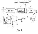
- FIGS 6 and 7 illustrate a vertical sync separator 50, embodying the invention, and using a surface acoustic wave (SAW) device 251 as a delay line.
- the composite video information is inputted into SAW 251 as a frequency modulated analogue signal rather than an amplitude modulated voltage.
- Composite video signal 29 with amplitude voltage variations is coupled at input terminal 34 to a voltage controlled oscillator (VCO) 70.
- VCO 70 produces a composite video voltage 229 that is frequency modulated in accordance with the input voltage amplitude variations.
- Frequency modulated composite video signal 229 is coupled to an input transducer 71 of surface acoustic wave delay line 251 which converts composite video signal 229 into a modulated acoustic wave that propagates along the surface of the substrate of device 251.
- frequency modulated composite video voltage V 229 fills the length of SAW 251, as illustrated in Figure 7.
- regions 301 and 306 for example, during the occurrence of the sync tip portions 101 and 106 of vertical sync pulse 57, the portions of frequency modulated composite sync voltage V 229 located in the regions 301 and 306 are relatively high frequency signals 229H, for example.
- regions. 401 and 406 for example, during the occurrence of the portions 201 and 206 of vertical sync pulse 57, the portions of frequency modulated composite sync voltage V 229 located in the regions 401 and 406 are relatively low frequency signals 229L.
- a sampling network 253 comprising interdigitated electrode fingers is deposited on the substrate of SAW 251.
- the spacing of the electrodes in regions 301 and 306 corresponds to a 1/2 wavelength separation related to the high frequency signals 229H.
- the spacing of the electrodes in regions 401 and 406 corresponds to a 1/2 wavelength separation related to the low frequency signals 229L.
- the output of the upper electrodes are coupled to and summed in a summing electrode line 72, and the output of the lower electrodes are coupled to and summed in a summing electrode line 73.
- SAW 251 functions as a pulse compression filter to produce a compressed pulse from the vertical sync information.
- Lines 72 and 73 are coupled to an envelope detector of a vertical sync detector circuit 254 to remove the high frequency components of the compressed output signal.
- a threshold comparator 78 produces an output vertical sync pulse 55' upon the occurrence of the vertical sync pulse within the composite video signals.
- the threshold level is determined by the adjustment of a wiper arm of a potentiometer 79.
- Envelope detector 74 may comprise a diode demodulator comprising a resistor 75 across lines 72 and 73, a diode 76 coupled to line 73 and a shunt capacitor 77 coupled to diode 76.
- the cathode of diode 76 is coupled to the negative input terminal of comparator 78.
- FIG. 8 illustrates a vertical sync separator circuit 50 embodying the invention, that is also capable of processing frequency modulated composite video signals but does not use a SAW device as a delay line.
- Amplitude modulated composite video voltage V 29 is transformed by a voltage controlled oscillator 70 into a frequency modulated composite video voltage V 22 , at a terminal 234.
- High frequency portions 229H of V 229 are developed during the occurrence of sync tip portions 101-106 of the vertical pulse 57, whereas the low frequency portions 229L of V 229 are developed during the occurrence of blanking level portions 201-206.
- Frequency modulated composite video voltage V 221 is inputted into a delay line 351 which may, for example, comprise a charge coupled device.
- the length of delay line 351 is selected such that during the occurrence of a vertical sync pulse 57, at time t 3 of Figure 3, regions 301-306 are filled with high frequency portions 229H of V 121 and regions 401-406 are filled with low frequency portions 229L.
- Sampling tap lines 501-506 are formed adjacent the beginning locations of regions 301-306 and sampling tap lines 601-606 are formed adjacent the beginning locations of regions 401 ⁇ 405.
- Taps 501-506 and 601-606 sample the frequency modulated composite video voltage V 229 as it passes through delay line 351.
- the sampled information at each of the taps of the delay line is coupled to a respective one of FET buffer amplifiers 701-712.
- At the output of each buffer amplifier is developed a frequency modulated voltage corresponding to V 229 .
- the output voltage of each successive amplifier however is phase delayed with respect to the output voltage of the previous amplifier.
- each of the FET buffer amplifiers 701-712 is coupled to a respective one of bandpass filters 801-812.
- Buffer amplifiers 701-712 function, in part, to match the high impedance requirements of the bandpass filters.
- the bandpass frequency of a given set of filters 801-812 is selected to pass only the high frequencies associated with portions 229H of V 121 if the given filter is coupled to tap lines 501-506 of regions 301-306, or to pass only the low frequencies associated with portions 229L or V 229 , if the given filter is coupled to tap lines 601-606 of regions 401-406.
- the outputs of all bandpass filters 801-812 are at a maximum.
- the outputs of the band-pass filters are summed in a summing circuit 80 after the high frequency components of the outputs are removed by envelope detectors 901-912, any one of which detectors may be of design similar to envelope detector 74 of Figure 6.
- the output of summing circuit 80 is thus a compressed pulse which is then coupled to an input terminal of a threshold comparator 81.
- the output of summing circuit 80 is a maximum, enabling comparator 81 to develop an output sync pulse 55' at a terminal 36.
- the threshold level of comparator 81 is adjusted by adjusting the wiper arm of a potentiometer 82.
- Delay line 351 need not be a semiconductor device but may, as illustrated in Figure 9, be constructed as a lumped LC coil 351', with taps 501-506 and 601-606 being coupled to appropriate locations along the coil.
- increased noise immunity can be obtained by increasing the delay of the delay line, so as to allow sampling of the composite video during the equalizing pulse intervals as well as the vertical synchronizing pulse intervals.
- a cost reduction may be obtained by decreasing the delay of the delay line and the number of taps, so long as adequate sensitivity for the application remains.
- the described sync separator may be used in conjunction with further signal processing, such as by a vertical count-down system for producing a deflection drive signal. Differences in amplitude between the response of taps near the input end of the delay line compared with that near the output end resulting from signal attenuation in the delay line may be compensated for by proper selection of the weighting resistors.
Landscapes
- Engineering & Computer Science (AREA)
- Multimedia (AREA)
- Signal Processing (AREA)
- Synchronizing For Television (AREA)
- Transmission And Conversion Of Sensor Element Output (AREA)
- Slot Machines And Peripheral Devices (AREA)
- Burglar Alarm Systems (AREA)
- Details Of Television Scanning (AREA)
Claims (15)
Priority Applications (1)
| Application Number | Priority Date | Filing Date | Title |
|---|---|---|---|
| AT80300958T ATE4950T1 (de) | 1979-04-04 | 1980-03-27 | Vertikal-synchronsignal-separator. |
Applications Claiming Priority (2)
| Application Number | Priority Date | Filing Date | Title |
|---|---|---|---|
| US06/026,814 US4240111A (en) | 1979-04-04 | 1979-04-04 | Vertical sync separator |
| US26814 | 1979-04-04 |
Publications (2)
| Publication Number | Publication Date |
|---|---|
| EP0017432A1 EP0017432A1 (fr) | 1980-10-15 |
| EP0017432B1 true EP0017432B1 (fr) | 1983-10-05 |
Family
ID=21833919
Family Applications (1)
| Application Number | Title | Priority Date | Filing Date |
|---|---|---|---|
| EP80300958A Expired EP0017432B1 (fr) | 1979-04-04 | 1980-03-27 | Séparateur d'un signal de synchronisation verticale |
Country Status (5)
| Country | Link |
|---|---|
| US (1) | US4240111A (fr) |
| EP (1) | EP0017432B1 (fr) |
| JP (1) | JPS6053986B2 (fr) |
| AT (1) | ATE4950T1 (fr) |
| DE (1) | DE3065115D1 (fr) |
Families Citing this family (7)
| Publication number | Priority date | Publication date | Assignee | Title |
|---|---|---|---|---|
| JPS56165469A (en) * | 1980-05-23 | 1981-12-19 | Sony Corp | Detecting method of vertical synchronous signal |
| US4583048A (en) * | 1985-02-26 | 1986-04-15 | Rca Corporation | MSK digital demodulator for burst communications |
| JPH06101804B2 (ja) * | 1985-09-25 | 1994-12-12 | ヤマハ株式会社 | 垂直同期タイミング信号発生回路 |
| US5249052A (en) * | 1987-02-14 | 1993-09-28 | Canon Kabushiki Kaisha | Image display system with compressed video signal recording and display |
| US5999222A (en) * | 1997-09-04 | 1999-12-07 | Hughes-Jvc Technology Corporation | Digital vertical sync separator |
| JP5185212B2 (ja) * | 2009-06-12 | 2013-04-17 | 株式会社東芝 | 色信号処理回路 |
| WO2023275177A1 (fr) * | 2021-06-30 | 2023-01-05 | Ambu A/S | Appareil de traitement vidéo avec atténuation d'effet de bruit |
Family Cites Families (9)
| Publication number | Priority date | Publication date | Assignee | Title |
|---|---|---|---|---|
| US2551250A (en) * | 1947-11-12 | 1951-05-01 | Gen Electric | Pulse discriminator |
| NL279259A (fr) * | 1961-06-05 | |||
| US3526714A (en) * | 1968-01-25 | 1970-09-01 | Bell Telephone Labor Inc | Television receiver synchronizing apparatus |
| US3751588A (en) * | 1972-06-02 | 1973-08-07 | Gte Sylvania Inc | Vertical synchronizing circuitry |
| US3909724A (en) * | 1973-06-26 | 1975-09-30 | Addressograph Multigraph | Start bit detector and data strober for asynchronous receiver |
| US3878335A (en) * | 1973-10-18 | 1975-04-15 | Rca Corp | Digital synchronization system |
| FR2283592A1 (fr) * | 1974-08-27 | 1976-03-26 | Thomson Csf | Dispositif extracteur de synchronisation et systeme de transmission d'informations comportant un tel dispositif |
| US3991379A (en) * | 1975-06-03 | 1976-11-09 | United Technologies Corporation | Logic level decoding circuit |
| DE2607433C3 (de) * | 1976-02-24 | 1980-01-17 | Siemens Ag | Digitaler Korrelationsempfänger |
-
1979
- 1979-04-04 US US06/026,814 patent/US4240111A/en not_active Expired - Lifetime
-
1980
- 1980-03-27 EP EP80300958A patent/EP0017432B1/fr not_active Expired
- 1980-03-27 DE DE8080300958T patent/DE3065115D1/de not_active Expired
- 1980-03-27 AT AT80300958T patent/ATE4950T1/de not_active IP Right Cessation
- 1980-04-03 JP JP55044535A patent/JPS6053986B2/ja not_active Expired
Also Published As
| Publication number | Publication date |
|---|---|
| JPS55135470A (en) | 1980-10-22 |
| EP0017432A1 (fr) | 1980-10-15 |
| ATE4950T1 (de) | 1983-10-15 |
| JPS6053986B2 (ja) | 1985-11-28 |
| DE3065115D1 (en) | 1983-11-10 |
| US4240111A (en) | 1980-12-16 |
Similar Documents
| Publication | Publication Date | Title |
|---|---|---|
| US4667235A (en) | Teletext decoder | |
| CA1165434A (fr) | Circuit pour capter les signaux | |
| US4115812A (en) | Automatic gain control circuit | |
| EP0017432B1 (fr) | Séparateur d'un signal de synchronisation verticale | |
| US4128848A (en) | Automatic ghost-suppression system | |
| US4295161A (en) | Keyed noise filter in a television receiver | |
| FI61596C (fi) | Krets foer automatisk foerstaerkningsreglering foer televisionsapparater | |
| US4275420A (en) | Television receiver with a ghost detector | |
| JPH0532948B2 (fr) | ||
| US4513321A (en) | Black level clamp for television signals | |
| EP0047528B1 (fr) | Circuit de commande de la tonalité vidéo | |
| EP0573295B1 (fr) | Circuit de détection de niveau et circuit de contrÔle automatique de couleur | |
| US4047223A (en) | Frequency scanning automatic phase control system | |
| US4544943A (en) | Stabilized color television subcarrier regenerator circuit | |
| US4363035A (en) | Method and apparatus for signal pick-up from semiconductor image or line sensors | |
| US4682087A (en) | Apparatus for controlling amplitude of vertical deflection signal | |
| US4148068A (en) | Television synchronizing signal separating circuit | |
| GB2030809A (en) | Signal sampler | |
| US4621288A (en) | Reference time detecting circuit | |
| US2797258A (en) | Sync separator | |
| US4216502A (en) | Peak detector circuit | |
| CA1070822A (fr) | Commande automatique de phase horizontale a vitesse variable | |
| US5113257A (en) | Line synchronising circuit | |
| KR890000284B1 (ko) | 수평 발진기 | |
| JPS5851675A (ja) | Agc回路 |
Legal Events
| Date | Code | Title | Description |
|---|---|---|---|
| PUAI | Public reference made under article 153(3) epc to a published international application that has entered the european phase |
Free format text: ORIGINAL CODE: 0009012 |
|
| AK | Designated contracting states |
Designated state(s): AT DE FR GB IT |
|
| 17P | Request for examination filed |
Effective date: 19810323 |
|
| ITF | It: translation for a ep patent filed | ||
| GRAA | (expected) grant |
Free format text: ORIGINAL CODE: 0009210 |
|
| AK | Designated contracting states |
Designated state(s): AT DE FR GB IT |
|
| REF | Corresponds to: |
Ref document number: 4950 Country of ref document: AT Date of ref document: 19831015 Kind code of ref document: T |
|
| REF | Corresponds to: |
Ref document number: 3065115 Country of ref document: DE Date of ref document: 19831110 |
|
| ET | Fr: translation filed | ||
| PGFP | Annual fee paid to national office [announced via postgrant information from national office to epo] |
Ref country code: DE Payment date: 19840109 Year of fee payment: 5 |
|
| PGFP | Annual fee paid to national office [announced via postgrant information from national office to epo] |
Ref country code: FR Payment date: 19840111 Year of fee payment: 5 |
|
| PLBE | No opposition filed within time limit |
Free format text: ORIGINAL CODE: 0009261 |
|
| STAA | Information on the status of an ep patent application or granted ep patent |
Free format text: STATUS: NO OPPOSITION FILED WITHIN TIME LIMIT |
|
| 26N | No opposition filed | ||
| PGFP | Annual fee paid to national office [announced via postgrant information from national office to epo] |
Ref country code: AT Payment date: 19860327 Year of fee payment: 7 |
|
| PG25 | Lapsed in a contracting state [announced via postgrant information from national office to epo] |
Ref country code: AT Effective date: 19870327 |
|
| GBPC | Gb: european patent ceased through non-payment of renewal fee | ||
| PG25 | Lapsed in a contracting state [announced via postgrant information from national office to epo] |
Ref country code: FR Free format text: LAPSE BECAUSE OF NON-PAYMENT OF DUE FEES Effective date: 19871130 |
|
| PG25 | Lapsed in a contracting state [announced via postgrant information from national office to epo] |
Ref country code: DE Effective date: 19871201 |
|
| REG | Reference to a national code |
Ref country code: FR Ref legal event code: ST |
|
| PG25 | Lapsed in a contracting state [announced via postgrant information from national office to epo] |
Ref country code: GB Effective date: 19881118 |