EP0017585A1 - Verfahren und System zum Betrieb eines adressierbaren Speichers, wobei nach Belieben den Speicherdaten Erweiterungen zugefügt werden können - Google Patents
Verfahren und System zum Betrieb eines adressierbaren Speichers, wobei nach Belieben den Speicherdaten Erweiterungen zugefügt werden können Download PDFInfo
- Publication number
- EP0017585A1 EP0017585A1 EP80400440A EP80400440A EP0017585A1 EP 0017585 A1 EP0017585 A1 EP 0017585A1 EP 80400440 A EP80400440 A EP 80400440A EP 80400440 A EP80400440 A EP 80400440A EP 0017585 A1 EP0017585 A1 EP 0017585A1
- Authority
- EP
- European Patent Office
- Prior art keywords
- data
- memory
- extensions
- additional data
- extension
- Prior art date
- Legal status (The legal status is an assumption and is not a legal conclusion. Google has not performed a legal analysis and makes no representation as to the accuracy of the status listed.)
- Withdrawn
Links
Images


Classifications
-
- G—PHYSICS
- G06—COMPUTING OR CALCULATING; COUNTING
- G06F—ELECTRIC DIGITAL DATA PROCESSING
- G06F9/00—Arrangements for program control, e.g. control units
- G06F9/06—Arrangements for program control, e.g. control units using stored programs, i.e. using an internal store of processing equipment to receive or retain programs
- G06F9/30—Arrangements for executing machine instructions, e.g. instruction decode
- G06F9/30181—Instruction operation extension or modification
-
- G—PHYSICS
- G06—COMPUTING OR CALCULATING; COUNTING
- G06F—ELECTRIC DIGITAL DATA PROCESSING
- G06F12/00—Accessing, addressing or allocating within memory systems or architectures
- G06F12/02—Addressing or allocation; Relocation
- G06F12/04—Addressing variable-length words or parts of words
-
- G—PHYSICS
- G06—COMPUTING OR CALCULATING; COUNTING
- G06F—ELECTRIC DIGITAL DATA PROCESSING
- G06F12/00—Accessing, addressing or allocating within memory systems or architectures
- G06F12/02—Addressing or allocation; Relocation
- G06F12/06—Addressing a physical block of locations, e.g. base addressing, module addressing, memory dedication
- G06F12/0638—Combination of memories, e.g. ROM and RAM such as to permit replacement or supplementing of words in one module by words in another module
-
- G—PHYSICS
- G06—COMPUTING OR CALCULATING; COUNTING
- G06F—ELECTRIC DIGITAL DATA PROCESSING
- G06F9/00—Arrangements for program control, e.g. control units
- G06F9/06—Arrangements for program control, e.g. control units using stored programs, i.e. using an internal store of processing equipment to receive or retain programs
- G06F9/30—Arrangements for executing machine instructions, e.g. instruction decode
- G06F9/34—Addressing or accessing the instruction operand or the result ; Formation of operand address; Addressing modes
- G06F9/342—Extension of operand address space
Definitions
- This invention also applies to automata in general when, for example, certain operations must be accompanied by additional operations. It's the case, for example, of a machine controlled by a microprocessor which to execute an operation needs the cooperation of an additional means such as for example a supply of material or fluid.
- This additional means is defined by additional data associated with the data relating to the operation.
- additional data could consist of a drill change order with indication of the characteristics of the drill.
- the processing unit can thus store additional data in the memory of the extensions.
- said transmission of additional data to said user means takes place at the request of the aforementioned user means.
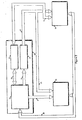
- This set of signals applied to the data memory (24) and to the extension means (25) will cause these 2 organs (24) and (25) to execute a write cycle.
- this write cycle will store the data placed on the omnibus (26) of the data in the location of the memory (24) of the data defined by the address placed on the omnibus (23). addresses.
- this write cycle command will place the extension received previously on the extensions bus (31) deferred.
- this writing cycle causes the storage of the extension placed on the omnibus (31) of the deferred extensions in the location of the means (25) of extension defined by the address placed on the addresses bus (23).
- the means (25) of extension after an operation of reading the content of a location defined by an address, warn the means (28) users in the event of detection the presence of an extension associated with the called address. For this, they place a signal on the monitoring omnibus (29) informing the user means (28) of the existence of an extension associated with the data item called.
- This information of the means (28) users of the existence of this extension avoids having to request a special cycle from the intermediate means (30).
- the intermediate means (30) consist of an addressable device similar to those used to connect the user means (28) of data with peripheral means: the intermediate means (30) are considered by the user means (28) as a particular peripheral means.
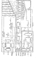
- FIG. 4 represents a preferred embodiment of the invention produced around a MOTOROLA MC 6800 microprocessor.
- the means (28) of use consist of a clock (49) of the MOTOROLA MC 6871 type and of a microprocessor (48) of the MOTOROLA MC 6800 type.
- This conditioner (109) receives on its terminal (1) the clock signal " ⁇ 3 " coming from the internal clock (107), on its terminal (2) a signal emitted by the output (3) of the circuit (108 ) OU-EXCLUSIVE and on its terminal (3) a selection signal emitted by the qualifier writing controller (69).
- the OU-EXCLUSIVE circuit (108) receives on its input (1) . the value of the bit to store, in the case of a write, sent by the controller (69) for writing the extensions.
- the terminal (2) of the input-output circuit (103) supplies the input of the OR-EXCLUSIVE circuit (104).
- This OU-EXCLUSIVE circuit (104) receives on its input (2) a signal emitted by the internal clock (107).
- the block (137) for controlling interruptions informs the write unification controller (69) by sending a signal on the link (131) which arrives at the terminal (+ ) of the bistable (124) which is located in the block (90) for checking the uniqueness of writing.
- the bistable (124) switches and its output (1) goes to a high level on the falling edge of the clock signal # 2 .
- This high level means for the write uniqueness control block (90) that the configuration of the extension is available at the output of the interface adaptation circuit (70) on the bus (152).
Landscapes
- Engineering & Computer Science (AREA)
- Theoretical Computer Science (AREA)
- Software Systems (AREA)
- Physics & Mathematics (AREA)
- General Engineering & Computer Science (AREA)
- General Physics & Mathematics (AREA)
- Bus Control (AREA)
- Techniques For Improving Reliability Of Storages (AREA)
- Information Retrieval, Db Structures And Fs Structures Therefor (AREA)
- Debugging And Monitoring (AREA)
- Memory System (AREA)
Applications Claiming Priority (2)
| Application Number | Priority Date | Filing Date | Title |
|---|---|---|---|
| FR7908714 | 1979-04-06 | ||
| FR7908714A FR2453467A1 (fr) | 1979-04-06 | 1979-04-06 | Procede et systeme d'exploitation d'une memoire adressable permettant d'associer a volonte des extensions aux donnees contenues dans la memoire |
Publications (1)
| Publication Number | Publication Date |
|---|---|
| EP0017585A1 true EP0017585A1 (de) | 1980-10-15 |
Family
ID=9224038
Family Applications (1)
| Application Number | Title | Priority Date | Filing Date |
|---|---|---|---|
| EP80400440A Withdrawn EP0017585A1 (de) | 1979-04-06 | 1980-04-02 | Verfahren und System zum Betrieb eines adressierbaren Speichers, wobei nach Belieben den Speicherdaten Erweiterungen zugefügt werden können |
Country Status (4)
| Country | Link |
|---|---|
| US (1) | US4356548A (de) |
| EP (1) | EP0017585A1 (de) |
| JP (1) | JPS5614361A (de) |
| FR (1) | FR2453467A1 (de) |
Cited By (1)
| Publication number | Priority date | Publication date | Assignee | Title |
|---|---|---|---|---|
| EP0020983B1 (de) * | 1979-06-11 | 1984-04-18 | International Business Machines Corporation | Speichersystem mit einer serienmässigen Speichervorrichtung |
Families Citing this family (2)
| Publication number | Priority date | Publication date | Assignee | Title |
|---|---|---|---|---|
| JPS62157947A (ja) * | 1985-12-28 | 1987-07-13 | Yamatake Honeywell Co Ltd | 制御装置 |
| FR2749681B1 (fr) * | 1996-06-10 | 1998-07-10 | Bull Sa | Circuit pour transborder des donnees entre memoires distantes et calculateur comprenant un tel circuit |
Citations (4)
| Publication number | Priority date | Publication date | Assignee | Title |
|---|---|---|---|---|
| US2843841A (en) * | 1954-09-20 | 1958-07-15 | Internat Telemeter Corp | Information storage system |
| GB1254929A (en) * | 1969-03-26 | 1971-11-24 | Standard Telephones Cables Ltd | Improvements in or relating to digital computers |
| DE2714314A1 (de) * | 1977-03-31 | 1978-10-05 | Licentia Gmbh | Datenverarbeitende vorrichtung mit einem datenspeicher |
| FR2412107A1 (fr) * | 1977-12-16 | 1979-07-13 | Option | Systeme a logique programmee |
Family Cites Families (9)
| Publication number | Priority date | Publication date | Assignee | Title |
|---|---|---|---|---|
| US3434116A (en) * | 1966-06-15 | 1969-03-18 | Ibm | Scheme for circumventing bad memory cells |
| US3633175A (en) * | 1969-05-15 | 1972-01-04 | Honeywell Inc | Defect-tolerant digital memory system |
| US3725872A (en) * | 1971-03-03 | 1973-04-03 | Burroughs Corp | Data processing system having status indicating and storage means |
| US3818459A (en) * | 1972-12-19 | 1974-06-18 | Dimensional Syst Inc | Auxiliary memory interface system |
| US3803560A (en) * | 1973-01-03 | 1974-04-09 | Honeywell Inf Systems | Technique for detecting memory failures and to provide for automatically for reconfiguration of the memory modules of a memory system |
| US3828327A (en) * | 1973-04-30 | 1974-08-06 | Ibm | Simplified storage protection and address translation under system mode control in a data processing system |
| US3893084A (en) * | 1973-05-01 | 1975-07-01 | Digital Equipment Corp | Memory access control system |
| US3934227A (en) * | 1973-12-05 | 1976-01-20 | Digital Computer Controls, Inc. | Memory correction system |
| US4058851A (en) * | 1976-10-18 | 1977-11-15 | Sperry Rand Corporation | Conditional bypass of error correction for dual memory access time selection |
-
1979
- 1979-04-06 FR FR7908714A patent/FR2453467A1/fr active Granted
-
1980
- 1980-03-28 US US06/135,079 patent/US4356548A/en not_active Expired - Lifetime
- 1980-04-02 EP EP80400440A patent/EP0017585A1/de not_active Withdrawn
- 1980-04-07 JP JP4478280A patent/JPS5614361A/ja active Pending
Patent Citations (4)
| Publication number | Priority date | Publication date | Assignee | Title |
|---|---|---|---|---|
| US2843841A (en) * | 1954-09-20 | 1958-07-15 | Internat Telemeter Corp | Information storage system |
| GB1254929A (en) * | 1969-03-26 | 1971-11-24 | Standard Telephones Cables Ltd | Improvements in or relating to digital computers |
| DE2714314A1 (de) * | 1977-03-31 | 1978-10-05 | Licentia Gmbh | Datenverarbeitende vorrichtung mit einem datenspeicher |
| FR2412107A1 (fr) * | 1977-12-16 | 1979-07-13 | Option | Systeme a logique programmee |
Non-Patent Citations (1)
| Title |
|---|
| IBM TECHNICAL DISCLOSURE BULLETIN, vol. 22, no. 1, juin 1979, New York, US, PARTRIDGE: "Full memory compare processor monitor circuit", pages 182-183. * |
Cited By (1)
| Publication number | Priority date | Publication date | Assignee | Title |
|---|---|---|---|---|
| EP0020983B1 (de) * | 1979-06-11 | 1984-04-18 | International Business Machines Corporation | Speichersystem mit einer serienmässigen Speichervorrichtung |
Also Published As
| Publication number | Publication date |
|---|---|
| FR2453467B1 (de) | 1983-08-19 |
| US4356548A (en) | 1982-10-26 |
| FR2453467A1 (fr) | 1980-10-31 |
| JPS5614361A (en) | 1981-02-12 |
Similar Documents
| Publication | Publication Date | Title |
|---|---|---|
| FR2539528A1 (fr) | Systeme a microprocesseur comportant deux processeurs | |
| FR2478845A1 (fr) | Equipement de traitement de donnees comportant un appareil de diagnostic, et procede permettant d'etablir une communication entre l'appareil de diagnostic et un processeur principal de l'equipement | |
| CH637228A5 (fr) | Dispositif de commande d'une machine ou d'une installation. | |
| FR2500187A1 (fr) | Unite centrale de traitement de donnees | |
| FR2612313A1 (fr) | Selecteur programmable d'options | |
| EP0005722A1 (de) | Auswahlsystem für Vorrangsschnittstellen | |
| EP0366520B1 (de) | Datenübertragungsnetzwerk für Multiprozessorsysteme | |
| EP0837396A1 (de) | Atomare Operation in Fernspeicher und Vorrichtung zur Durchführung der Operation | |
| FR2765706A1 (fr) | Lecteur de cartes a puces a protocole de transmission rapide | |
| EP0017586B1 (de) | Datenverarbeitungseinrichtung mit zwei Speichern mit direktem Zugriff, die sowohl in Lese- wie in Schreibmodus zusammenarbeiten | |
| EP0769748A1 (de) | Mikroprozessorgewidmete integrierbare DDC-Zelle | |
| EP0017585A1 (de) | Verfahren und System zum Betrieb eines adressierbaren Speichers, wobei nach Belieben den Speicherdaten Erweiterungen zugefügt werden können | |
| FR2759178A1 (fr) | Circuit de gestion de memoire dans un environnement multi-utilisateurs avec requete et priorite d'acces | |
| EP0017584A1 (de) | Verfahren und System zum Betrieb eines adressierbaren Speichers, wobei nach Belieben den Speicherdaten Eigenschaftswörter zugefügt werden können | |
| FR2744539A1 (fr) | Systeme et procede de traitement par augmentation du nombre d'entrees de donnees | |
| EP0344035B1 (de) | Digitales Nachrichtenübertragungsnetz zwischen mehreren Endgeräten | |
| EP0632622A1 (de) | Verfahren zur zeitlichen Einteilung von zu Nachrichten gehörenden Zellmissionen sowie Vorrichtung zur Durchführung dieses Verfahrens | |
| EP0011540B1 (de) | Ein-/Ausgabe-Schnittstelle zwischen einem Datenvermittler und mehreren Übertragungsleitungen | |
| EP0589743B1 (de) | Modulare Vorrichtung zum Koppeln und zum Multiplexen von unterschiedlichen Bussen | |
| FR2490367A1 (fr) | Coupleur de supports electroniques amovibles | |
| EP0269167B1 (de) | Integrierte Schaltung und Verfahren für Zahlenverarbeitung in einem Modul mit automatischer Taktsteuerung | |
| EP0561699B1 (de) | Kommunikationsverfahren für eine programmierbare industrielle Steuerung und Schnittstelle für die Ausführung des Verfahrens | |
| EP0466555A1 (de) | Lokales Netzwerk für Interkommunikation zwischen Datenverarbeitungsmodulen | |
| FR2754924A1 (fr) | Circuit de memoire tampon d'entree/sortie capable de minimiser le transfert de donnees requis dans les operations de tamponnage d'entree et de sortie | |
| FR2538140A1 (fr) | Dispositif de couplage de bus pour systeme de traitement de donnees a bus multiples |
Legal Events
| Date | Code | Title | Description |
|---|---|---|---|
| PUAI | Public reference made under article 153(3) epc to a published international application that has entered the european phase |
Free format text: ORIGINAL CODE: 0009012 |
|
| AK | Designated contracting states |
Designated state(s): DE GB IT |
|
| 17P | Request for examination filed |
Effective date: 19801015 |
|
| STAA | Information on the status of an ep patent application or granted ep patent |
Free format text: STATUS: THE APPLICATION HAS BEEN WITHDRAWN |
|
| 18W | Application withdrawn |
Withdrawal date: 19830128 |
|
| RIN1 | Information on inventor provided before grant (corrected) |
Inventor name: BAVOUX, ROBERT JULES ADOLPHE Inventor name: SALKAZANOV, PIERRE Inventor name: LEMAIRE, FRANCIS RENE JEAN-MARIE |