EP0019208A1 - Procédé pour la fabrication d'un dispositif d'affichage électro-optique passif - Google Patents
Procédé pour la fabrication d'un dispositif d'affichage électro-optique passif Download PDFInfo
- Publication number
- EP0019208A1 EP0019208A1 EP80102500A EP80102500A EP0019208A1 EP 0019208 A1 EP0019208 A1 EP 0019208A1 EP 80102500 A EP80102500 A EP 80102500A EP 80102500 A EP80102500 A EP 80102500A EP 0019208 A1 EP0019208 A1 EP 0019208A1
- Authority
- EP
- European Patent Office
- Prior art keywords
- back electrode
- deposited
- layer
- electrode
- applies
- Prior art date
- Legal status (The legal status is an assumption and is not a legal conclusion. Google has not performed a legal analysis and makes no representation as to the accuracy of the status listed.)
- Ceased
Links
- 238000004519 manufacturing process Methods 0.000 title claims abstract description 6
- 238000000034 method Methods 0.000 claims abstract description 32
- 239000004973 liquid crystal related substance Substances 0.000 claims abstract description 12
- 229910052782 aluminium Inorganic materials 0.000 claims abstract description 11
- XAGFODPZIPBFFR-UHFFFAOYSA-N aluminium Chemical compound [Al] XAGFODPZIPBFFR-UHFFFAOYSA-N 0.000 claims abstract description 9
- 229910045601 alloy Inorganic materials 0.000 claims abstract description 7
- 239000000956 alloy Substances 0.000 claims abstract description 7
- 229910052709 silver Inorganic materials 0.000 claims abstract description 7
- 229910052751 metal Inorganic materials 0.000 claims abstract description 6
- 239000002184 metal Substances 0.000 claims abstract description 6
- 238000000576 coating method Methods 0.000 claims abstract description 4
- 150000002739 metals Chemical class 0.000 claims abstract description 4
- 238000004544 sputter deposition Methods 0.000 claims description 9
- 238000000151 deposition Methods 0.000 claims description 7
- 230000008021 deposition Effects 0.000 claims description 6
- 239000000975 dye Substances 0.000 claims description 6
- 230000008020 evaporation Effects 0.000 claims description 3
- 238000001704 evaporation Methods 0.000 claims description 3
- 229910016570 AlCu Inorganic materials 0.000 claims description 2
- 229910017141 AlTa Inorganic materials 0.000 claims description 2
- 229910002711 AuNi Inorganic materials 0.000 claims description 2
- 229910002535 CuZn Inorganic materials 0.000 claims description 2
- 229910001030 Iron–nickel alloy Inorganic materials 0.000 claims description 2
- VNNRSPGTAMTISX-UHFFFAOYSA-N chromium nickel Chemical compound [Cr].[Ni] VNNRSPGTAMTISX-UHFFFAOYSA-N 0.000 claims description 2
- 239000011248 coating agent Substances 0.000 claims description 2
- 229910052737 gold Inorganic materials 0.000 claims description 2
- 230000000873 masking effect Effects 0.000 claims description 2
- 229910001120 nichrome Inorganic materials 0.000 claims description 2
- 230000003647 oxidation Effects 0.000 claims description 2
- 238000007254 oxidation reaction Methods 0.000 claims description 2
- 238000005546 reactive sputtering Methods 0.000 claims description 2
- 229910052802 copper Inorganic materials 0.000 claims 2
- 229910052715 tantalum Inorganic materials 0.000 claims 2
- 239000004215 Carbon black (E152) Substances 0.000 claims 1
- -1 CoGd Inorganic materials 0.000 claims 1
- 229910052688 Gadolinium Inorganic materials 0.000 claims 1
- 230000002745 absorbent Effects 0.000 claims 1
- 239000002250 absorbent Substances 0.000 claims 1
- 229910052804 chromium Inorganic materials 0.000 claims 1
- 229930195733 hydrocarbon Natural products 0.000 claims 1
- 150000002430 hydrocarbons Chemical class 0.000 claims 1
- 229910052738 indium Inorganic materials 0.000 claims 1
- 229910052742 iron Inorganic materials 0.000 claims 1
- 229910052745 lead Inorganic materials 0.000 claims 1
- 229910052749 magnesium Inorganic materials 0.000 claims 1
- 229910052759 nickel Inorganic materials 0.000 claims 1
- 229910052718 tin Inorganic materials 0.000 claims 1
- 229910052725 zinc Inorganic materials 0.000 claims 1
- 239000000758 substrate Substances 0.000 abstract description 15
- 239000000463 material Substances 0.000 abstract description 5
- 239000004332 silver Substances 0.000 abstract description 5
- 239000004411 aluminium Substances 0.000 abstract description 3
- 230000001419 dependent effect Effects 0.000 abstract description 2
- 239000000654 additive Substances 0.000 abstract 1
- 230000000996 additive effect Effects 0.000 abstract 1
- 239000003086 colorant Substances 0.000 description 6
- BQCADISMDOOEFD-UHFFFAOYSA-N Silver Chemical compound [Ag] BQCADISMDOOEFD-UHFFFAOYSA-N 0.000 description 5
- 239000013078 crystal Substances 0.000 description 3
- 238000010586 diagram Methods 0.000 description 3
- 238000010410 dusting Methods 0.000 description 3
- 230000000694 effects Effects 0.000 description 3
- 239000000203 mixture Substances 0.000 description 3
- XKRFYHLGVUSROY-UHFFFAOYSA-N Argon Chemical compound [Ar] XKRFYHLGVUSROY-UHFFFAOYSA-N 0.000 description 2
- KRHYYFGTRYWZRS-UHFFFAOYSA-N Fluorane Chemical compound F KRHYYFGTRYWZRS-UHFFFAOYSA-N 0.000 description 2
- 230000000295 complement effect Effects 0.000 description 2
- 239000010931 gold Substances 0.000 description 2
- 239000011261 inert gas Substances 0.000 description 2
- 150000002500 ions Chemical class 0.000 description 2
- 239000001301 oxygen Substances 0.000 description 2
- 229910052760 oxygen Inorganic materials 0.000 description 2
- 239000000126 substance Substances 0.000 description 2
- MYMOFIZGZYHOMD-UHFFFAOYSA-N Dioxygen Chemical compound O=O MYMOFIZGZYHOMD-UHFFFAOYSA-N 0.000 description 1
- 239000004988 Nematic liquid crystal Substances 0.000 description 1
- 230000001133 acceleration Effects 0.000 description 1
- 229910052786 argon Inorganic materials 0.000 description 1
- QVGXLLKOCUKJST-UHFFFAOYSA-N atomic oxygen Chemical compound [O] QVGXLLKOCUKJST-UHFFFAOYSA-N 0.000 description 1
- 230000015572 biosynthetic process Effects 0.000 description 1
- 239000004020 conductor Substances 0.000 description 1
- 230000007423 decrease Effects 0.000 description 1
- 238000011161 development Methods 0.000 description 1
- 230000018109 developmental process Effects 0.000 description 1
- 239000007789 gas Substances 0.000 description 1
- PCHJSUWPFVWCPO-UHFFFAOYSA-N gold Chemical compound [Au] PCHJSUWPFVWCPO-UHFFFAOYSA-N 0.000 description 1
- 238000010438 heat treatment Methods 0.000 description 1
- 230000003116 impacting effect Effects 0.000 description 1
- 238000011835 investigation Methods 0.000 description 1
- 229910052756 noble gas Inorganic materials 0.000 description 1
- TWNQGVIAIRXVLR-UHFFFAOYSA-N oxo(oxoalumanyloxy)alumane Chemical compound O=[Al]O[Al]=O TWNQGVIAIRXVLR-UHFFFAOYSA-N 0.000 description 1
- 239000002245 particle Substances 0.000 description 1
- 238000001259 photo etching Methods 0.000 description 1
- 238000001953 recrystallisation Methods 0.000 description 1
- 238000007788 roughening Methods 0.000 description 1
- 210000002023 somite Anatomy 0.000 description 1
- 238000003892 spreading Methods 0.000 description 1
- 230000003746 surface roughness Effects 0.000 description 1
- 239000000725 suspension Substances 0.000 description 1
Images


Classifications
-
- G—PHYSICS
- G02—OPTICS
- G02F—OPTICAL DEVICES OR ARRANGEMENTS FOR THE CONTROL OF LIGHT BY MODIFICATION OF THE OPTICAL PROPERTIES OF THE MEDIA OF THE ELEMENTS INVOLVED THEREIN; NON-LINEAR OPTICS; FREQUENCY-CHANGING OF LIGHT; OPTICAL LOGIC ELEMENTS; OPTICAL ANALOGUE/DIGITAL CONVERTERS
- G02F1/00—Devices or arrangements for the control of the intensity, colour, phase, polarisation or direction of light arriving from an independent light source, e.g. switching, gating or modulating; Non-linear optics
- G02F1/01—Devices or arrangements for the control of the intensity, colour, phase, polarisation or direction of light arriving from an independent light source, e.g. switching, gating or modulating; Non-linear optics for the control of the intensity, phase, polarisation or colour
- G02F1/13—Devices or arrangements for the control of the intensity, colour, phase, polarisation or direction of light arriving from an independent light source, e.g. switching, gating or modulating; Non-linear optics for the control of the intensity, phase, polarisation or colour based on liquid crystals, e.g. single liquid crystal display cells
- G02F1/133—Constructional arrangements; Operation of liquid crystal cells; Circuit arrangements
- G02F1/1333—Constructional arrangements; Manufacturing methods
- G02F1/1343—Electrodes
- G02F1/13439—Electrodes characterised by their electrical, optical, physical properties; materials therefor; method of making
-
- G—PHYSICS
- G02—OPTICS
- G02F—OPTICAL DEVICES OR ARRANGEMENTS FOR THE CONTROL OF LIGHT BY MODIFICATION OF THE OPTICAL PROPERTIES OF THE MEDIA OF THE ELEMENTS INVOLVED THEREIN; NON-LINEAR OPTICS; FREQUENCY-CHANGING OF LIGHT; OPTICAL LOGIC ELEMENTS; OPTICAL ANALOGUE/DIGITAL CONVERTERS
- G02F1/00—Devices or arrangements for the control of the intensity, colour, phase, polarisation or direction of light arriving from an independent light source, e.g. switching, gating or modulating; Non-linear optics
- G02F1/01—Devices or arrangements for the control of the intensity, colour, phase, polarisation or direction of light arriving from an independent light source, e.g. switching, gating or modulating; Non-linear optics for the control of the intensity, phase, polarisation or colour
- G02F1/13—Devices or arrangements for the control of the intensity, colour, phase, polarisation or direction of light arriving from an independent light source, e.g. switching, gating or modulating; Non-linear optics for the control of the intensity, phase, polarisation or colour based on liquid crystals, e.g. single liquid crystal display cells
- G02F1/133—Constructional arrangements; Operation of liquid crystal cells; Circuit arrangements
- G02F1/1333—Constructional arrangements; Manufacturing methods
- G02F1/1335—Structural association of cells with optical devices, e.g. polarisers or reflectors
- G02F1/133553—Reflecting elements
Definitions
- the invention relates to a method according to the preamble of claim 1 and also relates to a display device produced by such a method. Such a display is described in DE-CS 28 13 007.
- the rear electrode In the case of a display whose optically effective medium is switched between the "colored” and “transparent” states, the rear electrode should be designed to be diffusely scattering. Because then you no longer need a separate reflector and also get a parallax-free, easy-to-read display without annoying reflections.
- the invention has for its object to provide a method of the type mentioned, with which a diffusely scattering back electrode can be produced without special effort, which has good conductivity and a high reflection factor and can also be designed white or colored as required. According to the invention, this object is achieved by a method having the features of patent claim 1.
- the proposed solution is based on the following observation. If a material is sputtered onto a substrate, the deposited layer, which remains bare under normal sputtering conditions, surprisingly obtains a matt appearance if the layer thickness and the substrate temperature are above certain values.
- the two parameters are interrelated: with larger layer thicknesses, smaller substrate temperatures are sufficient, while smaller layer thicknesses require higher substrate temperatures.
- the layer becomes matt when the product of layer thickness and substrate temperature exceeds a critical value.
- This limit value is primarily determined by the material used, but also depends on other variables such as the type and pressure of the dusting gas, the acceleration voltage, the nature of the substrate surface and the sputtering rate. Basically, the same relationships also exist when the metal is vapor-deposited. However, the limit value mentioned here is greater for conventional evaporation rates and, moreover, more dependent on the deposition rate than for sputtering.
- Electron microscopic investigations have shown that crystallites form in the deposited layer, which are many times more extensive in the layer plane than in the direction of the layer normal, grow with increasing layer thickness and / or substrate temperature and, when the layer diffuses, dimensions of size of the light wavelength.
- Aluminum and silver are particularly suitable for the proposed process, in which the conditions contained in claims 6 to 8 should be observed.
- claim 4 all materials are enumerated, which come into question for the present method, sorted according to their importance for the present purposes.
- alloys claim 5
- the back electrode receives a particularly pronounced, uniform surface grain and adheres well to its carrier plate if the base is previously chemically etched, for example with hydrofluoric acid, or sputter-etched, for example with argon.
- Another possibility for improving the spreading power is to pollinate in the manner characterized in claim 11.
- Such a sputtering promotes recrystallization, because now plasma ions can also hit the growing layer and release their energy there, and also intensify any unevenness in the layer, because a profiled surface leads to field strength concentrations and corresponding ion bundling.
- the last-mentioned effect which can be observed above all in alloys with partners with different dusting rates, can be further increased by the measure mentioned in claim 12.
- Au looks gold-colored;
- AlCu has colors between white, yellow and reddish brown;
- CuZn acts between red-brown, yellow and gray;
- NiFe is brown, for example in the composition Ni 80 Fe 20 ;
- NiCr looks, for example, with a balanced composition silver gray;
- AlTa appears with a Ta content of up to about 15% by weight between white and gray;
- CoGd is gray and
- AuNi has colors between gold and gray, depending on the proportion of the two components.
- a variety of colors could be formed by suitably designed coatings on the back electrode, which can be produced by reactive sputtering, by thermal or by anodic oxidation. Manufacturing processes which are particularly suitable for this are the subject of claims 13 to 15. It has been shown that such overlays which appear colored due to interference effects, can deliver colors even on rough surfaces. You can also influence the color brightness by choosing the grain size, because with increasing surface roughness the colors become darker. The layer will eventually turn black if that hits. Light is completely absorbed by multiple scattering.
- the production method according to the invention is used above all in "absorptive" displays, the switchable medium of which could be, for example, a (dipole) suspension or a liquid crystal substance with embedded dichroic dyes.
- the back electrode can also act as an orientation layer.
- the vertical alignment of the plates required in absorptive liquid crystal displays is induced, for example, by a sputtered-on aluminum oxide film.
- the carrier plates. are each provided with electrically conductive coverings on the inside.
- the covering of the front plate consists of several, transparent segments (front electrode segments 6), the rear plate covering is a single electrode (back electrode 7) which diffusely reflects in a certain color.
- the front electrodes are manufactured in the usual way and covered with a homeotropically orientated layer (not shown).
- the embodiment shown in FIG. 2 differs from the example of FIG. 1 essentially in that the back electrode consists of several segments (back electrode segments 8) and the front electrode designated 9 is made in one piece and that. the inside of the front plate is also covered with a diffusely reflective layer (aperture layer 11).
- the screen is made of the same material as the back electrode segments and covers the complementary surface.
- the back electrode can be segmented in different ways: Either you first cut out the entire surface and then selectively remove the surface that is complementary to the segments, for example by photoetching or in one of the common lifting techniques, or you cut off right away using a mask.
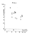
- FIGS. 3 and 4 show the substrate temperatures and layer thicknesses of aluminum (FIG. 3) and silver (FIG. 4) at which diffusely scattering surfaces are obtained when these metals are sputtered in an inert gas atmosphere of 4x10 -3 Torr .
- the layer thickness, measured in nm, is plotted against the substrate temperature, measured in ° C or . in 10- 3 x o K -1 .
- the individual measuring points are drawn as circles, the circular area being blackened to a greater or lesser extent depending on the degree of scattering observed (a completely black circular area represents a completely matt layer).
- FLAD fluorescence-activated displays
Landscapes
- Physics & Mathematics (AREA)
- Nonlinear Science (AREA)
- Mathematical Physics (AREA)
- Chemical & Material Sciences (AREA)
- Crystallography & Structural Chemistry (AREA)
- General Physics & Mathematics (AREA)
- Optics & Photonics (AREA)
- Liquid Crystal (AREA)
- Physical Vapour Deposition (AREA)
- ing And Chemical Polishing (AREA)
- Devices For Indicating Variable Information By Combining Individual Elements (AREA)
Applications Claiming Priority (2)
| Application Number | Priority Date | Filing Date | Title |
|---|---|---|---|
| DE2919572 | 1979-05-15 | ||
| DE19792919572 DE2919572A1 (de) | 1979-05-15 | 1979-05-15 | Passive elektrooptische anzeigevorrichtung und verfahren zur herstellung einer solchen vorrichtung |
Publications (1)
| Publication Number | Publication Date |
|---|---|
| EP0019208A1 true EP0019208A1 (fr) | 1980-11-26 |
Family
ID=6070774
Family Applications (1)
| Application Number | Title | Priority Date | Filing Date |
|---|---|---|---|
| EP80102500A Ceased EP0019208A1 (fr) | 1979-05-15 | 1980-05-07 | Procédé pour la fabrication d'un dispositif d'affichage électro-optique passif |
Country Status (3)
| Country | Link |
|---|---|
| EP (1) | EP0019208A1 (fr) |
| JP (1) | JPS55159476A (fr) |
| DE (1) | DE2919572A1 (fr) |
Cited By (8)
| Publication number | Priority date | Publication date | Assignee | Title |
|---|---|---|---|---|
| FR2472793A1 (fr) * | 1979-12-27 | 1981-07-03 | Suwa Seikosha Kk | Dispositif d'affichage a cristaux liquides |
| EP0044618A3 (fr) * | 1980-06-19 | 1982-06-30 | Itt Industries, Inc. | Dispositifs d'affichage à cristal liquide |
| DE3105063A1 (de) * | 1981-02-12 | 1982-08-19 | Robert Bosch Gmbh, 7000 Stuttgart | Vorrichtung zum anzeigen bzw. sichtbarmachen von informationen, bildern und dgl., mit einem lichtdurchlaessigen informationstraeger und einer beleuchtungseinrichtung |
| US5214522A (en) * | 1990-07-25 | 1993-05-25 | Sony Corporation | Liquid crystal display with back light and conductive diffuser |
| WO1995007495A1 (fr) * | 1993-09-08 | 1995-03-16 | Philips Electronics N.V. | Dispositif d'affichage comprenant un milieu electro-optique |
| WO1995007494A1 (fr) * | 1993-09-08 | 1995-03-16 | Philips Electronics N.V. | Dispositif d'affichage comprenant un milieu electro-optique |
| US5548425A (en) * | 1993-07-21 | 1996-08-20 | Sharp Kabushiki Kaisha | Reflective LCD having a resin-diffuser with dispersed metal oxide particles between a substrate and pixel electrodes or integral with the pixel electrodes |
| EP0823654A3 (fr) * | 1996-08-06 | 1998-11-25 | Canon Kabushiki Kaisha | Dispositif d'affichage réflectif à cristal liquide |
Families Citing this family (2)
| Publication number | Priority date | Publication date | Assignee | Title |
|---|---|---|---|---|
| DE3237323A1 (de) * | 1982-10-08 | 1984-04-12 | Robert Bosch Gmbh, 7000 Stuttgart | Anzeigevorrichtung |
| JPS63290268A (ja) * | 1987-05-20 | 1988-11-28 | Fujitsu Ltd | 薄膜の成長方法 |
Citations (7)
| Publication number | Priority date | Publication date | Assignee | Title |
|---|---|---|---|---|
| US3498818A (en) * | 1968-01-23 | 1970-03-03 | Gen Electric | Method of making highly reflective aluminum films |
| DE2028089A1 (de) * | 1969-06-11 | 1971-01-28 | Kabushiki Kaisha Suwa Seikosha, Tokio | Elektronisches Bildschirmgerat |
| DE2102243A1 (fr) * | 1970-01-19 | 1971-07-29 | Ppg Industries Inc | |
| DE2123828A1 (en) * | 1970-06-05 | 1972-10-19 | Suwa Seikosha Kk | Liquid crystal-contg display device - provided with electrode catalysing recombination of hydrogen and oxygen |
| FR2366659A1 (fr) * | 1976-09-30 | 1978-04-28 | Ibm | Methode de fabrication d'une electrode destinee a un dispositif d'affichage |
| JPS5377497A (en) * | 1976-12-21 | 1978-07-08 | Seiko Epson Corp | Display device |
| DE2813007A1 (de) * | 1977-03-22 | 1978-09-28 | Ebauches Sa | Zweifarbige passive elektrooptische anzeigezelle |
-
1979
- 1979-05-15 DE DE19792919572 patent/DE2919572A1/de not_active Withdrawn
-
1980
- 1980-05-07 EP EP80102500A patent/EP0019208A1/fr not_active Ceased
- 1980-05-14 JP JP6385480A patent/JPS55159476A/ja active Pending
Patent Citations (7)
| Publication number | Priority date | Publication date | Assignee | Title |
|---|---|---|---|---|
| US3498818A (en) * | 1968-01-23 | 1970-03-03 | Gen Electric | Method of making highly reflective aluminum films |
| DE2028089A1 (de) * | 1969-06-11 | 1971-01-28 | Kabushiki Kaisha Suwa Seikosha, Tokio | Elektronisches Bildschirmgerat |
| DE2102243A1 (fr) * | 1970-01-19 | 1971-07-29 | Ppg Industries Inc | |
| DE2123828A1 (en) * | 1970-06-05 | 1972-10-19 | Suwa Seikosha Kk | Liquid crystal-contg display device - provided with electrode catalysing recombination of hydrogen and oxygen |
| FR2366659A1 (fr) * | 1976-09-30 | 1978-04-28 | Ibm | Methode de fabrication d'une electrode destinee a un dispositif d'affichage |
| JPS5377497A (en) * | 1976-12-21 | 1978-07-08 | Seiko Epson Corp | Display device |
| DE2813007A1 (de) * | 1977-03-22 | 1978-09-28 | Ebauches Sa | Zweifarbige passive elektrooptische anzeigezelle |
Non-Patent Citations (2)
| Title |
|---|
| L. HOLLAND: "Vacuum Deposition of Thin Films, 1970, Chapman and Hall Ltd., Seiten 243-245; 444-457 London, G.B. * Seite 245, Absatz 1; Seiten 445, 455; Absatz 4 * * |
| PATENT ABSTRACTS OF JAPAN, Band 2, Nr. 112, 16. September 1978, Seite 6187E78 & JP-A-53 077497 (SUWA SEIKOSHA K.K.) * |
Cited By (9)
| Publication number | Priority date | Publication date | Assignee | Title |
|---|---|---|---|---|
| FR2472793A1 (fr) * | 1979-12-27 | 1981-07-03 | Suwa Seikosha Kk | Dispositif d'affichage a cristaux liquides |
| EP0044618A3 (fr) * | 1980-06-19 | 1982-06-30 | Itt Industries, Inc. | Dispositifs d'affichage à cristal liquide |
| DE3105063A1 (de) * | 1981-02-12 | 1982-08-19 | Robert Bosch Gmbh, 7000 Stuttgart | Vorrichtung zum anzeigen bzw. sichtbarmachen von informationen, bildern und dgl., mit einem lichtdurchlaessigen informationstraeger und einer beleuchtungseinrichtung |
| US5214522A (en) * | 1990-07-25 | 1993-05-25 | Sony Corporation | Liquid crystal display with back light and conductive diffuser |
| US5548425A (en) * | 1993-07-21 | 1996-08-20 | Sharp Kabushiki Kaisha | Reflective LCD having a resin-diffuser with dispersed metal oxide particles between a substrate and pixel electrodes or integral with the pixel electrodes |
| WO1995007495A1 (fr) * | 1993-09-08 | 1995-03-16 | Philips Electronics N.V. | Dispositif d'affichage comprenant un milieu electro-optique |
| WO1995007494A1 (fr) * | 1993-09-08 | 1995-03-16 | Philips Electronics N.V. | Dispositif d'affichage comprenant un milieu electro-optique |
| EP0823654A3 (fr) * | 1996-08-06 | 1998-11-25 | Canon Kabushiki Kaisha | Dispositif d'affichage réflectif à cristal liquide |
| US6292238B1 (en) | 1996-08-06 | 2001-09-18 | Canon Kabushiki Kaisha | Reflection-type liquid crystal apparatus |
Also Published As
| Publication number | Publication date |
|---|---|
| DE2919572A1 (de) | 1980-11-27 |
| JPS55159476A (en) | 1980-12-11 |
Similar Documents
| Publication | Publication Date | Title |
|---|---|---|
| DE69804592T2 (de) | Wärmereflektierender schichtaufbau mit farbkorrektur | |
| DE69419045T2 (de) | Elektrochrome Glasscheibe und seine Anwendung in Fahrzeugen und Bauwesen | |
| DE3941027C2 (de) | Beschichtetes Verglasungsmaterial und Verfahren zu dessen Beschichtung | |
| DE3941046C2 (fr) | ||
| DE69931045T2 (de) | Lichtabsorbierender antireflektierende körper und verfahren zur seiner herstellung | |
| DE2148132C3 (de) | Verfahren zur Herstellung eines dünnen piezoelektrischen Films | |
| DE69123618T2 (de) | Verfahren und Vorrichtung zum Herstellen eines durchsichtigen leitenden Films | |
| DE102004030248B4 (de) | Reflektierender AG-Legierungsfilm für Reflektoren und Reflektor, welcher mit demselben versehen ist | |
| DE3902596C2 (fr) | ||
| DE3506623A1 (de) | Verfahren zum ueberziehen thermisch resistenter substrate und danach hergestellter gegenstand | |
| EP1829835A1 (fr) | Système de couches réfléchissant du royannement infrarouge et la méthode visant sa fabrication | |
| DE2203943B1 (de) | Waermereflexionsscheibe, die gute farbgleichmaessigkeit aufweist, verfahren zu ihrer herstellung sowie ihre verwendung | |
| DE19520843A1 (de) | Scheibe aus durchscheinendem Werkstoff sowie Verfahren zu ihrer Herstellung | |
| DE3329504A1 (de) | Waermewellen-abschirmlamellierung | |
| DE2533364A1 (de) | Beschichtete scheibe | |
| DE19537263C2 (de) | Transparente Wärmeschutzfolie und Verfahren zu deren Herstellung | |
| DE2638097B2 (de) | Verfahren zur Oberflächenbehandlung von Kunststofflinsen | |
| DE2919572A1 (de) | Passive elektrooptische anzeigevorrichtung und verfahren zur herstellung einer solchen vorrichtung | |
| DE2347525C3 (de) | Sonnenschutzglas | |
| DE2063580C2 (de) | Verfahren zum Aufbringen einer transparenten, elektrisch leitfähigen Indiumoxidschicht | |
| EP1581666A2 (fr) | Revetement destine a un substrat plastique | |
| DE4332209A1 (de) | Verfahren zur Herstellung einer Dünnschicht-Elektrolumineszenz-Vorrichtung | |
| DE3903484A1 (de) | Magnetooptischer duennschichtfilm | |
| DE2313730C2 (de) | Verfahren zur Herstellung eines optischen Anzeigeelementes mit einer nematischen flüssigkristallinen Schicht | |
| DE2805884C3 (de) | Flüssigkristall-Anzeigevorrichtung mit einer Fluoreszenzplatte |
Legal Events
| Date | Code | Title | Description |
|---|---|---|---|
| PUAI | Public reference made under article 153(3) epc to a published international application that has entered the european phase |
Free format text: ORIGINAL CODE: 0009012 |
|
| AK | Designated contracting states |
Designated state(s): CH FR GB IT NL |
|
| 17P | Request for examination filed |
Effective date: 19801216 |
|
| STAA | Information on the status of an ep patent application or granted ep patent |
Free format text: STATUS: THE APPLICATION HAS BEEN REFUSED |
|
| 18R | Application refused |
Effective date: 19830630 |
|
| RIN1 | Information on inventor provided before grant (corrected) |
Inventor name: MAYER, GERHARD, DIPL.-PHYS. Inventor name: SEEBACHER, GERHARD, DR. Inventor name: KAUSCHE, HELMOLD, DIPL.-PHYS. Inventor name: KRUEGER, HANS, DIPL.-PHYS. Inventor name: PETERS, WINFRIED, DIPL.-PHYS. |