EP0019355A1 - Structure de transistor - Google Patents
Structure de transistor Download PDFInfo
- Publication number
- EP0019355A1 EP0019355A1 EP80301150A EP80301150A EP0019355A1 EP 0019355 A1 EP0019355 A1 EP 0019355A1 EP 80301150 A EP80301150 A EP 80301150A EP 80301150 A EP80301150 A EP 80301150A EP 0019355 A1 EP0019355 A1 EP 0019355A1
- Authority
- EP
- European Patent Office
- Prior art keywords
- region
- emitter
- regions
- stripe
- transistor structure
- Prior art date
- Legal status (The legal status is an assumption and is not a legal conclusion. Google has not performed a legal analysis and makes no representation as to the accuracy of the status listed.)
- Granted
Links
Images


Classifications
-
- H—ELECTRICITY
- H10—SEMICONDUCTOR DEVICES; ELECTRIC SOLID-STATE DEVICES NOT OTHERWISE PROVIDED FOR
- H10D—INORGANIC ELECTRIC SEMICONDUCTOR DEVICES
- H10D62/00—Semiconductor bodies, or regions thereof, of devices having potential barriers
- H10D62/10—Shapes, relative sizes or dispositions of the regions of the semiconductor bodies; Shapes of the semiconductor bodies
- H10D62/13—Semiconductor regions connected to electrodes carrying current to be rectified, amplified or switched, e.g. source or drain regions
- H10D62/133—Emitter regions of BJTs
-
- H—ELECTRICITY
- H10—SEMICONDUCTOR DEVICES; ELECTRIC SOLID-STATE DEVICES NOT OTHERWISE PROVIDED FOR
- H10D—INORGANIC ELECTRIC SEMICONDUCTOR DEVICES
- H10D48/00—Individual devices not covered by groups H10D1/00 - H10D44/00
- H10D48/30—Devices controlled by electric currents or voltages
- H10D48/32—Devices controlled by only the electric current supplied, or only the electric potential applied, to an electrode which does not carry the current to be rectified, amplified or switched
- H10D48/34—Bipolar devices
- H10D48/345—Bipolar transistors having ohmic electrodes on emitter-like, base-like, and collector-like regions
-
- H—ELECTRICITY
- H10—SEMICONDUCTOR DEVICES; ELECTRIC SOLID-STATE DEVICES NOT OTHERWISE PROVIDED FOR
- H10D—INORGANIC ELECTRIC SEMICONDUCTOR DEVICES
- H10D84/00—Integrated devices formed in or on semiconductor substrates that comprise only semiconducting layers, e.g. on Si wafers or on GaAs-on-Si wafers
- H10D84/101—Integrated devices comprising main components and built-in components, e.g. IGBT having built-in freewheel diode
- H10D84/121—BJTs having built-in components
- H10D84/125—BJTs having built-in components the built-in components being resistive elements, e.g. BJT having a built-in ballasting resistor
Definitions
- This invention relates to transistors.
- Transistors which are capable of operating at high frequencies and at high output powers by connecting in parallel a plurality of transistor units, each for handling low level signals, formed on a semiconductor substrate, have been proposed.
- transistors examples include the overlay type transistor (see U.S. patent No. 3,434,091), and the ring-emitter type transistor (see U.S. patent No. 4,157,561) which have already been developed and put into practical use.
- a base (lead out) electrode and an emitter (lead out) electrode formed on an insulation film of, for example, silicon dioxide (SiOp), formed on the semiconductor substrate, are extensively disposed in the form of the teeth of a comb so that the lead out electrode can connect to each individual isolated transistor unit.
- the insulation film has a pinhole flaw therein or part of the film is missing, the base and emitter are likely to be shorted.
- the width of an electrode or the number of electrodes (or electrode teeth) is increased in order to convey a higher power, probability of short circuiting naturally increases.
- the individual transistor units formed on a semiconductorsubstrate which units together constitute such a transistor, do not always have the same electric characteristics, and when such a transistor operates, it is possible for a particular transistor unit to undergo secondary breakdown due to an excessive load applied thereto as a result of irregularity in the characteristics of the other transistor units.
- a metallic substance such as nichrome (Ni-Cr) for example, or a polycrystalline semiconductor substance such as polycrystalline silicon.
- Such resistor materials may be deposited and laminated in an electrode window provided in the insulating film covering the emitter region of a transistor unit and then one end of the electrode wiring connected to the resistor material (so that the resistor material is between the electrode wiring and the emitter region of the transistor unit).
- the resistor material can be inserted and connected on the insulating film in the midst of electrode wiring, part of which extends up onto the insulating film from an electrode window provided in the insulating film covering the emitter region.
- a diffusion region which is formed in the base region with the same conductivity type as the emitter region, simultaneously with the formation of the emitter region or in a process separate from that by which the emitter region is formed, is used as a stabilizing resistor.
- a diffusion resistor region may be formed in such a way as to come into contact at one end thereof with the emitter region and so that the other end thereof is connected to electrode wiring. Otherwise the diffusion resistor region may be formed in isolation at a distance from the corresponding emitter region with one end of the resistor region connected to the emitter region by way of electrode wiring and the other end lead out by way of further electrode wiring.
- a transistor structure having a collector region of a first conductivity type, and a base region of a second, opposite, conductivity type, characterised in that the structure comprises a further region, of the first conductivity type, formed within the base region, and an additional region, of the second conductivity type, arranged to divide the further region into a plurality of regions of which at least one is an emitter region.
- a transistor structure having a collector region of a first conductivity type, and a base region of a second, opposite, conductivity type, characterised in that the structure comprises a further region, of the first conductivity type, formed within the base region, and an additional region, of the second conductivity type, formed within the further region so as to divide that region into a plurality of emitter regions.
- Embodiments of this invention can provide a transistor structure in which the disadvantages of - transistors having the previously proposed structures mentioned above can be avoided and which can be fabricated with a sufficiently high manufacturing yield.
- a transistor embodying this invention can offer excellent high frequency and high output power characteristics.
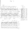
- 11 is a collector region having a structure. for example comprising an N type epitaxial layer formed on an N type semiconductor substrate, for example an N+ type silicon (Si) substrate.
- 12 is a P-type base region formed on a surface of the collector region 11; 13 is an N + type emitter region.formed in the base region 12 (see (c) particularly).
- Each emitter region 13 is in the form of a strip. Together, a number of regions 13 may be likened to the teeth of a comb 14 is a P type isolation region formed in the emitter region 13; 15 is a P type base contact region.
- the base contact region 15, as best seen in (a) is formed in the base region 12, and extends along region 12 between emitter regions 13 and parallel thereto.
- 16a and 16b are emitter lead-out electrodes (seen in section in (c) and indicated by chain lines in (a). In (b) only 16a can be seen in section). The lead-out electrodes 16a and 16b extend over respective stripe or strip-like emitter regions 13.
- the lead out electrode 17a is a base lead-out electrode (seenin section in (c) and indicated by a chain line in (a)).
- the lead out electrode 17a extends over the base contact region 15.
- 18 is an insulating film covering a semiconductor substrate surface.
- 19-a, 19-b, 19-c ... are emitter lead-out electrode connecting windows which are formed in the insulating film18.
- 20-a, 20-b, 20-c, ... are base lead-out electrode connecting windows formed in the insulating film 18.
- 21 is a collector electrode.
- a transistor structure embodying this invention is such that the stripe or strip-like emitter region 13 is divided into a number of small active emitter regions 13-a, 13-b, ... by the-isolation regions 14 which, as best seen in (a), are disposed so as to lie across the emitter region 13 in directions orthogonal to the elongate direction (the stripe direction) of region 13.
- Each small active emitter region 13-a, 13-b, etc is generally rectangular in shape.
- the isolation regions 14 do not divide the stripeor strip-like emitter region 13 into small active emitter regions by a process such that they contact the base region 12 by extending completely across the stripe emitter region 13 and/or by extending completely through the depth of emitter region 13.
- the isolation regions 14 are disposed in the stripe emitter region 13 in the form of lands so that the cross section of the emitter region 13 is reduced to the sides (upper and/or lower sides as seen in (a) and (c)) of the isolation regions 14 considered along the direction of the emitter region strip.
- the cross section of the emitter region is also reduced in depth, under the isolation region, as best seen in (c).
- the emitter region 13 is divided into small emitter regions 13-a, 13-b, ... due to resistance generated as a result of the reduction of cross section thereof by the isolation regions.
- the respective isolated small emitter regions 13-a, 13-b, ... respectively provide transistor operation over emitter-base juction areas near to the respective adjacent base contact regions 15.
- a small emitter region, the base region which contacts the small emitter region and the collector region under the base region form a transistor unit.
- a single stripe emitter region 13 is so structured as to provide a plurality of small emitter regions which are connected in parallel with one another by an emitter lead-out electrode.
- a plurality of stripe emitter regions can themselves be connected in parallel, and a transistor structure embodying this invention can have a structure which is suited for giving high frequency and high output power characteristics.
- a plurality of small emitter regions are provided in the form of a matrix of emitter regions.
- the emitter lead-out electrodes 16 which are disposed on and extended over stripe emitter regions 13 and which connect in parallel the pluralities of small emitter regions formed in the stripe emitter regions via lead-out electrode connecting windows are such that they connect the small emitter regions in parallel without being disposed on the base region.
- the emitter lead-out electrodes 16 can be connected through the pinholes to the isolation regions 14, but not to the base region and short circuits can therefore occur only between the isolation regions 14 and the emitter region and cannot lead to a short between the emitter region and base region since the isolation regions 14 are isolated and insulated from the base region by the emitter region itself and are set in a floating condition from the electrical viewpoint when in operation.
- problems of reduction in the manufacturing yield and in reliability due to pinholes in the insulating film under an emitter lead-out electrode can be avoided.
- an emitter lead-out electrode can be formed to extend over almost all of the width of a single stripe emitter region, offering an increase in effective electrode cross section, and this transistor structure can effectively provide for a high output power by increasing the number of transistor units formed in a stripe emitter region.
- the isolation regions 14 can be formed simultaneously with stabilizing resistor regions and/or base contact regions by a diffusion method as will be explained later, the number of manufacturing steps needed to form the transistor structure is not increased.
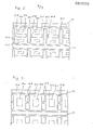
- Figure 2 and Figure 3 illustrate further transistor structures embodying this invention in which, in comparison with Fig. 1, the forms of isolation regions disposed within a stripe emitter region differs from that of the transistor structure of Fig. 1.
- stripe emitter region 13 is isolated, separated, into a plurality of small emitter regions 13-a, 13-b, ... by isolation regions 14-1 disposed in directions orthogonal to the stripe direction and by isolation regions 14-11 disposed in directions parallel to the stripe direction.
- the small emitter regions have a rectangular shape.
- the region 15 is a P type base contact region as already explained with reference to Fig. 1.
- the stripe emitter region 13 is isolated into a plurality of small emitter regions 13-a, 13-b, ... by isolation regions 14-III which are disposed in directions orthogonal to the stripe direction. As compared with Fig. 1 it is as if each isolation region has been separated into two regions. Each of the isolated small emitter regions allows the disposition of an emitter lead-out electrode connecting window 19-a, 19-b, ... on the insulating film covering the surface of the region.
- the small emitter regions 13a, 13b, ... in the stripe emitter region 13 are isolated by cross-section reduction to the sides of the isolation regions 14-III and also below the isolation regions 14-III (i.e. reduced in depth).
- the region 15 is the P type base contact region.
- Figure 4 and Figure 5 illustrate the structures of transistors embodying the present invention having forms generally similar to those of Figs. 1 to 3 but wherein stabilizing resistors are inserted between the small emitter regions formed in a stripe emitter region and the relevant emitter lead-out electrode.
- stabilizing resistors are inserted between the small emitter regions formed in a stripe emitter region and the relevant emitter lead-out electrode.
- isolation regions are inserted in accordance with the structure shown in Fig. 1 above.
- emitter lead-out electrodes 16 are disposed to extend generally along the center lines of the stripe emitter regions 13 (one is shown in Fig. 4) in the direction of the stripe, and electrically conductive, metallic wiring (or electrode) layers 41 are disposed in parallel to the emitter lead-out electrodes 16 on opposite sides of the emitter lead-out electrode 16, on each of the small emitter regions 13-a, 13-b etc.
- Metallic wiring layers 41 are connected to a small emitter region (for example, 13-a) via connecting windows 42-a, 42-b provided in the insulating film over the emitter region (see film 18 in Fig.
- a stabilizing resistor is formed by an impurity injection region having a conductivity type opposite to that of the emitter region as mentioned above in a structure such that the i stabilizing resistor is inserted between the emitter lead-out electrode 16 and a small emitter region
- application of such structure into a stripe emitter region having a structure as shown in Fig. 2 is difficult to realize because of the existence of ) the isolation region 14-11.
- a stabilizing resistor consisting of a resistor material, for example a polycrystalline semiconductor layer 5 or a metallic layer (of nichrome for example) between the emitter lead-out electrode and metallic wiring layer which connects the stabilizing resistor to the small emitter region in order to connect the lead-out electrode and the metallic wiring layer in the form of the bridge on the insulating film on which the emitter lead-out electrode and the metallic wiring layer are themselves disposed.
- a stabilizing resistor consisting of a resistor material, for example a polycrystalline semiconductor layer 5 or a metallic layer (of nichrome for example) between the emitter lead-out electrode and metallic wiring layer which connects the stabilizing resistor to the small emitter region in order to connect the lead-out electrode and the metallic wiring layer in the form of the bridge on the insulating film on which the emitter lead-out electrode and the metallic wiring layer are themselves disposed.
- stabilizing resistors consisting of polycrystalline semiconductor layers or metallic layers can also be used.
- metallic wiring (or electrode) layers 51 are disposed on the small emitter regions generally along the center line thereof, in the direction of the stripe emitter region 13, and emitter lead-out electrodes 16,', 16" are disposed in the stripe direction to opposite sides of the metallic wiring layers 51.
- two emitter lead-out electrodes cover one stripe emitter region.
- Metallic wiring layer 51 is connected to a small emitter region (13-a, for example) via connecting windows 52-a, 52-b provided in the insulating film over the emitter region, while the metallic wiring layers 51 and emitter lead-out electrodes 16', 16" connected to one another by a P type stabilizing resistorregion 53 as shown in the Figure.
- the stabilizing resistor region 53 and the emitter lead-out electrodes 16', 16" are connected via connecting windows 54-a, 54-b, while the stabilizing resistor region 53 and the metallic wiring layer 51 are connected via connecting window 52-c.
- an emitter current flows to a stabilizing resistor and an emitter lead-out electrode from both ends of the metallic wiring layer disposed generally centrally of the small emitter region concerned, at least the emitter-base junction areas near the base contact regions 15 in a small emitter region operate equally.
- a pair of emitter lead-out electrodes are disposed in parallel over a small emitter region resulting in an increase of the effective cross section area. Therefore, a structure as shown in Fig. 5 can be very effective for obtaining a higher output power by connecting in parallel the plurality of small emitter regions.
- the stabilizing resistor can be composed of a polycrystalline semiconductor layer or a metallic layer of nichrome as is explained previously.
- one of the two emitter lead-out electrodes 16', 16" and a stabilizing resistor part connected thereto may be omitted in order to provide a structure design such that a small capacity of current flows through the small emitter regions.
- a transistor structure which can process a high frequency signal and offer a higher output power can be structured by separating a stripe or strip-like emitter region into small emitter regions by disposition of (isolation) regions having an opposite conductivity type into the emitter region, and by connecting said small emitter regions in parallel directly or via stabilizing resistors using emitter lead-out electrodes disposed on the stripe emitter region.
- At least the emitter lead-out electrodes connect in parallel the small emitter regions disposed and mutually isolated within the stripe emitter region.
- the isolation regions are put in a floating condition (in use) and lie within the emitter region, a short between emitter and base does not occur even when pinholes exist in the insulating film separating emitter region and emitter lead out electrodes, thereby preventing reduction in manufacturing yield and deterioration of reliability due to the presence of such shorts.
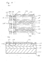
- FIG. 6 illustrates another transistor structure embodying.this invention.
- (a) is a plan view of the structure
- (b) is a cross-sectional view taken along the line X-X' of (a)
- (c) is a cross-sectional view taken along the line Y-Y' of (a).
- 61 is a collector region having a structure for example comprising an N type epitaxial layer formed on an N type semiconductor substrate, for example, a silicon substrate.
- 62 is a P type base region formed on the collector region 61.
- 63 is an N type emitter region which is a stripe or strip-like formed within the base region 62.
- 64 is a P type stabilizing resistor region formed within said emitter region 63.
- 65 is a P + type base contact region. The base contact region 65 is formed in the base region 62 and extends alongside the stripe emitter region 63.
- 66 is a metallic wiring (or electrode) layer which connects a stabilizing resistor region 64 and an emitter region 63; 67-a, 67-b are emitter lead-out electrodes; and 68-a, 68-b are base lead-out electrodes.
- 69 is an insulating film covering a semiconductor substrate surface; 70-a, 70-b and 70-c are windows through which metallic electrode layers 66 formed on the insulating film 69 are connected to stabilizing resistor regions 64 and emitter regions 63; 71-a, 71-b are emitter lead-out electrode windows formed through the insulating film 69; 72-a, 72-b, ... are base lead-out electrode connecting windows formed through the insulating film 69 and.73 is the collector electrode.
- a transistor having a structure as illustrated in Figure 6 has a stripe emitter region 63 which is separated into a plurality of isolated small active emitter regions by the P type regions 64 which are structured to act as stabilizing resistors and are disposed in the emitter region selectively and extend in directions orthogonally crossing the emitter stripe direction.
- the isolation regions and stabilizing resistor regions which have been provided separately in the previous embodiments are integrated into one structure and the stripe emitter region 63 is isolated into several small emitter regions by means of the stabilizing resistor regions 64.
- the stabilizing resistor regions 64 are disposed in the form of lands in the stripe emitter region 63 as best seen in (c) and the cross section of the emitter region is reduced to the sides of the regions 64 (as seen in (a) and (c)) and is reduced in depth below the stabilizing resistor regions 64, going along a stripe emitter region in the stripe direction and thereby the stripe emitter region 63 is divided into a plurality of small isolated emitter regions due to increase of resistance value in the emitter region where the cross section thereof is reduced or constricted.
- the separate small emitter regions respectively operate at the emitter-base junction areas near the adjacent base contact regions 65.
- a single stripe emitter region 63 is effectively composed of plurality of small emitter regions connected in parallel by the emitter lead-out electrodes.
- a transistor having a structure as illustrated in Fig. 6 is suitable for high frequency signal operation and higher output power operation as in the case of the previous embodiments when stripe emitter regions are themselves connected in parallel.
- the emitter lead-out electrodes 67 connect in parallel the small emitter regions without being disposed on the base region. Therefore, even if an emitter lead-out electrode 67 is inadvertently connected to the stabilizing resistor region 64 due to existence of pinholes in the insulating film separating electrode 67 and region 64, short circuits can occur only between the stabilizing resistor region 64 and the emitter region and cannot lead to a short between the emitter region and the base region since a stabilizing resistor region 64 is isolated and insulated from the base region by the emitter region itself.and is put in a floating condition from the A electrical viewpoint.
- the stabilizing resistor region 64 can be formed by diffusion simultaneously with formation of the base contact region, whereby the number of manufacturing steps required is not increased.
- a stabilizing resistor region also functions as an isolation region, and therefore the integration density of a transistor unit so structured can be increased at least as compared with units structured in accordance with Fig. 4 or Fig. 5..
- the metallic electrode layers 66 and emitter lead-out electrodes 67 as shown in Fig. 6 may be alternatively formed as illustrated in Fig. 4. That is, one emitter lead-out electrode 67 may be disposed along the center line of an emitter stripe extending in the stripe direction, with metallic electrode layers 66 disposed in parallel to the emitter lead-out electrode 67, on either side thereof.
- the small emitter regions are defined in a stripe emitter region and the isolation regions and/or stabilizing resistor regions are disposed selectively to define those small emitter regions.
- This invention can also be applied in a transistor structure as follows.
- adjacent ends of the respective stripe emitter regions may be integrated by means of a region having a conductivity type the same as that of said emitter regions to provide for such parallel connection.
- a lead wire connecting part, for external lead-out of the transistor, a so called bonding pad, can be disposed on the region which provides the parallel connection.
- Such a bonding pad arrangement is employed to eliminate the possibility of shorts between the emitter electrodes and the base regions under the insulating film arising as a result of the existence of pinholes in the insulating film under the bonding pad or as a result of cracks generated when connecting lead wires.
- the region having. a conductivity type the same as that of the emitter regions for integrating the emitter regions in the area under the bonding pad can cause generation of a parasitic transistor unit in the region under the bonding pad and also result in deterioration of breakdown voltage of the transistor.
- a structure as illustrated in Fig. 7 (a) can be used.
- stripe emitter regions are integrated with a region 101 which lies under a bonding pad (not shown).
- Fig. 7(a) stripe emitter regions are integrated with a region 101 which lies under a bonding pad (not shown).
- Fig. 7(a) stripe emitter regions are integrated with a region 101 which lies under a bonding pad (not shown).
- Fig. 7(a) stripe emitter regions are integrated with a region 101 which lies under a bonding pad (not shown).
- the connection areas between each stripe emitter region 102 and region 101 isolation regions 103 having a conductivity type opposite to that of the emitter regions are disposed.
- Each stripe emitter region is thus permitted to operate independently and the region 101 under the bonding pad becomes inactive electrically, thus suppressing and preventing parasitic transistor operation.
- FIG. 7(b) a - structure is shown in which stripe emitter regions 102 extend from either side of an integrating region 101 (over which a bonding pad is formed).
- a single isolation region 103 having opposite conductivity type to that of the emitter region is formed to take up almost all the area of the region 101 including areas adjacent to the areas of the region 101 which connect to the stripe emitter regions.
- Generation of parasitic transistor operation due to pinholes or cracks in the insulating film and shorts between the emitter electrddeand base region, can beprevented reliably by this structure when the bonding pad is formed on the region 101 over the insulating film.
- isolation regions in the nodes connecting a region under the bonding pad to stripe emitter regions of source can be adopted to the embodiments of this invention shown in Fig. 1 to Fig. 6 of course.
- stripe form small emitter regions can be provided.
- a stabilizing resistor region can be adopted as an isolation region which isolates a stripe emitter region from a region under a bonding pad which connects in parallel a plurality of such stripe emitter regions.
- Such a structure provides for the simultaneous separation of the stripe emitter regions and insertion of stabilizing resistor regions.
- Figure 8 illustrates such a transistor structure.
- (a) is a plan view of the transistor structure and
- (b) is a cross-sectional view taken along the line X-X' in (a).
- 111 is a collector region having a structure such that an N type epitaxial layer is formed, for example, on an N type semiconductor substrate; 112 is a P type base region formed on the collector region; 113 is an N + type stripe emitter region formed in the base region 112; 113' is an N type region, under a bonding pad, which connects in parallel a number of emitter regions 113; 114 is a P type stabilizing resistor region; and-115 is a P type base contact region.
- 116 is an emitter electrode
- 117 is an emitter lead-out electrode forming a bonding pad
- 118 is a base lead-out electrode.
- 119 is an insulating film covering the semiconductor substrate surface; 120 is an emitter electrode connecting window formed in the insulating film 119; 121 is a connecting window for connecting the emitter electrode 116 to the stabilizing resistor region 114, which window is formed in the insulating film 119; 122 is an emitter lead out electrode connecting window formed in the insulating film 119; and 123 is a base lead-out electrode connecting window formed in the insulating film 119.
- 124 is a collector electrode.
- a-stripe emitter region 113 is connected to the emitter lead-out electrode 117 via a stabilizing resistor region and is isolated from region 113' under the bonding pad by that stabilizing resistor region.
- each stripe emitter region 113 can operate individually without causing a concentration of a current, and the region 113' under the bonding pad is rendered inactive electrically. Thereby, the transistor structure of Figure 8 can therefore operate without deterioration - in the current amplification factor.
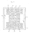
- Figure 9 is a plan view of a transistor chip accommodating transistor unit structures as illustrated in Fig. 6.
- 151 is, for example a part of a transistor chip; 152 is an individual transistor unit.
- 153 is an emitter lead-out electrode; 154 is an emitter electrode terminal pad; 155 is a base lead-out electrode; 156 is a base electrode terminal pad; and 157 is a metallic wiring (or electrode) layer.
- a base contact region is indicated to have an elongate rectangular shape and to be disposed alongside the full length of a stripe emitter region.
- a base contact region can take the shape of land (e.g. that region need not extend the full length of a stripe emitter region) and a base lead-out electrode connecting window can alternatively be formed along the full length of the base contact region.
- a collector region constituted by an N type layer on an N type semiconductor substrate can be formed by epitaxial growth of an N type layer on an N type semiconductor substrate by a conventional method, or by a process in which a high concentration of a donor impurity such as phosphorus (P) is injected from both sides of the N type semiconductor substrate in order to form N type layers on both sides of the substrate, whereafter one of the N type layers is removed.
- a donor impurity such as phosphorus (P)
- a P type base region can be formed by a conventional complete diffusion method or by-a method involving selective diffusion of an acceptor impurity such as boron (B) for example.
- B acceptor impurity
- a transistor if a transistor is to be used for handling a high voltage, it should have a so-called mesa structure wherein the base-collector (BC) junction appears in a side of a piece of semiconductor chip.
- the transistor if the transistor is to be used for handling a comparatively low voltage, it should have a so-called planar structure wherein the BC junction terminates at the surface of the collector region.
- the base contact region can be formed selective injection of acceptor impurity, as in the case of the base region, but with a higher concentration of impurity than that injected into the base region by the diffusion method.
- the N type emitter region can be formed by selectively injecting a high concentration of donor impurity such as arsenic (As), phosphorus (P) into the base region by a diffusion method.
- donor impurity such as arsenic (As), phosphorus (P)
- the P type isolation regions and the P type stabilizing resistor regions can be formed by selectively injecting a high concentration of acceptor impurity into the emitter region by a diffusion method.
- the base contact region can be formed simultaneously with the diffusion of the isolation regions and/or the stabilizing resistor regions which are specified as having a diffusion depth.
- silicon dioxide Si0 2
- Si3N4 silicon nitride
- PSG phosphor- silicate glass
- the emitter lead-out electrode, base lead-out electrode and metallic electrode layers can be formed, for example, by vacuum evaporation of aluminium (Al) and photo-etching, and electrical connection to the various regions formed in the substrate (e.g. base contact region etc) can be provided through electrode windows which are formed in the insulating film by photo-etching.
- the emitter region may be formed to an unnecessary depth due to the so-called emitter-dip effect. This can result in reduced emitter-base breakdown voltage and reduced emitter-collector breakdown voltage, and in addition it can become difficult to obtain a sufficient current amplification factor in some cases.
- the following measures can be taken.
- the emitter diffusion is carried out so that emitter region areas shallower than emitter region areas formed simultaneously in a peripheral flat area (around an extruded, projecting or mesa area) are formed in the areas under the extruded areas.
- the emitter dip level reached when the isolation regions and stabilizing resistor regions are formed in the extruded area is thus taken into account in advance and the emitter dip effect is cancelled and compensated.
- embodiments of this invention use a transistor structure in which a base region having a conductivity type opposite to that of a collector is formed on the collector and an emitter region having a conductivity type the same as the collector is formed in the base region.
- the emitter lead-out electrodes are disposed so as to extend over the emitter region and connect in parallel isolated small emitter regions via lead-out .electrode connecting windows, thereby the emitter lead-out electrodes are capable of connecting in parallel the small emitter regions without having to be disposed over the base region.
- an emitter lead-out electrode can be formed to cover almost the entire area of a single emttterregion, increasing the effective cross section.
- Such a structure can be very effective for handling high output power by increasing the number of transistor units formed in a stripe emitter region.
- the isolation regions can be formed by a diffusion method simultaneously with the formation of stabilizing resistor regions and/or base contact .region, the number of manufacturing steps needed is not increased.
- embodiments of this invention can offer a transistor having excellent electrical characteristics without reduction in manufacturing yield but requiring only the same number or fewer manufacturing steps by improving the isolation structure of each transistor unit, the structure forming stabilizing resistor regions in the transistor units, the structure for leading out emitter lead-out electrodes; and moreover the structure for forming the base contact region.
- the shape of the stabilizing resistor regions is not limited to a shape having a constricted part. as in the case of the illustrated embodiments. It is of course possible to have other shapes having no constricted parts so long as the desired resistance values can be obtained.
- transistors embodying this invention have a structure suitable for high frequency and high output power operation.
- An emitter region of one conductivity type is formed in a base region of the opposite conductivity type which base region is in contact with a collector region also of the one conductivity type.
- the emitter region is divided into plurality of active emitter regions by isolation regions of the opposite conductivity type which are formed in the emitter region and these active emitter regions are connected in parallel by an emitter electrode or lead-but electrode.
- Stabilizing e resistor regions constitutlby regions of the opposite conductivity type, or by other resistor material may be inserted and connected between active emitter regions and the emitter electrode or lead-out electrode.
Landscapes
- Bipolar Transistors (AREA)
Applications Claiming Priority (2)
| Application Number | Priority Date | Filing Date | Title |
|---|---|---|---|
| JP4396779A JPS55138273A (en) | 1979-04-11 | 1979-04-11 | Transistor |
| JP43967/79 | 1979-04-11 |
Publications (2)
| Publication Number | Publication Date |
|---|---|
| EP0019355A1 true EP0019355A1 (fr) | 1980-11-26 |
| EP0019355B1 EP0019355B1 (fr) | 1984-03-28 |
Family
ID=12678471
Family Applications (1)
| Application Number | Title | Priority Date | Filing Date |
|---|---|---|---|
| EP80301150A Expired EP0019355B1 (fr) | 1979-04-11 | 1980-04-10 | Structure de transistor |
Country Status (4)
| Country | Link |
|---|---|
| US (1) | US4370670A (fr) |
| EP (1) | EP0019355B1 (fr) |
| JP (1) | JPS55138273A (fr) |
| DE (1) | DE3067237D1 (fr) |
Cited By (7)
| Publication number | Priority date | Publication date | Assignee | Title |
|---|---|---|---|---|
| EP0054434B1 (fr) * | 1980-12-15 | 1986-05-28 | Fujitsu Limited | Dispositif à semiconducteurs |
| EP0098209B1 (fr) * | 1982-06-25 | 1986-09-17 | Thomson-Csf | Transistor de commutation de puissance à structure digitée |
| GB2175441A (en) * | 1985-05-03 | 1986-11-26 | Texas Instruments Ltd | Power bipolar transistor |
| US4639757A (en) * | 1980-12-12 | 1987-01-27 | Hitachi, Ltd. | Power transistor structure having an emitter ballast resistance |
| DE3802821A1 (de) * | 1988-01-30 | 1989-08-03 | Bosch Gmbh Robert | Leistungstransistor |
| DE3802767A1 (de) * | 1988-01-30 | 1989-08-10 | Bosch Gmbh Robert | Elektronisches geraet |
| WO1991003077A1 (fr) * | 1989-08-16 | 1991-03-07 | Robert Bosch Gmbh | Puce de grande capacite realisee en technologie planaire et equipee de transistors de commutation |
Families Citing this family (15)
| Publication number | Priority date | Publication date | Assignee | Title |
|---|---|---|---|---|
| DE3017750C2 (de) * | 1980-05-09 | 1985-03-07 | Philips Patentverwaltung Gmbh, 2000 Hamburg | Halbleiterbauelement vom Planar-Epitaxial-Typ mit mindestens einem bipolaren Leistungstransistor |
| JPS59135651U (ja) * | 1983-03-02 | 1984-09-10 | 三洋電機株式会社 | トランジスタ |
| JPS59135652U (ja) * | 1983-03-02 | 1984-09-10 | 三洋電機株式会社 | トランジスタ |
| DE3443771C2 (de) * | 1984-11-30 | 1994-05-26 | Bosch Gmbh Robert | Halbleiteranordnung mit Metallisierung |
| US4656496A (en) * | 1985-02-04 | 1987-04-07 | National Semiconductor Corporation | Power transistor emitter ballasting |
| US4812890A (en) * | 1985-11-19 | 1989-03-14 | Thompson-Csf Components Corporation | Bipolar microwave integratable transistor |
| FR2615326B1 (fr) * | 1987-05-15 | 1990-08-31 | Fuji Electric Co Ltd | Dispositif a semi-conducteurs du type multi-emetteur |
| US5298785A (en) * | 1987-05-15 | 1994-03-29 | Fuji Electric Co., Ltd. | Semiconductor device |
| US4901120A (en) * | 1987-06-10 | 1990-02-13 | Unitrode Corporation | Structure for fast-recovery bipolar devices |
| US5204735A (en) * | 1988-04-21 | 1993-04-20 | Kabushiki Kaisha Toshiba | High-frequency semiconductor device having emitter stabilizing resistor and method of manufacturing the same |
| US5488252A (en) * | 1994-08-16 | 1996-01-30 | Telefonaktiebolaget L M Erricsson | Layout for radio frequency power transistors |
| US5859465A (en) * | 1996-10-15 | 1999-01-12 | International Rectifier Corporation | High voltage power schottky with aluminum barrier metal spaced from first diffused ring |
| DE19734985B4 (de) * | 1997-08-13 | 2010-02-11 | Robert Bosch Gmbh | Transistorbauelement |
| JP2003045882A (ja) * | 2001-07-27 | 2003-02-14 | Nec Corp | 半導体装置及びその設計方法 |
| USD848384S1 (en) * | 2017-08-17 | 2019-05-14 | Epistar Corporation | Transistor |
Citations (7)
| Publication number | Priority date | Publication date | Assignee | Title |
|---|---|---|---|---|
| US2314582A (en) * | 1941-02-13 | 1943-03-23 | Gerich Valentine | Two-way driftpin, swaging and aligning tool |
| DE2241306A1 (de) * | 1971-08-30 | 1973-03-08 | Rca Corp | Transistor mit veraenderlichem ballastwiderstand |
| DE2332144A1 (de) * | 1973-06-25 | 1975-01-16 | Licentia Gmbh | Transistor |
| FR2314582A1 (fr) * | 1975-06-10 | 1977-01-07 | Ates Componenti Elettron | Dispositif a semi-conducteur du type planaire epitaxial |
| US4038680A (en) * | 1972-12-29 | 1977-07-26 | Sony Corporation | Semiconductor integrated circuit device |
| FR2374743A1 (fr) * | 1976-12-20 | 1978-07-13 | Radiotechnique Compelec | Transistor multicouche a emetteur compose |
| NL7901855A (nl) * | 1978-03-10 | 1979-09-12 | Fujitsu Ltd | Transistor. |
Family Cites Families (4)
| Publication number | Priority date | Publication date | Assignee | Title |
|---|---|---|---|---|
| US3462658A (en) * | 1965-10-12 | 1969-08-19 | Bendix Corp | Multi-emitter semiconductor device |
| JPS5139075B1 (fr) * | 1966-09-22 | 1976-10-26 | ||
| US3667008A (en) * | 1970-10-29 | 1972-05-30 | Rca Corp | Semiconductor device employing two-metal contact and polycrystalline isolation means |
| US3665266A (en) * | 1970-12-10 | 1972-05-23 | Motorola Inc | Low saturation resistance,low offset voltage,monolithic analog switch |
-
1979
- 1979-04-11 JP JP4396779A patent/JPS55138273A/ja active Granted
-
1980
- 1980-04-07 US US06/138,111 patent/US4370670A/en not_active Expired - Lifetime
- 1980-04-10 EP EP80301150A patent/EP0019355B1/fr not_active Expired
- 1980-04-10 DE DE8080301150T patent/DE3067237D1/de not_active Expired
Patent Citations (8)
| Publication number | Priority date | Publication date | Assignee | Title |
|---|---|---|---|---|
| US2314582A (en) * | 1941-02-13 | 1943-03-23 | Gerich Valentine | Two-way driftpin, swaging and aligning tool |
| DE2241306A1 (de) * | 1971-08-30 | 1973-03-08 | Rca Corp | Transistor mit veraenderlichem ballastwiderstand |
| US4038680A (en) * | 1972-12-29 | 1977-07-26 | Sony Corporation | Semiconductor integrated circuit device |
| DE2332144A1 (de) * | 1973-06-25 | 1975-01-16 | Licentia Gmbh | Transistor |
| FR2314582A1 (fr) * | 1975-06-10 | 1977-01-07 | Ates Componenti Elettron | Dispositif a semi-conducteur du type planaire epitaxial |
| FR2374743A1 (fr) * | 1976-12-20 | 1978-07-13 | Radiotechnique Compelec | Transistor multicouche a emetteur compose |
| NL7901855A (nl) * | 1978-03-10 | 1979-09-12 | Fujitsu Ltd | Transistor. |
| WO1979000736A1 (fr) * | 1978-03-10 | 1979-10-04 | Fujitsu Ltd | Transistors |
Non-Patent Citations (3)
| Title |
|---|
| ELECTRONIC DESIGN, Vol. 27, No. 7, March 29, 1979 Rochelle Park US D. BAUGHER: "To Pick the right power semiconductor, understand device processing methods", pages 142-147 * Figure 1 * * |
| International publication WO 79/ 00736 (FUJITSU) * Abstract; figures 1-3, 5-17 * & NL - A - 79 01855. * |
| SOLID STATE ELECTRONICS, Vol. 13, July 1970, London GB D. KASPERKOVITZ: "The hook-emitter transistor: a proposed amplifier with high gain-bandwith product" pages 1025-1031 * Abstract, page 1027, column 2, last paragraph - page 1030, column 2, paragraph 2; figure 5b * * |
Cited By (10)
| Publication number | Priority date | Publication date | Assignee | Title |
|---|---|---|---|---|
| US4639757A (en) * | 1980-12-12 | 1987-01-27 | Hitachi, Ltd. | Power transistor structure having an emitter ballast resistance |
| EP0054434B1 (fr) * | 1980-12-15 | 1986-05-28 | Fujitsu Limited | Dispositif à semiconducteurs |
| EP0098209B1 (fr) * | 1982-06-25 | 1986-09-17 | Thomson-Csf | Transistor de commutation de puissance à structure digitée |
| GB2175441A (en) * | 1985-05-03 | 1986-11-26 | Texas Instruments Ltd | Power bipolar transistor |
| GB2175441B (en) * | 1985-05-03 | 1989-05-10 | Texas Instruments Ltd | Power bipolar transistor |
| DE3802821A1 (de) * | 1988-01-30 | 1989-08-03 | Bosch Gmbh Robert | Leistungstransistor |
| DE3802767A1 (de) * | 1988-01-30 | 1989-08-10 | Bosch Gmbh Robert | Elektronisches geraet |
| WO1989007340A1 (fr) * | 1988-01-30 | 1989-08-10 | Robert Bosch Gmbh | Appareil electronique |
| US5068703A (en) * | 1988-01-30 | 1991-11-26 | Robert Bosch Gmbh | Electronic circuit device |
| WO1991003077A1 (fr) * | 1989-08-16 | 1991-03-07 | Robert Bosch Gmbh | Puce de grande capacite realisee en technologie planaire et equipee de transistors de commutation |
Also Published As
| Publication number | Publication date |
|---|---|
| DE3067237D1 (en) | 1984-05-03 |
| US4370670A (en) | 1983-01-25 |
| JPS55138273A (en) | 1980-10-28 |
| JPS572185B2 (fr) | 1982-01-14 |
| EP0019355B1 (fr) | 1984-03-28 |
Similar Documents
| Publication | Publication Date | Title |
|---|---|---|
| EP0019355A1 (fr) | Structure de transistor | |
| US4038680A (en) | Semiconductor integrated circuit device | |
| US3411051A (en) | Transistor with an isolated region having a p-n junction extending from the isolation wall to a surface | |
| US3858237A (en) | Semiconductor integrated circuit isolated through dielectric material | |
| US3902188A (en) | High frequency transistor | |
| US4835588A (en) | Transistor | |
| JPH07142621A (ja) | 垂直バイポーラトランジスタおよび垂直mosfetトランジスタの集積モノリシック装置 | |
| US3746949A (en) | Semiconductor device | |
| JPH0793313B2 (ja) | ラテラル トランジスタを有する集積回路 | |
| US3755722A (en) | Resistor isolation for double mesa transistors | |
| EP0117867A1 (fr) | Arrangement de semi-conducteur | |
| US3879745A (en) | Semiconductor device | |
| EP0054303B1 (fr) | Semiconducteur à circuit intégré | |
| US4125853A (en) | Integrated circuit transistor | |
| EP0024923B1 (fr) | Structure de transistor | |
| JPS6231832B2 (fr) | ||
| KR830001956B1 (ko) | 트랜지스터 | |
| JPS6366948A (ja) | プログラマブルボンデイングパツド | |
| US4097888A (en) | High density collector-up structure | |
| KR920003703B1 (ko) | 반도체 장치 | |
| JP2518929B2 (ja) | バイポ―ラ型半導体集積回路 | |
| JPS6244430B2 (fr) | ||
| JP2518413B2 (ja) | 半導体集積回路 | |
| JPS6348189B2 (fr) | ||
| JP2665820B2 (ja) | ラテラルトランジスタ |
Legal Events
| Date | Code | Title | Description |
|---|---|---|---|
| PUAI | Public reference made under article 153(3) epc to a published international application that has entered the european phase |
Free format text: ORIGINAL CODE: 0009012 |
|
| AK | Designated contracting states |
Designated state(s): DE FR GB NL |
|
| 17P | Request for examination filed |
Effective date: 19810211 |
|
| GRAA | (expected) grant |
Free format text: ORIGINAL CODE: 0009210 |
|
| AK | Designated contracting states |
Designated state(s): DE FR GB NL |
|
| REF | Corresponds to: |
Ref document number: 3067237 Country of ref document: DE Date of ref document: 19840503 |
|
| ET | Fr: translation filed | ||
| PLBE | No opposition filed within time limit |
Free format text: ORIGINAL CODE: 0009261 |
|
| STAA | Information on the status of an ep patent application or granted ep patent |
Free format text: STATUS: NO OPPOSITION FILED WITHIN TIME LIMIT |
|
| 26N | No opposition filed | ||
| PGFP | Annual fee paid to national office [announced via postgrant information from national office to epo] |
Ref country code: GB Payment date: 19920204 Year of fee payment: 13 |
|
| PGFP | Annual fee paid to national office [announced via postgrant information from national office to epo] |
Ref country code: FR Payment date: 19920429 Year of fee payment: 13 |
|
| PGFP | Annual fee paid to national office [announced via postgrant information from national office to epo] |
Ref country code: NL Payment date: 19920430 Year of fee payment: 13 |
|
| PGFP | Annual fee paid to national office [announced via postgrant information from national office to epo] |
Ref country code: DE Payment date: 19920623 Year of fee payment: 13 |
|
| PG25 | Lapsed in a contracting state [announced via postgrant information from national office to epo] |
Ref country code: GB Effective date: 19930410 |
|
| PG25 | Lapsed in a contracting state [announced via postgrant information from national office to epo] |
Ref country code: NL Effective date: 19931101 |
|
| GBPC | Gb: european patent ceased through non-payment of renewal fee |
Effective date: 19930410 |
|
| NLV4 | Nl: lapsed or anulled due to non-payment of the annual fee | ||
| PG25 | Lapsed in a contracting state [announced via postgrant information from national office to epo] |
Ref country code: FR Effective date: 19931229 |
|
| PG25 | Lapsed in a contracting state [announced via postgrant information from national office to epo] |
Ref country code: DE Effective date: 19940101 |
|
| REG | Reference to a national code |
Ref country code: FR Ref legal event code: ST |