EP0019468A1 - Procédé de traitement superficiel d'un substrat semiconducteur - Google Patents
Procédé de traitement superficiel d'un substrat semiconducteur Download PDFInfo
- Publication number
- EP0019468A1 EP0019468A1 EP80301595A EP80301595A EP0019468A1 EP 0019468 A1 EP0019468 A1 EP 0019468A1 EP 80301595 A EP80301595 A EP 80301595A EP 80301595 A EP80301595 A EP 80301595A EP 0019468 A1 EP0019468 A1 EP 0019468A1
- Authority
- EP
- European Patent Office
- Prior art keywords
- substrate
- etchant
- weight
- semiconductor substrate
- oxidizing agent
- Prior art date
- Legal status (The legal status is an assumption and is not a legal conclusion. Google has not performed a legal analysis and makes no representation as to the accuracy of the status listed.)
- Granted
Links
Images


Classifications
-
- H—ELECTRICITY
- H10—SEMICONDUCTOR DEVICES; ELECTRIC SOLID-STATE DEVICES NOT OTHERWISE PROVIDED FOR
- H10P—GENERIC PROCESSES OR APPARATUS FOR THE MANUFACTURE OR TREATMENT OF DEVICES COVERED BY CLASS H10
- H10P70/00—Cleaning of wafers, substrates or parts of devices
- H10P70/10—Cleaning before device manufacture, i.e. Begin-Of-Line process
- H10P70/15—Cleaning before device manufacture, i.e. Begin-Of-Line process by wet cleaning only
-
- H—ELECTRICITY
- H10—SEMICONDUCTOR DEVICES; ELECTRIC SOLID-STATE DEVICES NOT OTHERWISE PROVIDED FOR
- H10P—GENERIC PROCESSES OR APPARATUS FOR THE MANUFACTURE OR TREATMENT OF DEVICES COVERED BY CLASS H10
- H10P50/00—Etching of wafers, substrates or parts of devices
- H10P50/60—Wet etching
- H10P50/64—Wet etching of semiconductor materials
- H10P50/642—Chemical etching
Definitions
- This invention relates to surface treatment of a semiconductor substrate, i.e., a wafer. More particularly, it relates to a method for roughening a surface of a semiconductor substrate by an etching technique.
- back surface a surface of the semiconductor substrate opposite to the surface to which circuit elements formed in the substrate are exposed.
- the so sanded-semiconductor substrate is subjected to an etching treatment to remove the residual abrasive material from the substrate and, also, to remove the strained thin surface layer from the substrate.
- an etching treatment undesirably smooths the roughened back surface to some extent and requires a substantially long period of time.
- the size of the semiconductor substrate has recently become large, i.e., its diameter being from 75 to 100 mm. Therefore, the above-mentioned sanding of the semiconductor substrate is liable to damage the semicondcutor substrate and, thus, the sanding operation needs a special caution and is troublesome.
- the main object of the present invention to provide a method of roughening a surface of a semiconductor substrate whereby the roughening can be easily and effectively conducted.
- a surface or surfaces of a semiconductor substrate is roughened by the method wherein the surface or surfaces of the semiconductor is brought into contact with an etchant having contained therein (i) at least one fluorine-containing compound selected from the group consisting of hydrofluoric acid (HF), ammonium fluoride (NH 4 F) and acid ammonium fluoride (NH 4 HF 2 ), (ii) at least one manganese- or chromium-containing oxidizing agent and (iii) an alkeli.
- HF hydrofluoric acid
- NH 4 F ammonium fluoride
- NH 4 HF 2 acid ammonium fluoride
- manganese- or chromium-containing oxidizing agent iii
- a semiconductor substrate Prior to the etching treatment, wherein the above-mentioned etchant is used, a semiconductor substrate is usually pre-treated so that its thickness is reduced to the desired value, for example, approximately 200 microns.
- Such pre-treatment may be effected by immersing the semiconductor substrate in a mixed solution of hydrofluoric acid (HF) and nitric acid (HNO 3 ) in such a manner that the back surface of the substrate is etched by the mixed solution. The so etched back surface is smooth, as illustrated in FIG. 2A.
- HF hydrofluoric acid
- HNO 3 nitric acid
- the oxidizing agent contained in the etchant used in the method of the invention includes, for example, manganese-containing oxidizing agents such as potassium permanganate (KMnO 4 ) and potassium manganate (K 2 MnO 4 ), and chromium-containing oxidizing agents such as chromium trioxide (Cr0 3 ), potassium chromate (K 2 CrO 4 ), potassium dichromate (K 2 Cr 2 O 7 ), sodium chromate (Na 2 CrO 4 ) and sodium iichromate (Na 2 Cr 2 O 7 ). These oxidizing agents may be used either alone or in'combination.
- the alkali used includes, for example, potassium hydroxide (KOH) and sodium hydroxide (NaOH).
- the back surface of the semiconductor substrate can be desirably roughened by using the etchant containing the above-mentioned oxidizing agent cannot be clearly elucidated, but it is presumed that silicon is oxidized by the oxidizing agent, whereby a layer of SiO 2 is formed and hydrated silicon dioxide (mSi0 2 .nH 2 0) is built up on the surface of the substrate.
- the etchant cannot be uniformly contacted with the entire silicon surface and penetrates through minute gaps present in the built-up hydrated silicon dioxide, so that the silicon dioxide surface layer is partially removed in a vermiculate manner by hydrofluoric acid or another fluorine-containing compound.
- the conditions under which the semicondcutor substrate is etched may suitably be varied depending upon the particular composition of the etchant and the intended roughness of the semiconductor substrate.
- the semiconductor substrate may be immersed in the etchant at a temperature of approximately 20° to 25°C for a period of from 10 seconds to 1 minute.
- the semiconductor substrate is washed for removing the oxidized product built up on the back surface thereof and a manganese or chromium ingredient adsorbed on the back surface.
- the etched substrate is washed with deionized water by ultrasonic cleaning for approximately two minutes to remove the oxidized product, and thereafter, the washed substrate is immersed in hydrofluoric acid for approximately one minute and, further, in a mixture of 30 parts by volume of nitric acid (HN0 3 ), one part by volume of hydrofluoric acid (HF) and 10 parts by volume of acetic acid (CH 3 COOH) to remove the adsorbed manganese or chromium ingredient.
- HN0 3 nitric acid
- HF hydrofluoric acid
- CH 3 COOH acetic acid
- the semiconductor substrate etched by the method of the invention has a uniformly and finely roughened back surface.
- This semiconductor substrate is suitable for the manufacture of, for example, a high frequency power transistor wherein an eutectic crystal of gold (Au) and silicon. (Si) is formed on the roughened back surface thereof and, then, the eutectic crystal-formed surface is bonded to a surface of a stem.
- the substrate be pre-etched by using an etchant containing (i) at least one compound selected from hydrofluoric acid (HF), ammonium fluoride (NH 4 F) and acid ammonium fluoride (NH 4 HF 2 ) and (ii) a manganese-containing oxidizing agent such as potassium permanganate (KMn0 4 ) and potassium manganate (K 2 Mn0 4 ).
- HF hydrofluoric acid
- NH 4 F ammonium fluoride
- NH 4 HF 2 acid ammonium fluoride
- a manganese-containing oxidizing agent such as potassium permanganate (KMn0 4 ) and potassium manganate (K 2 Mn0 4 ).
- the composition of the etchant used for the pre-etching treatment may also be suitably varied depending upon the intended roughness.
- concentration of the fluorine-containing compound and that of the manganese--containing compound may be in the ranges of from approximately 15% to 30% by weight and from approximately 5 to 7% by weight, respectively.
- the pre-etching conditions may also be varied depending upon the particular composition of the etchant used for pre-etching and the intended roughness. Usually, the pre-etching is carried out at a temperature of from approximately 20° to 25°C for a period of from 10 seconds to one minute.
- the semiconductor device which has been pre-etched in the above-mentioned manner and, then, etched by the method of the invention, has a very rough back surface.
- the semiconductor substrate is suitable for the manufacture of, for example, a power transistor wherein a metal layer or layers are formed on the roughened back surface thereof and, then, the back surface is bonded to a stem by soldering.
- a silicon substrate (wafer) 1 of approximately 400 microns in thickness was prepared by conventional means.
- the substrate had a plurality of transistor elements formed therein, each element having an emitter region, a base region and a collector region, formed inside the silicon substrate, and electrodes connected to the base and emitter regions, formed on one predominant surface of the silicon substrate.
- the silicon substrate 1 was adhered to a glass plate supprt 3 by using an Electron (trade name) wax bindar 4, so that the other predominant surface, i.e., the back surface 2 of the substrate faced upward.
- the substrate 1 was immersed in an etchant comprised of hydrofluoric acid (HF) and nitric acid (HNO3), whereby the back surface 2 was etched so that the thickness of the substrate 1 was reduced to approximately 200 microns.
- HF hydrofluoric acid
- HNO3 nitric acid
- etchants A and B were prepared.
- the substrate 1 of approximately 200 microns in thickness as adhered to the support 3 was subjected to a pre--etching treatment by immersing it in the etching solution A, at room temperature, for approximately 50 seconds.
- the back surface 5 of the pre-etched substrate 1 was very rough (FIG. 1C and FIG. 2B).
- the pre-etched substrate 1 as adhered to the support 3 was then subjected to a main etching treatment by immersing it in the etching solution B, at room temperature, for approximately 60 seconds.
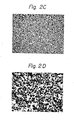
- the etched substrate 1 had a relatively uniformly and finely roughened back surface 6 as illustrated in FIG. 1D and FIG. 2C.
- the substrate 1 was washed with deionized water by ultrasonic cleaning for approximately two minutes, immersed in an aqueous hydrofluoric acid solution for approximately one minute and, then, immersed in a mixed solition of 30 parts by volume of nitric acid, one part by volume of hydrofluoric acid and 10 parts by volume of acetic acid.
- the so cleaned back surface had an appearance as shown in FIG. 2D.
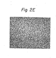
- the surface roughness thereof was approximately the same as that of the back surface mechanically sanded in a conventional manner by using an abrasive material having a particle size of 1,200 mesh.
- the silicon substrate 1 was then separated from the support 3 and, thereafter, washed with trichloroethylene to remove the wax from the substrate 1. Thereafter, a metal layer 7 was built up on the rough back surface of the substrate 1 to form an electrode connected to the collector region (FIG. lE).
- the formation of the collector electrode 7 may be effected by conventional means, such as electron beam evaporation, sputtering and plating.
- the collector electrode 7 may also be a two layer structure comprised of, for example, an underlying titanium layer and an upper nickel layer, or an underlying chromium layer and an upper silver layer.
- the metal layer structure may be suitably varied so as to obtain ohmic contact, and further, in consideration of the brazing material used for bonding the power transitor element to a stem.
- the transistor elements formed in the silicon substrate 1 were tested for their electrical properties. Thereafter, the silicon substrate 1 was subjected to dicing to be thereby divided into the discrete transistor elements (chips) 8.
- Each of the transistor elements 8 which satisfied the acceptance criteria was mounted on a metal stem 9 by using a solder 10, so that the metal layer formed on the roughened back surface faces the stem 9 (FIG. 1F).
- Terminal leads 11 were connected to the emitter electrode (not shown) and the base electrode (not shown) by aluminum wrirings 12 (FIG. 1F). Thereafter, a metal cap (not shown) was bonded to the stem 9 so that the transistor element 8 was airtightly sealed.
- the above-mentioned method of manufacturing a power transistor, wherein the silicon substrate is chemically etched is advantageous over the conventional method, wherein the silicon substrate is mechanically sanded, for the following reasons.
- the abrasive material used remains on the substrate and, further, a strained thin surface layer is undesirably formed on the substrate.
- the chemical etching of the invention does not have these defects.
- the mechanical sanding is liable to damage the substrate.
- the chemical etching of the invention i.e., the sequential steps illustrated in FIG. 1A through FIG.
- the power transistor manufactured by the method of the invention is similar to that manufactured by the conventional mechanical sanding procedure in the forward characteristics, such as the collector-emitter saturated voltage V CE (sat), and also, in the bond strength between the collector electrode and the silicon substrate.
- a silicon substrate having transistor elements formed therein was etched to a thickness of approximately 120 microns in a manner similar to that in EXAMPLE 1 (FIG. lB).
- the substrate after being adherend to the support 3, was subsjected to etching (no pre-etching was conducted) by immersing it in a etching solution having the same composition as that in Example 1, whereby the back surface thereof was roughened.
- the etched substrated was washed with deionized water by ultrasonic cleaning, immersed in an aqueous hydrofluoric acid solution and then, immersed in a mixed solution similar to that used in EXAMPLE 1, whereby a silicon substrate having a uniformly and finely roughened back surface was obtained.
- High frequency power transistors were made from the silicon substrate by conventional means.
- the thickness of a silicon substrate is usually reduced to 100 to 150 microns, in order to reduce the thermal resistance of the transistors.
- a silicon substrate cannot be sanded to such a thin thickness by the conventional sanding procedure without damaging the substrate.
- the chemical etching of the invention enables reduction of the thickness of the substrate to 100 to 150 microns without damage to the substrate.
- the silicon substrate as etched is washed with deionized water by ultrasonic cleaning and, then, immersed in an aqueous hydrofluoric acid solution in a manner similar to that mentioned in EXAMPLE 1 or 2, and the step of immersing the substrate in the mixed HN0 3/ HF/CH 3 COOH solution, mentioned in EXAMPLES 1 and 2, may be omitted. This is because there is no need of forming electrical contacts between the elements and the package.
- the method of the invention may be. ued in the manufacture of semiconductor substrates.
- the semiconductor substrate may be etched by using the etchant in a manner similar to that mentioned in the above examples. It is also possible to prepare a semiconductor substrate having the two predominant rough surfaces. In this case, the etching of the substrate is carried out without adherence of the substrate to a support.
Landscapes
- Weting (AREA)
Applications Claiming Priority (2)
| Application Number | Priority Date | Filing Date | Title |
|---|---|---|---|
| JP61228/79 | 1979-05-18 | ||
| JP6122879A JPS55153338A (en) | 1979-05-18 | 1979-05-18 | Surface treatment of semiconductor substrate |
Publications (2)
| Publication Number | Publication Date |
|---|---|
| EP0019468A1 true EP0019468A1 (fr) | 1980-11-26 |
| EP0019468B1 EP0019468B1 (fr) | 1984-08-08 |
Family
ID=13165140
Family Applications (1)
| Application Number | Title | Priority Date | Filing Date |
|---|---|---|---|
| EP80301595A Expired EP0019468B1 (fr) | 1979-05-18 | 1980-05-16 | Procédé de traitement superficiel d'un substrat semiconducteur |
Country Status (4)
| Country | Link |
|---|---|
| US (1) | US4294651A (fr) |
| EP (1) | EP0019468B1 (fr) |
| JP (1) | JPS55153338A (fr) |
| DE (1) | DE3068862D1 (fr) |
Cited By (3)
| Publication number | Priority date | Publication date | Assignee | Title |
|---|---|---|---|---|
| US5504022A (en) * | 1993-01-07 | 1996-04-02 | Fujitsu Limited | Method of making a semiconductor memory device having a floating gate |
| DE19806406C1 (de) * | 1998-02-17 | 1999-07-29 | Sez Semiconduct Equip Zubehoer | Verfahren zum Rauhätzen einer Halbleiter-Oberfläche |
| WO2005036629A1 (fr) * | 2003-10-10 | 2005-04-21 | Mimasu Semiconductor Industry Co., Ltd. | Procede de rugosification de la surface d'une plaquette |
Families Citing this family (19)
| Publication number | Priority date | Publication date | Assignee | Title |
|---|---|---|---|---|
| US4601784A (en) * | 1985-05-31 | 1986-07-22 | Morton Thiokol, Inc. | Sodium permanganate etch baths containing a co-ion for permanganate and their use in desmearing and/or etching printed circuit boards |
| US4601783A (en) * | 1985-05-31 | 1986-07-22 | Morton Thiokol, Inc. | High concentration sodium permanganate etch batch and its use in desmearing and/or etching printed circuit boards |
| JP2578798B2 (ja) * | 1987-04-23 | 1997-02-05 | 松下電器産業株式会社 | 半導体レ−ザ装置 |
| US4940510A (en) * | 1987-06-01 | 1990-07-10 | Digital Equipment Corporation | Method of etching in the presence of positive photoresist |
| US5223081A (en) * | 1991-07-03 | 1993-06-29 | Doan Trung T | Method for roughening a silicon or polysilicon surface for a semiconductor substrate |
| US5827784A (en) * | 1995-12-14 | 1998-10-27 | Texas Instruments Incorporated | Method for improving contact openings during the manufacture of an integrated circuit |
| JPH09260342A (ja) * | 1996-03-18 | 1997-10-03 | Mitsubishi Electric Corp | 半導体装置の製造方法及び製造装置 |
| US6248664B1 (en) * | 1997-05-19 | 2001-06-19 | Semiconductor Components Industries Llc | Method of forming a contact |
| US6600557B1 (en) * | 1999-05-21 | 2003-07-29 | Memc Electronic Materials, Inc. | Method for the detection of processing-induced defects in a silicon wafer |
| WO2000072368A1 (fr) * | 1999-05-21 | 2000-11-30 | Memc Electronic Materials, Inc. | Procédé d'attaque chimique d'une plaquette de silicium |
| US6482749B1 (en) | 2000-08-10 | 2002-11-19 | Seh America, Inc. | Method for etching a wafer edge using a potassium-based chemical oxidizer in the presence of hydrofluoric acid |
| US7067015B2 (en) * | 2002-10-31 | 2006-06-27 | Texas Instruments Incorporated | Modified clean chemistry and megasonic nozzle for removing backside CMP slurries |
| SG129274A1 (en) * | 2003-02-19 | 2007-02-26 | Mitsubishi Gas Chemical Co | Cleaaning solution and cleaning process using the solution |
| CN100546006C (zh) * | 2003-09-09 | 2009-09-30 | Csg索拉尔有限公司 | 蚀刻硅的改进方法 |
| JP2006191021A (ja) * | 2004-12-30 | 2006-07-20 | Siltron Inc | シリコンウェハのd−欠陥評価用腐蝕液、及びこれを利用した評価方法 |
| TWI275149B (en) * | 2005-05-09 | 2007-03-01 | Phoenix Prec Technology Corp | Surface roughing method for embedded semiconductor chip structure |
| EP2090675B1 (fr) * | 2008-01-31 | 2015-05-20 | Imec | Gravure de défauts de germanium |
| CN103187239B (zh) * | 2011-12-29 | 2015-11-25 | 无锡华润上华半导体有限公司 | 去除芯片上锡球的方法 |
| CN106252221A (zh) * | 2015-06-13 | 2016-12-21 | 中芯国际集成电路制造(上海)有限公司 | 刻蚀方法 |
Citations (2)
| Publication number | Priority date | Publication date | Assignee | Title |
|---|---|---|---|---|
| US2847287A (en) * | 1956-07-20 | 1958-08-12 | Bell Telephone Labor Inc | Etching processes and solutions |
| FR2374396A1 (fr) * | 1976-12-17 | 1978-07-13 | Ibm | Composition de decapage du silicium |
Family Cites Families (13)
| Publication number | Priority date | Publication date | Assignee | Title |
|---|---|---|---|---|
| US3309760A (en) * | 1964-11-03 | 1967-03-21 | Bendix Corp | Attaching leads to semiconductors |
| US3791948A (en) * | 1971-11-01 | 1974-02-12 | Bell Telephone Labor Inc | Preferential etching in g a p |
| US3833435A (en) * | 1972-09-25 | 1974-09-03 | Bell Telephone Labor Inc | Dielectric optical waveguides and technique for fabricating same |
| GB1447866A (en) * | 1972-11-10 | 1976-09-02 | Nat Res Dev | Charge coupled devices and methods of fabricating them |
| US3936331A (en) * | 1974-04-01 | 1976-02-03 | Fairchild Camera And Instrument Corporation | Process for forming sloped topography contact areas between polycrystalline silicon and single-crystal silicon |
| US3986251A (en) * | 1974-10-03 | 1976-10-19 | Motorola, Inc. | Germanium doped light emitting diode bonding process |
| NL7505134A (nl) * | 1975-05-01 | 1976-11-03 | Philips Nv | Werkwijze voor het vervaardigen van een half- geleiderinrichting. |
| US4137123A (en) * | 1975-12-31 | 1979-01-30 | Motorola, Inc. | Texture etching of silicon: method |
| DE2600990A1 (de) * | 1976-01-13 | 1977-07-21 | Wacker Chemitronic | Verfahren zum polieren von halbleiteroberflaechen, insbesondere galliumphosphidoberflaechen |
| DE2638302A1 (de) * | 1976-08-25 | 1978-03-02 | Wacker Chemitronic | Aetzmittel fuer iii/v-halbleiter |
| JPS5346633A (en) * | 1976-10-12 | 1978-04-26 | Nippon Electric Ind | Transistor inverter |
| US4171242A (en) * | 1976-12-17 | 1979-10-16 | International Business Machines Corporation | Neutral pH silicon etchant for etching silicon in the presence of phosphosilicate glass |
| US4147564A (en) * | 1977-11-18 | 1979-04-03 | Sri International | Method of controlled surface texturization of crystalline semiconductor material |
-
1979
- 1979-05-18 JP JP6122879A patent/JPS55153338A/ja active Granted
-
1980
- 1980-05-16 US US06/150,686 patent/US4294651A/en not_active Expired - Lifetime
- 1980-05-16 EP EP80301595A patent/EP0019468B1/fr not_active Expired
- 1980-05-16 DE DE8080301595T patent/DE3068862D1/de not_active Expired
Patent Citations (2)
| Publication number | Priority date | Publication date | Assignee | Title |
|---|---|---|---|---|
| US2847287A (en) * | 1956-07-20 | 1958-08-12 | Bell Telephone Labor Inc | Etching processes and solutions |
| FR2374396A1 (fr) * | 1976-12-17 | 1978-07-13 | Ibm | Composition de decapage du silicium |
Non-Patent Citations (1)
| Title |
|---|
| PATENT ABSTRACTS OF JAPAN, Vol. 3, Nr. 56, May 15, 1979 Tokyo (JP) & JP-A-54 034768 (HITACHI) * The whole document * * |
Cited By (4)
| Publication number | Priority date | Publication date | Assignee | Title |
|---|---|---|---|---|
| US5504022A (en) * | 1993-01-07 | 1996-04-02 | Fujitsu Limited | Method of making a semiconductor memory device having a floating gate |
| DE19806406C1 (de) * | 1998-02-17 | 1999-07-29 | Sez Semiconduct Equip Zubehoer | Verfahren zum Rauhätzen einer Halbleiter-Oberfläche |
| EP0938133A3 (fr) * | 1998-02-17 | 1999-11-03 | SEZ Semiconductor-Equipment Zubehör für die Halbleiterfertigung AG | Procédé d'attaque pour former une surface de semiconducteur rugueuse |
| WO2005036629A1 (fr) * | 2003-10-10 | 2005-04-21 | Mimasu Semiconductor Industry Co., Ltd. | Procede de rugosification de la surface d'une plaquette |
Also Published As
| Publication number | Publication date |
|---|---|
| JPH0121618B2 (fr) | 1989-04-21 |
| DE3068862D1 (en) | 1984-09-13 |
| JPS55153338A (en) | 1980-11-29 |
| EP0019468B1 (fr) | 1984-08-08 |
| US4294651A (en) | 1981-10-13 |
Similar Documents
| Publication | Publication Date | Title |
|---|---|---|
| US4294651A (en) | Method of surface-treating semiconductor substrate | |
| Sullivan et al. | Electroless nickel plating for making ohmic contacts to silicon | |
| US3597658A (en) | High current semiconductor device employing a zinc-coated aluminum substrate | |
| US5298459A (en) | Method of manufacturing semiconductor device terminal having a gold bump electrode | |
| US4125648A (en) | Electroless deposition of nickel on aluminum | |
| US5344524A (en) | SOI substrate fabrication | |
| US5695557A (en) | Process for producing a semiconductor substrate | |
| US3480412A (en) | Method of fabrication of solder reflow interconnections for face down bonding of semiconductor devices | |
| JP4811756B2 (ja) | 金属−セラミックス接合回路基板の製造方法 | |
| US3241931A (en) | Semiconductor devices | |
| US2995475A (en) | Fabrication of semiconductor devices | |
| GB1053069A (fr) | ||
| US2906647A (en) | Method of treating semiconductor devices | |
| US3747202A (en) | Method of making beam leads on substrates | |
| US2916806A (en) | Plating method | |
| US3489603A (en) | Surface pretreatment process | |
| US3791861A (en) | Method for producing thin film circuits on high purity alumina substrates | |
| US3947304A (en) | Etching of group III-V semiconductors | |
| US3483610A (en) | Thermocompression bonding of foil leads | |
| JPH07235651A (ja) | 半導体基板およびその作製方法 | |
| EP0349065B1 (fr) | Procédé d'assemblage de deux corps | |
| US6248664B1 (en) | Method of forming a contact | |
| US2935781A (en) | Manufacture of germanium translators | |
| CN109103080A (zh) | 一种带电极的反向台面超薄晶片及其制备方法 | |
| US3661727A (en) | Method of manufacturing semiconductor devices |
Legal Events
| Date | Code | Title | Description |
|---|---|---|---|
| PUAI | Public reference made under article 153(3) epc to a published international application that has entered the european phase |
Free format text: ORIGINAL CODE: 0009012 |
|
| 17P | Request for examination filed | ||
| AK | Designated contracting states |
Designated state(s): DE FR GB NL |
|
| GRAA | (expected) grant |
Free format text: ORIGINAL CODE: 0009210 |
|
| AK | Designated contracting states |
Designated state(s): DE FR GB NL |
|
| REF | Corresponds to: |
Ref document number: 3068862 Country of ref document: DE Date of ref document: 19840913 |
|
| ET | Fr: translation filed | ||
| PLBE | No opposition filed within time limit |
Free format text: ORIGINAL CODE: 0009261 |
|
| STAA | Information on the status of an ep patent application or granted ep patent |
Free format text: STATUS: NO OPPOSITION FILED WITHIN TIME LIMIT |
|
| 26N | No opposition filed | ||
| PGFP | Annual fee paid to national office [announced via postgrant information from national office to epo] |
Ref country code: GB Payment date: 19900508 Year of fee payment: 11 |
|
| PGFP | Annual fee paid to national office [announced via postgrant information from national office to epo] |
Ref country code: NL Payment date: 19900531 Year of fee payment: 11 Ref country code: FR Payment date: 19900531 Year of fee payment: 11 |
|
| PGFP | Annual fee paid to national office [announced via postgrant information from national office to epo] |
Ref country code: DE Payment date: 19900723 Year of fee payment: 11 |
|
| PG25 | Lapsed in a contracting state [announced via postgrant information from national office to epo] |
Ref country code: GB Effective date: 19910516 |
|
| PG25 | Lapsed in a contracting state [announced via postgrant information from national office to epo] |
Ref country code: NL Effective date: 19911201 |
|
| GBPC | Gb: european patent ceased through non-payment of renewal fee | ||
| NLV4 | Nl: lapsed or anulled due to non-payment of the annual fee | ||
| PG25 | Lapsed in a contracting state [announced via postgrant information from national office to epo] |
Ref country code: FR Effective date: 19920131 |
|
| PG25 | Lapsed in a contracting state [announced via postgrant information from national office to epo] |
Ref country code: DE Effective date: 19920303 |
|
| REG | Reference to a national code |
Ref country code: FR Ref legal event code: ST |